

Abstract
The family of MAX phase compounds has emerged as promising engineering materials with potential applications in various fields, including supercapacitors. Radio frequency sputtering, a low-temperature thin-film deposition process, allows for the precise deposition of Ti-Al-C multilayers. This study investigates the key steps in the formation of Ti3AlC2 thin films on a copper substrate by converting Ti-Al-C multilayers as a function of annealing conditions. X-ray diffraction, scanning electron microscopy analysis, UV-visible spectroscopy, and FTIR spectroscopy provide structural insights. These findings provide significant insights into the development of binder-free and environmentally friendly anodes with copper current collectors. The versatility and performance of our approach make it a promising candidate for the growing demand in the supercapacitor and battery industries.
Keywords: Ti3AlC2 MAX phase, Carbides, Structural investigation, Heat treatment, Gas atmosphere, RF sputtering, Supercapacitor
Subject terms: Chemistry, Energy science and technology, Materials science, Nanoscience and technology, Physics
Introduction
The MAX phase compounds have recently emerged as a novel class of engineering materials with significant potential for applications in various fields, including batteries and supercapacitors1,2. These materials are defined by the general formula Mn+1AXnMn+1AXn (where n can be 1, 2, or 3, corresponding to the 211, 312, or 413 phases, respectively)3–5. Comprising carbides and binary nitrides of transition metals, MAX phases exhibit numerous advantageous properties, such as low density, a low thermal expansion coefficient, high elastic stiffness, and high melting points6,7. Moreover, they display metallic-like characteristics, including machinability, high electrical and thermal conductivity, considerable ductility, high thermal shock resistance, exceptional damage tolerance, excellent mechanical properties at elevated temperatures, and in some cases, even oxidation resistance6,7.
It is noteworthy that a prominent group of two-dimensional materials, known as MXenes, is derived from MAX phases through selective etching of the “A” layer8–10. MAX phases themselves can be synthesized via various methods, which are broadly categorized as top-down or bottom-up. The top-down approach typically involves the incorporation of elements into the “A” layer, while bottom-up methods, such as powder synthesis or thin-film deposition, enable direct fabrication11–16.
A common technique for synthesizing MAX phases is hot isostatic pressing (HIP), which utilizes elemental and/or binary stoichiometric ceramic powders. This method requires high temperatures and pressures, combined with prolonged reaction times, to ensure the complete conversion of precursors into the MAX phase17.
Conventional electrode synthesis for supercapacitors and lithium-ion batteries often involves numerous chemicals, leading to high costs, environmental concerns, and prolonged processing times. Thin-film fabrication technologies, such as chemical vapor deposition (CVD) or physical vapor deposition (PVD), enable the direct production of electrodes (anodes or cathodes) without additional steps like the use of adhesives, thereby mitigating these issues. Moreover, magnetron sputtering, in particular, offers distinct advantages through the deposition of dense, high-purity thin films with controlled crystalline structure (single-crystalline or polycrystalline)18,19.
Table 1 summarizes recent studies on the synthesis of MAX phase thin films on various substrates. Copper foil is widely employed as a current collector, particularly in lithium-ion batteries, owing to its excellent electrical conductivity, favorable mechanical properties, and strong chemical compatibility. Although copper offers these advantages, the formation and properties of MAX phase thin films on copper substrates remain largely unexplored. It should be noted that metallic copper is highly reactive and can readily diffuse into adjacent material structures20. However, for applications requiring p-type semiconductors, the presence of copper compounds may indeed be beneficial.
Table 1.
Recent studies on the synthesis of MAX phase thin films via sputtering techniques.
| Coating | Substrate | Annealing Temp. | Annealing Atm. | Ref. | |
|---|---|---|---|---|---|
| 1 | V2AlC-AlOx heterostructures | MgO (001) | 580 °C | Ar gas | 21 |
| 2 | Ti2AlC | - | 800 °C & 1000 °C | Vacuum | 22 |
| 3 | Ti2AlC | TiAl48-2-2 | 800 °C | - | 23 |
| 4 | (TiVCr)2AlC | c-plane sapphire & quartz | 700–900 °C | Vacuum | 24 |
| 5 | Cr2AlC, Ti3AlC2 or Ti2AlC | TiAl alloys | 500 & 1000 °C | - | 25 |
| 6 | Ti2AlC | Al2O3 | 900 °C | Vacuum | 26 |
| 7 | Amorphous Cr-Al-C |
Polycrystalline YSZ |
- | Ar gas | 27 |
| 8 | Ti2AlC | Zirlo alloy | 550 °C | Ar gas | 28 |
| 9 | Ti-Al-C film | Steel | 200–800 °C | - | 29 |
| 10 | Ti2AlC | Si & SiO2/Si | 600 °C & 700 °C | Ar gas | 17 |
The use of a copper substrate imposes a significant constraint on the maximum achievable annealing temperature due to its relatively low melting point (1085 °C) and the tendency to form brittle intermetallic phases and undergo excessive grain growth at elevated temperatures, which can compromise mechanical integrity. This limitation potentially prevented the attainment of higher phase purity and crystallinity in the synthesized MAX films, which typically require high-temperature treatments.
The present work focuses on the synthesis of Ti-Al-C multilayer thin films via the direct deposition of elemental layers (Ti, Al, C) onto a copper substrate using radio frequency (RF) sputtering, followed by post-deposition annealing. This study investigates the influence of annealing conditions, temperature and atmosphere, on the surface morphology and microstructure of the resulting films. A particular emphasis is placed on the role of an argon atmosphere during annealing, which is crucial when using a copper substrate due to its high reactivity. The presence of argon mitigates unwanted oxidation and facilitates controlled phase formation30.
To conclude, a quasi-solid-state supercapacitor cell was assembled to evaluate the electrochemical performance. The device incorporated a binder-free graphite/reduced graphene oxide (rGO) cathode31 paired with a binder-free anode from the investigated samples.
Experimental work
Thin film deposition
The sputtering process involved the sequential deposition of thin layers of titanium (M), aluminum (A), and carbon (X) onto a copper foil substrate using high-purity (≈ 98%) titanium, aluminum, and graphite targets. The deposition was conducted in an argon atmosphere (≈ 98% purity) at a constant pressure, with the layer thicknesses carefully controlled to closely resemble the stoichiometry of the target MAX phase, as detailed in Table 2. The substrate was a 30 μm-thick copper foil with an electrical resistance of 1.678 µΩ/cm at 20 °C.
Table 2.
Sputtering parameters used for the deposition of the Ti-Al-C multilayer structure on the copper substrate.
| Target element | RF power (W) | Deposition time (Sec) | Gas flow (SCCM) |
|---|---|---|---|
| Ti | 90 | ⁓400 | 30 |
| Al | 90 | ⁓600 | 30 |
| C | 90 | ⁓400 | 30 |
The deposition was performed over two consecutive cycles (Fig. 1). The chamber’s base pressure was maintained at approximately 1 × 10⁻⁷ Torr using a mechanical pump in conjunction with a turbomolecular pump. Before deposition, the substrates were ultrasonically cleaned in acetone and isopropyl alcohol for 10 min in each solvent.
Fig. 1.

The schematic of (a) the sputtering deposition method, (b) a multilayer structure on Cu foil substrate, (c) deposited multilayer structure, (d) Thermal annealing in Argon atmosphere, and (e) the resulting sample with the 2D schematic of Max phase.
Annealing processes
To achieve the MAX phase formation (as confirmed by the results in Table 3), the samples were placed in a quartz boat and annealed under two different atmospheric conditions. The first set was annealed in air at 500 °C and 600 °C for one hour. Alternatively, a second set was annealed under a flowing argon atmosphere (≈ 98% purity) at the same temperatures and duration. Following annealing, all samples were allowed to cool fully to room temperature prior to subsequent analysis.
Table 3.
Annealing conditions for Ti–Al–C multilayers on copper substrate.
| Sample | Temperature (˚C) | Duration (h) | Atmosphere |
|---|---|---|---|
| S-1 | 500 | 1 | Air |
| S-2 | 600 | 1 | Air |
| S-3 | 500 | 1 | Ar gas (≈ 98%), 13 sccm |
| S-4 | 600 | 1 | Ar gas (≈ 98%), 13 Sccm |
Physical characterization
The crystalline phases of the samples were characterized by X-ray diffraction (XRD) using a diffractometer (Rigaku, Japan) with Cu Kα radiation (λ = 1.5406 Å). Measurements were performed over a 2θ range of 20° to 60° with a step size of 0.02°.
The surface morphology and microstructure of the samples were examined using field-emission scanning electron microscopy (FESEM, TESCAN-MIRA3) at an acceleration voltage of 5 kV. This technique provided high-resolution images for detailed microstructural analysis.
Elemental analysis was conducted using energy-dispersive X-ray spectroscopy (EDS), including elemental mapping, to determine the chemical composition and spatial distribution of elements within the samples.
Optical absorption properties were characterized by UV-Vis spectroscopy (PhysTec, MA-2500).
Fourier-transform infrared (FTIR) spectroscopy was performed using a BRUKER TENSOR 27 spectrometer (Germany) to investigate the structural and bonding characteristics of the samples. Transmission spectra were acquired at room temperature over a wavenumber range of 4000 to 650 cm⁻¹ with a resolution of 4 cm⁻¹.
The combination of characterization techniques—XRD, FESEM, EDS, and FTIR—provided a comprehensive analysis of the samples’ crystalline structure, surface morphology, elemental composition, and chemical bonding. This multi-faceted approach enabled a thorough understanding of the materials’ properties and the effects of processing parameters.
Chemical characterization
A quasi-solid-state high-voltage supercapacitor (SC) cell was assembled using binder-free electrodes to evaluate its electrochemical performance. The cell consisted of a graphite/reduced graphene oxide (rGO) composite cathode and the S-4 sample as the anode.
Cathode preparation
A 0.8 mm-thick graphite sheet was cut into 1 × 2 cm² pieces to serve as the current collector. Then, 200 µL of an rGO precursor solution was drop-cast onto a 1 × 1 cm² area of the graphite substrate. The coated electrode was dried at temperatures below 100 °C.
Electrolyte and cell assembly
The gel electrolyte was prepared by gradually adding 5 mL of a 1.7 M NaCl aqueous solution to a 0.0025 M polyvinylpyrrolidone (PVP) solution under stirring. A 1 × 1 cm² solid-state cell was constructed by placing a separator (Whatman, Grade GF/C) between the cathode and anode. The assembly was securely sealed using adhesive tape to ensure mechanical stability during testing.
Cyclic voltammetry (CV) was performed over a voltage range of -1 to 1 V at different scan rates. Simultaneously, galvanostatic charge/discharge (GCD) tests were conducted within the voltage range of 0 to 1 V at various current densities. These experiments were executed utilizing an Origa Master 5 potentiostat.
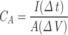
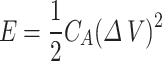
The electrochemical properties of the areal capacitance (CA), the areal energy density (E), and the areal power density (p) were calculated from a galvanostatic charge/discharge (GCD) curve according to the following Eq.
 |
1 |
 |
2 |
 |
3 |
Where I is the Current density in amperes, A is the active area of the electrode in cm2, ∆V is the potential drop in volts, and ∆t is the discharging time in seconds of the GCD curve31.
Result and discussion
Figure 2 presents FESEM images of the Ti–Al–C multilayer thin film deposited on the copper substrate under the conditions detailed in Table 2. The film consists of densely packed, uniformly distributed nanoparticles with an average size ranging from 60 to 80 nm. These nanoparticles exhibit a spherical morphology and homogeneous coverage across the substrate surface. The multilayer has a measured thickness of approximately 12 μm.
Fig. 2.

FESEM (a) top-view, and (b) cross-section images of a (Ti-Al-C) multilayer on a Cu substrate following the conditions outlined in Table 2.
Energy-dispersive X-ray spectroscopy (EDS) is a fundamental and widely employed technique for material characterization. This method involves irradiating a sample with a high-energy electron beam, inducing the emission of characteristic X-rays with energies specific to each element. EDS enables rapid, non-destructive, and accurate determination of elemental composition. To assess the spatial homogeneity and distribution of elements within the Ti–Al–C multilayer thin films on the copper substrate, elemental mapping was conducted (Fig. 3).
Fig. 3.

(a) Elemental maps of Ti, Al, and C, (b) EDS results of the Ti-Al-C multilayer deposited on a Cu substrate according to the specifications outlined in Table 2.
As shown in Fig. 3a, the multilayer exhibits a uniform morphological structure. Elemental composition analysis via EDS (Fig. 3b) revealed a titanium-to-carbon (Ti/C) atomic ratio of 0.05 and a titanium-to-aluminum (Ti/Al) ratio of 2.08. The Ti/Al ratio closely approximates the ideal stoichiometric value of 3:1 (i.e., Ti₃AlC₂), indicating successful formation of the target MAX phase. However, the carbon content was found to be significantly higher than expected. This deviation may be attributed to the inherent limitations of EDS in accurately quantifying light elements, such as carbon, due to their low X-ray yield and absorption effects.
Ultraviolet-visible (UV-Vis) spectroscopy was performed to investigate the optical properties of the as-deposited multilayer and annealed samples (Fig. 4). The as-deposited multilayer and all annealed samples exhibited low absorbance (less than 2%), with an absorption edge observed around 545 nm (Fig. 4a). However, annealing resulted in a noticeable increase in absorbance, particularly within the visible region. The use of an argon atmosphere during annealing led to significantly enhanced light absorption in samples S-3 and S-4. Notably, sample S-4, annealed at 600 °C under argon, demonstrated the highest absorption among all samples.
Fig. 4.

(a) The UV-Vis absorbance spectroscopy of multilayer thin film (Ti-Al-C) deposited on Cu substrates and samples annealed according to Table 3, (b) The indirect band gap energy of S-1, using Tauc’s relation.
The optical bandgap energy was determined using Tauc’s method, by extrapolating the linear region of the (αhν)ⁿ versus photon energy (hν) plot, where n = 0.5 for indirect and n = 2 for direct bandgap transitions. An example of the Tauc plot for indirect bandgap estimation is presented in Fig. 4b. The calculated bandgap values (summarized in Table 4) indicate that all samples possess wide band gaps. Wide bandgap materials are known to exhibit high intrinsic breakdown strength32, which is advantageous for electrode applications as it reduces the probability of mechanical failure (e.g., cracking) during operation. However, a trade-off of wide band gaps is typically lower electrical conductivity.
Table 4.
The direct and indirect band gap energy of the samples (Table 3) using the UV-Vis spectroscopy and the Tauc’s relation.
| Sample | S-1 | S-2 | S-3 | S-4 |
|---|---|---|---|---|
| Direct band gap (eV) | 3.4 | 3.7 | 3.0 | 2.7 |
| Indirect band gap (eV) | 3.4 | 3.8 | 3.0 | 1.7 |
Virtually all electrochemical processes involve the simultaneous transfer of electrons and ions at the electrode–electrolyte interface. As a result, high electrical conductivity is crucial to facilitate efficient charge transport, improve rate capability, enhance reaction kinetics, and maximize the utilization of active materials. For example, in battery systems, a small band gap promotes rapid electron transfer, leading to high power density and exceptional rate performance.
Therefore, improving the electrical conductivity of wide-bandgap materials is vital for enhancing their performance in practical applications. Several strategies can be employed to achieve this, including chemical doping, optimization of crystalline quality and defect control, and the construction of heterostructures33.
In general, the S-4 sample exhibits both direct and indirect band gaps, measuring 2.7 eV and 1.7 eV, respectively. These values are lower than those of the other samples, suggesting superior electrical conductivity.
X-ray diffraction (XRD) analysis was performed over a 2θ range of 10° to 70° to evaluate the phase composition of the annealed films under different conditions (as detailed in Table 3). The hexagonal crystal structure of MAX phases is defined by two primary lattice parameters: the in-plane parameter a, which governs the basal plane dimensions, and the out-of-plane parameter c, which corresponds to the unit cell height. The lattice parameter a can be determined from the (110) diffraction peak, typically located near 59°, while the parameter c is derived from the (002) peak, which appears between 5° and 15° depending on the specific MAX phase composition34. It is noteworthy that a shift in diffraction peaks toward lower angles indicates an expansion in the interlayer spacing, whereas a shift toward higher angles corresponds to a contraction in the interplanar distance35. (Fig. 5).
Fig. 5.

XRD patterns of (Ti-Al-C) multilayer deposited on a Cu substrate, and annealing for one hour according to the specifications outlined in Table 2: (S-1) at 500 °C in an air atmosphere, (S-2) at 600 °C in an air atmosphere, (S-3) at 500 °C in the presence of argon gas and (S-4) at 600 °C in the presence of argon gas.
Figure 5 displays the XRD profiles of the annealed multilayer samples under various conditions. The samples contain copper compounds originating from the substrate, along with the Ti3AlC2 MAX phase and the TiC MXene. The diffraction peaks in the patterns reveal the characteristic reflections of the Ti3AlC2 phase (JCPDS, No.52–0875), located at approximately 34, 36, 39, 42, 49, and 60 degrees, corresponding to the (101), (103), (104), (105), (107), and (110) crystal planes, respectively. It should be noted that the primary peak associated with the stratified arrangement of Ti3AlC2 at 2θ = 9.6˚ has not been pinpointed in any of the samples.
One of the remarkable observations is the effect of the substrate material. Copper is very reactive and can easily penetrate the film structure. The presence of argon gas during annealing at high temperatures (samples S-3 and S-4) has led to a decrease in the peak of about 43˚ related to copper compared to other samples. It is noteworthy to highlight that CuO and Cu2O are both P-type semiconductors and stable forms of copper oxides. CuO has a band gap of approximately 1.4 eV36, while Cu2O has a band gap of around 2.0 eV20. These two materials have significant applications in negative electrode materials37.
In sample S-1, peaks corresponding to Al2O3 at 2θ = 43.5˚ and 68.4˚ can be identified. Similarly, sample S-2 exhibits detectable peaks of Al2O3 at 2θ = 51.7˚ and 66.84˚. Nonetheless, the peaks associated with aluminum are absent in the S-3 and S-4 samples. Utilization of argon gas during annealing serves as a preventive measure against the formation of aluminum oxide. This is crucial due to aluminum’s strong tendency to oxidize. By employing argon gas, we can ensure that aluminum is fully integrated into the structure, facilitating the formation of the desired MAX phase.
Interestingly, the carbon peak at around 28° has disappeared in the S-4 sample. This can be attributed to the formation of the TiC MAX phase at around 36°, which corresponds to the (111) lattice plane. This formation of the TiC MAX phase occurs in the presence of argon gas at temperatures exceeding 500 °C. This phase formation can be elucidated by the accelerated alloying process that occurs at elevated temperatures and in the presence of argon gas. It is understood that the chemical bond found in the MAX and TiC phases exhibits a covalent characteristic of an ion-metal blend, resulting in a blend of ceramic and metallic traits.
It is important to mention that the use of extremely high temperatures was limited in this study due to the brittleness of the copper substrate.
It is observed that the distinct Ti3AlC2 (002) peak at approximately 9.6° is absent, which may be attributed to textural effects or insufficient phase purity. This phenomenon is likely due to the incorporation of copper oxide compounds into the MAX phase structure, resulting in the formation of a composite material. The formation of this composite can be explained by three possible mechanisms:
Substitution of certain copper or oxygen atoms onto aluminum sites within the crystal lattice,
Intercalation of copper oxide clusters or layers within the MAX phase structure, or
Surface deposition of a copper oxide layer onto the MAX phase.
Based on the observed homogeneous distribution of Cu and O in the EDS elemental maps, the substitution or intercalation mechanisms appear more plausible than surface deposition.
The crystallite size was determined using the Scherrer equation (D = Kλ/βcosθ), applied to the dominant XRD diffraction peaks observed at 2θ values of approximately 35°, 43°, and 50° (Fig. 6). The results demonstrate that the crystallite sizes in all samples are below 40 nm. Among the investigated samples, S-1 exhibited the smallest crystallites, with sizes ranging from 15 to 24 nm, indicating a notably finer microstructure.
Fig. 6.

The estimated crystallite size using the Scherrer equation, at 2θ approximately 35°, 43°, and 50° as a function of annealing conditions.
The FESEM images of the samples under different annealing conditions are presented in Fig. 7. Unique morphologies can be distinguished for each set of annealing parameters (Fig. 7a–d).
Fig. 7.


FESEM top-view images of (Ti-Al-C) multilayer deposited on a Cu substrate, and annealing for one hour according to the specifications outlined in Table 2: (S-1) at 500 °C in an air atmosphere, (S-2) at 600 °C in an air atmosphere, (S-3) at 500 °C in the presence of argon gas and (S-4) at 600 °C in the presence of argon gas.
When the samples were annealed without the presence of argon gas (Fig. 7a,b), nanorods were visible within the structure. The quantity and size of these nanorods diminished as the annealing temperature was increased.
In contrast, the morphology and growth of the particles exhibited significant differences when the layers were annealed in the presence of argon gas (Fig. 7c,d). The structures of samples S-3 and S-4 are composed of distinctly different arrangements of cylindrical and polyhedral shapes.
These polyhedra are stacked on top of each other, making it challenging to discern their individual boundaries. Interestingly, no nanorods were observed in the samples annealed under the argon gas atmosphere. Furthermore, increasing the annealing temperature from 500 °C to 600 °C transformed the particle shape from a cylindrical geometry (approximately 80 to 120 nm for the sample in Fig. 7c) to a porous polyhedral structure (Fig. 7d).
The notable change in morphology and growth behavior of the particles can be attributed to the influence of the annealing atmosphere. The presence of argon gas during the annealing process appears to have prevented the formation of the nanorods observed in the samples annealed without argon. Additionally, the higher annealing temperature of 600 °C promoted the transformation of the particles from a cylindrical to a more complex, porous polyhedral shape.
To enhance the comprehension of the structure following annealing at 600 °C in an argon atmosphere, FESEM cross-sectional images of sample S-4 are presented in Fig. 8. As shown in Fig. 8b, the layered porous nanostructure is clearly visible.
Fig. 8.

FESEM cross-section images of the S-4 sample.
EDS elemental analysis was performed on two components, namely Nanorod (component A) and the background (component B), to determine the composition of the nanorods as shown in Fig. 9. The analysis revealed that the nanorods primarily consist of aluminum, which were transformed into nanorods with the assistance of copper element (small fins in Fig. 7a). In accordance with the XRD analysis, which confirmed the presence of peaks corresponding to aluminum compounds (Fig. 5a,b). Consequently, annealing in the presence of argon gas led to a decrease in the amount of aluminum extracted from the structure, resulting in more favorable outcomes in achieving the MAX phase.
Fig. 9.

The EDS results of (Ti-Al-C) multilayer annealed for one hour at 500 °C in an air atmosphere.
Additionally, ATR-FTIR spectroscopy was employed to analyze the structure and composition, as well as the details of bonding. The spectra obtained from S-1 and S-2 (Fig. 10a) displayed distinct bands corresponding to the stretching vibrations of OH groups (approximately 3658 cm− 1), which are indicative of the annealing process in the air atmosphere. Conversely, these bands were absent when argon gas was used (Fig. 10b). Additionally, stretching vibrations of the C-H group were observed in all samples within the 3000 to 2800 cm− 1 range. The weaker peak around 1453 cm− 1 was attributed to the C-H bending vibration38. On the other hand, the peak in the range of 1700 cm− 1 was assigned to the C = O stretching vibration of the COOH group39. The absorption peak around 1371 and 1386 cm− 1 is related to the OH bending vibration. On the other hand, bands in the range of 1400 to 1000 cm− 1 related to C-O stretching vibrations are less observed in samples S-3 and S-4. Due to the application of argon gas during the annealing process, a larger amount of carbon has entered the structure. Also, the bands at about 900 cm− 1 are related to C = C-H bonds, which can be seen in two samples, S-1 and S-2 (Fig. 10a), which are caused by the carbon bonds formed in the structure. In the range of 750–900 cm− 1, there exist bands resulting from Al-O bond vibrations40. The observation of Al-O bond vibrations is evident in samples S-1 and S-2. The vibration of the Al-OH bond can be associated with the band within the range of 937–980 cm− 1, which was no longer present after annealing with argon gas (Fig. 10b).
Fig. 10.

The FTIR spectrum of (Ti-Al-C) multilayer deposited on a Cu substrate, and annealing for one hour according to the specifications outlined in Table 3: (S-1) at 500 °C in an air atmosphere, (S-2) at 600 °C in an air atmosphere, (S-3) at 500 °C in the presence of argon gas, and (S-4) at 600 °C in the presence of argon gas.
The electrochemical performance is directly dependent on the sample morphology. The interconnected, porous polyhedral network facilitates ion diffusion and provides a significantly larger electroactive surface area compared to the nanorod structure. Although the nanorod morphology offers a high specific surface area, its performance is likely limited by poorer electrical connectivity between individual rods and longer, more tortuous ion diffusion pathways. Furthermore, the porous polyhedral network effectively accommodates volume changes during cycling, reducing mechanical degradation and ensuring long-term structural integrity. A more detailed investigation of these mechanisms could be the subject of future studies.
Cyclic voltammetry (CV) was performed to assess the electrochemical performance of the S-4 sample (Fig. 11a) at scan rates ranging from 10 to 100 mV s⁻¹. The configuration of the supercapacitor (SC) utilizing S-4 as the anode is described in the experimental section. As shown in Fig. 11a, well-defined redox peaks are observed across all scan rates, indicative of a quasi-capacitive charge storage mechanism in the cell with the S-4 anode. It is noteworthy that these redox peaks show a minor shift with increasing scan rate, suggesting rapid kinetics for ion insertion and extraction. Moreover, it is essential to emphasize that the samples, particularly S-4, contain not only the MAX phase but also copper compounds, which significantly influence the electrode’s electrochemical characteristics41–43.
Fig. 11.

Electrochemical characterization of the fabricated SC sample. (a) CV curves with different scan rates, (b) GCD profiles recorded at 50 mVs− 1 at different current densities.
Further insights were obtained from galvanostatic charge-discharge (GCD) tests (Fig. 11b) conducted at current densities of ± 0.2, ± 0.5, and ± 1 mA cm⁻². The nearly symmetrical triangular shape of the GCD profiles is maintained even at elevated current densities. The consistent charge and discharge durations reflect the excellent reversibility and high Coulombic efficiency of the assembled device.
The areal capacitance (CA), energy density (E), and power density (P) were calculated from the GCD data using Eq. (1) to (3). Both the areal capacitance and energy density show a significant decreasing trend with increasing current density (Table 5). This is because higher current densities do not provide sufficient time for complete charge transfer within the porous structure, limiting electrolyte ion access to the inner regions of the electrode and thus reducing the utilized capacitance44. However, it is important to note that the capacitance remains stable over successive cycles at each current density (Fig. 11b). The porous polyhedral morphology of S-4 appears to mitigate polarization at higher current densities during both charging and discharging, resulting in superior power density.
Table 5.
The areal capacitance (CA), energy density (E), and power density (p) at various current densities.
| Current density (mA cm− 2) | CA (mFcm− 2) | E (mWh cm− 2) | P (mWcm− 2) |
|---|---|---|---|
 0.2 0.2 |
8.60 | 4.30 | 361.30 |
 0.5 0.5 |
5.70 | 2.80 | 875.00 |
 1.0 1.0 |
1.90 | 1.90 | 1800.30 |
Conclusion
The objective of this study was to present a straightforward and cost-effective method for producing binder-free negative electrodes using the Ti₃AlC₂ MAX phase directly on a copper current collector. We successfully demonstrated that the microstructure of the synthesized MAX phase is highly tunable by controlling the annealing temperature and atmosphere, enabling the formation of specific morphologies—from cylindrical tubes to porous polyhedrons—tailored for electrochemical applications.
Looking forward, this in-situ synthesis approach offers distinct advantages for device integration compared to traditional powder-based methods. Conventional electrode manufacturing involves synthesizing MAX phase powder, mixing it with conductive additives and polymer binders, and then casting the slurry onto a current collector. Our method eliminates these complex, multi-step slurry processing stages, thereby streamlining fabrication and reducing costs. More importantly, the direct growth of the active material on the current collector ensures excellent electrical contact and mechanical adhesion, which are crucial for rate capability and long-term cycling stability in devices such as Li-ion batteries or supercapacitors.
From a scaling perspective, the techniques employed—magnetron sputtering and annealing—are already well-established and scalable industrial processes. Future work will focus on optimizing these processes for continuous roll-to-roll manufacturing, which would be a significant step towards the commercial realization of these binder-free electrodes. Furthermore, while the copper substrate was chosen for its conductivity, its reactivity was noted; investigating more inert or tailored substrates will be a key area of subsequent research to enhance electrochemical performance.
In summary, this work not only provides a straightforward pathway for creating alternative anodes but also outlines a versatile platform for the direct and integrable synthesis of MAX phase electrodes, offering a promising route for next-generation energy storage devices.
Expressing gratitude
We would like to express our sincere gratitude to the Institute for Research in Fundamental Physics (IPM) for their invaluable support in providing the necessary laboratory facilities and resources for this research project.
Access to state-of-the-art equipment, infrastructure, and the collaborative environment at these esteemed institutions has been instrumental in enabling the successful completion of this work.
Acknowledgements
We would like to express our sincere gratitude to the Institute for Research in Fundamental Physics (IPM) for their invaluable support in providing the necessary laboratory facilities and resources for this research project.The access to state-of-the-art equipment, infrastructure, and the collaborative environment at these esteemed institutions have been instrumental in enabling the successful completion of this work.
Author contributions
F.R. Data curation, Formal analysis, Conceptualization, original draft, Writing – review & editing, A.S. Methodology, Project administration, Writing – review & editing, Supervision, resources, Validation.
Data availability
All data generated or analyzed during this study are available from the corresponding author upon reasonable request.
Declarations
Competing interests
The authors declare no competing interests.
Ethics approval
The article has been written by the stated authors who are ALL aware of its content and approve its submission.
Consent to participate
The article has been written by the stated authors who are ALL aware of its content and approve its submission.
Consent for publication
If accepted, the article will not be published elsewhere in the same form, in any language, without the written consent of the publisher.
Footnotes
Publisher’s note
Springer Nature remains neutral with regard to jurisdictional claims in published maps and institutional affiliations.
References
- 1.Wang, L. et al. Intercalation of protons into sodium vanadium bronzes induced from the phase transition of V2CTx MXene for zinc ion batteries. J. Power Sources. 624, 235581. 10.1016/j.jpowsour.2024.235581 (2024). [Google Scholar]
- 2.J. H. R. Huang et al. Novel synthesis of B-doped Ti3C2Tx thin sheets via BF3 Lewis acid etching: structural insights and supercapacitor applications. J. Power Sources. 615, 235044. 10.1016/j.jpowsour.2024.235044 (2024). [Google Scholar]
- 3.Dahlqvist, M., Barsoum, M. W. & Rosen, J. MAX phases–Past, present, and future. Mater. Today. 72, 1–24. 10.1016/j.mattod.2023.11.010 (2024). [Google Scholar]
- 4.Y. & Pan W2AlC: A new layered MAX phase to adjust the balance between strength and ductility. Mater. Today Chem.35, 101915. 10.1016/j.mtchem.2024.101915 (2024). [Google Scholar]
- 5.I. Ostroman et al. Ruffo, oxidized Ti3Al (1-x) SnxC2 MAX phases as negative electrode materials for sodium ion batteries. J. Power Sources. 624, 235543. 10.1016/j.jpowsour.2024.235543 (2024). [Google Scholar]
- 6.R. V. Vovk et al. Charge and heat transfer of the Ti3AlC2 MAX phase. J. Mater. Sci. : Mater. Electron.29, 11478–11481. 10.1007/s10854-018-9242-6 (2018). [Google Scholar]
- 7.Duan, X. et al. Maximizing the mechanical performance of Ti3AlC2-based MAX phases with aid of machine learning. J. Adv. Ceram.11 (8), 1307–1318. 10.1007/s40145-022-0612-4 (2022). [Google Scholar]
- 8.Ramachandran, T., Hamed, F., Kumar, Y. A., Raji, R. K. & Hegazy, H. H. Multifunctional covalent-organic frameworks (COFs)-2D MXenes composites for diverse applications. J. Ener Storage. 73, 109299. 10.1016/j.est.2023.109299 (2023). [Google Scholar]
- 9.Ramachandran, T., Raji, R. K. & Rezeq, M. D. From lab to market: the future of zinc–air batteries powered by MOF/MXene hybrids. J. Mater. Chem. A. 13 (18), 12855–12890. 10.1039/D5TA01344E (2025). [Google Scholar]
- 10.T., Ramachandran & Raji, R. K. Covalent triazine-based frameworks for multi-functional sensing-challenges, opportunities, and future directions. J. Indus Engin Chem.10.1016/j.jiec.2025.05.060 (2025). [Google Scholar]
- 11.Ma, G. et al. MAX phase coatings: synthesis, protective performance, and functional characteristic. Mater. Horizons. 10.1039/D4MH01001A (2025). [DOI] [PubMed] [Google Scholar]
- 12. J. Fu et al. Oxidation and corrosion behavior of nanolaminated MAX-phase Ti2AlC film synthesized by high-power impulse Magnetron sputtering and annealing. J. Nanomater. 1, 213128. 10.1155/2015/213128 (2015). [Google Scholar]
- 13.Zhang, S. et al. Surface-modification strategy to produce highly anticorrosive Ti3C2Tx MXene-based polymer composite coatings: A mini-review. Materials18 (3), 653. 10.3390/ma18030653 (2025). [DOI] [PMC free article] [PubMed] [Google Scholar]
- 14.Ramachandran, T. et al. KOH mediated hydrothermally synthesized hexagonal‐CoMn2O4 for energy storage supercapacitor applications. Inter J. Energy Res.46 (12), 16823–16838. 10.1002/er.8350 (2022). [Google Scholar]
- 15.Tatarko, P. et al. High temperature properties of the monolithic CVD β-SiC materials joined with a pre-sintered MAX phase Ti3SiC2 interlayer via solid-state diffusion bonding. J. Euro. Ceramic Soc.37 (4), 1205–1216. 10.1016/j.jeurceramsoc.2016.11.006 (2017). [Google Scholar]
- 16.Go, T., Sohn, Y. J., Mauer, G., Vaßen, R. & Gonzalez-Julian, J. Cold spray deposition of Cr2AlC MAX phase for coatings and bond-coat layers. J. Euro. Ceramic Soc.39 (4), 860–867. 10.1016/j.jeurceramsoc.2018.11.035 (2019). [Google Scholar]
- 17.Tang, C. et al. Synthesis and characterization of Ti2AlC coatings by Magnetron sputtering from three elemental targets and ex-situ annealing. Surf. Coat. Tech.309, 445–455. 10.1016/j.surfcoat.2016.11.090 (2017). [Google Scholar]
- 18.Mengis, L., Oskay, C., Laska, N. & Galetz, M. C. Synthesis, oxidation resistance and mechanical properties of a Cr2AlC-based MAX-phase coating on tial. Intermetallics163, 108039. 10.1016/j.intermet.2023.108039 (2023). [Google Scholar]
- 19.A. S. Tarasov et al. Growth Process, structure and electronic properties of Cr2GeC and Cr2-xMnxGeC thin films prepared by Magnetron sputtering. Processes11 (8), 2236. 10.3390/pr11082236 (2023). [Google Scholar]
- 20.S. N., Sadeghi, A., Shafiekhani & Vesaghi, M. A. Direct production of carbon nanotubes decorated with Cu2O by thermal chemical vapor deposition on Ni catalyst electroplated on a copper substrate. J. Nanopar Res.13 (10), 4681–4689. 10.1007/s11051-011-0432-x (2011). [Google Scholar]
- 21. P. J. Pöllmann et al. Direct formation of MXene domains and compositional defects in Magnetron sputtered V 2 AlC-AlO x heterostructures revealed by theory and experiments. J. Mater. Chem. A. 13 (31), 25590–25598. 10.1039/D5TA01276G (2025). [Google Scholar]
- 22.Z., Mahmoudi, S. H., Tabaian, F., Mahboubi & Rezaie, H. R. Investigation of sputtering conditions and thermal annealing on formation of Ti-Al-C coating for MAX phase synthesis. J. Australian Ceramic Soc. 1–9. 10.1007/s41779-025-01216-w (2025).
- 23.Laska, N., Swadźba, R., Nellessen, P., Helle, O. & Anton, R. Oxidation behavior of Ti2AlC MAX phase-based coating on a γ-TiAl alloy TiAl48-2-2 produced by DC Magnetron sputtering. Surf. Coat. Tech.480, 130601. 10.1016/j.surfcoat.2024.130601 (2024). [Google Scholar]
- 24.Y. Zhu et al. Microstructure and oxidation behaviors of (TiVCr) 2AlC MAX-Phase coatings prepared by Magnetron sputtering. Coatings14 (12), 1504. 10.3390/coatings14121504 (2024). [Google Scholar]
- 25.Laska, N., Bauer, P. P., Helle, O. & Kreps, F. Sputtering and characterization of MAX-Phase forming Cr–Al–C and Ti–Al–C coatings and their application on γ‐Based titanium aluminides. Adv. Engin Mater.24 (2), 2100722. 10.1002/adem.202100722 (2022). [Google Scholar]
- 26.N. Cherkasova et al. Formation of Ti2AlC-based thin films via Magnetron sputtering and annealing under vacuum. Thin Solid Films. 737, 138953. 10.1016/j.tsf.2021.138953 (2021). [Google Scholar]
- 27. Z. Zhang et al. Effect of annealing on microstructure evolution and corrosion resistance of an amorphous Cr-Al-C coating. Corros. Sci.178, 109062. 10.1016/j.corsci.2020.109062 (2021). [Google Scholar]
- 28.Wang, Z. et al. Transforming the amorphous Ti-Al-C coatings to high-purity Ti2AlC MAX phase coatings by prolonged annealing at 550° C. Mater. Lett.261, 127160. 10.1016/j.matlet.2019.127160 (2020). [Google Scholar]
- 29.Abbas, N. et al. Study of microstructural variation with annealing temperature of Ti–Al–C films coated on stainless steel substrates. Int. J. Hydrogen Energy. 45 (4), 3186–3192. 10.1016/j.ijhydene.2019.11.163 (2020). [Google Scholar]
- 30.Z., Mahmoudi, S. H., Tabaian, H. R., Rezaie, F. & Mahboubi Investigation of sputtering conditions and thermal annealing on Ti-Al-C coating to max phase synthesis. https://ssrn.com/abstract=4616260 (2023).
- 31.Shasti, M. & Hossein-Babaei, F. A high voltage symmetric supercapacitor comprising concentrated NaCl: PVA electrolyte and partially reduced graphene oxide electrodes. ChemistrySelect9 (26), e202401580. 10.1002/slct.202401580 (2024).
- 32.Long, C. et al. Bi0. 5Na0. 5TiO3-based energy storage ceramics with excellent comprehensive performance by constructing dynamic nanoscale domains and high intrinsic breakdown strength. Nano Energy. 124, 109493. 10.1016/j.nanoen.2024.109493 (2024). [Google Scholar]
- 33.Wong, M. H., Bierwagen, O., Kaplar, R. J. & Umezawa, H. Ultrawide-bandgap semiconductors: an overview. J. Mater. Res.36 (23), 4601–4615. 10.1557/s43578-021-00458-1 (2021). [Google Scholar]
- 34.Shekhirev, M., Shuck, C. E., Sarycheva, A. & Gogotsi, Y. Characterization of MXenes at every step, from their precursors to single flakes and assembled films. Prog Mater. Sci.120, 100757. 10.1016/j.pmatsci.2020.100757 (2021). [Google Scholar]
- 35.Sharma, V., Sardana, S., Dhiman, R. & Mahajan, A. Surface engineered MXene with multi-electroactive sites for developing durable and efficient water-splitting electrolyzer. Appl. Phys. Lett.122 (19), 191601. 10.1063/5.0142311 (2023). [Google Scholar]
- 36. J., Koshy, K. C. & George Annealing effects on crystallite size and band gap of CuO nanoparticles. Int. J. Nanosci. Nanatechnol.6 (1), 1–8 (2015). [Google Scholar]
- 37.Li, J. et al. Li-ion storage chemistry of metal layers influences on metal oxides. J. Alloys Compd.994, 174718. 10.1016/j.jallcom.2024.174718 (2024). [Google Scholar]
- 38.Y. Li et al. A direct charger transfer from interface to surface for the highly efficient Spatial separation of electrons and holes: the construction of Ti–C bonded interfaces in TiO2-C composite as a touchstone for photocatalytic water splitting. Nano Energy. 33, 29–36. 10.1016/j.nanoen.2017.01.030 (2017). [Google Scholar]
- 39.Sharma, M., Mondal, D., Das, A. K. & Prasad, K. Production of partially reduced graphene oxide nanosheets using a seaweed Sap. RSC Adv.4 (110), 64583–64588 (2014). [Google Scholar]
- 40.Adamczyk, A. & Długoń, E. The FTIR studies of gels and thin films of Al2O3–TiO2 and Al2O3–TiO2–SiO2 systems. Spectrochim. Acta Part A Mol. Biomol. Spectrosc.89, 11–17. 10.1016/j.saa.2011.12.018 (2012). [DOI] [PubMed] [Google Scholar]
- 41.Liu, W. et al. Interior and exterior decoration of transition metal oxide through Cu 0/Cu + Co-doping strategy for high-performance supercapacitor. Nano-micro Lett.13, 1–14. 10.1007/S40820-021-00590-X (2021). [DOI] [PMC free article] [PubMed] [Google Scholar]
- 42.A. M. et al. Boosted charge storage in symmetric supercapacitors using Zn-Co/MgCo2O4 hybrid nanosheets. J. Phys. Chem. Sol.11307910.1016/j.jpcs.2025.113079 (2025).
- 43.Ramachandran, T., Raji, R. K., Palanisamy, S., Renuka, N. & Karuppasamy, K. The role of in situ and Operando techniques in unraveling local electrochemical supercapacitor phenomena. J. Indus Engin Chem.145, 144–168. 10.1016/j.jiec.2024.10.077 (2025). [Google Scholar]
- 44.Kumar, N., Kim, S. B., Lee, S. Y. & Park, S. J. Recent advanced supercapacitor: A review of storage Mechanisms, electrode Materials, Modification, and perspectives. Nanomaterials (Basel Switzerland). 12 (20), 3708–3708. 10.3390/nano12203708 (2022). [DOI] [PMC free article] [PubMed] [Google Scholar]
Associated Data
This section collects any data citations, data availability statements, or supplementary materials included in this article.
Data Availability Statement
All data generated or analyzed during this study are available from the corresponding author upon reasonable request.