

Abstract
Lead halide perovskites have emerged as promising materials for a broad range of applications, including optoelectronic devices and solar cells. Nevertheless, their practical utilization is constrained by the physical properties of their constituent atoms. To address these limitations, it is essential to tailor the atomic and electronic structures of lead halide perovskites to meet specific functional requirements. Doping is explored in this work as a strategy to tailor the electronic structure of CsPbBr3 perovskites. Various elements are considered as dopants at different crystallographic sites. The stability of doped CsPbBr3 (generic form ABX3) correlates primarily with the ionic radius of dopants at the A-site, and with both ionic radius and electronegativity at the B- and X-sites. Among the different doping sites, B-site substitution leads to the most pronounced changes in the electronic structure. The emergence of defect states and the variation in band gap are attributed to electronic effects from the atomic energy levels of dopants and geometric effects from their ionic radii. Defect states become less prominent at lower doping concentrations. Overall, electronic effects are found to play a more dominant role than geometric effects in shaping the band structure. Additionally, externally applied strain can further modulate the band gap of doped CsPbBr3. This study provides insight into rational dopant selection for tuning the electronic properties of CsPbBr3 for targeted applications. Potential applications include solar cells, light-emitting devices, lasers, and photodetectors, where doping enhances entropic stability, broadens absorption, and increases quantum yield.

Introduction
The broad range of applications of organic and organic–inorganic lead-halide perovskites has spurred significant efforts to investigate their fundamental properties. These materials have been used in devices such as light-emitting diodes, , photodetectors, , lasers, , and solar cells, , among others. Understanding their fundamental propertiesincluding the band gap, carrier effective masses, dielectric function, spin–orbit-coupling-induced (SOC-induced) band splitting, and Kane energyis essential for predicting basic optical characteristics such as the exciton binding energy, radiative lifetime, and photoluminescence (PL). ,
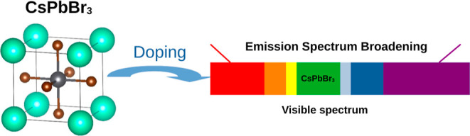
The atomic and electronic structures of perovskites are temperature-dependent. As the temperature rises, these materials often undergo structural phase transitions, typically evolving from orthorhombic to tetragonal and finally to cubic phases. , To broaden the scope of perovskite-based applications, for example, by extending the range of the absorption or emission spectra, it is necessary to tailor their electronic structures. One of the most effective strategies for achieving this is through compositional modification via doping. In a perovskite with the general formula ABX3, doping involves substituting atoms at the A, B, or X sites with alternative elements. In particular, heterovalent doping has been proposed as a means to enhance electrical conductivity and carrier mobility by introducing excess electron or hole carriers. , The change of electronic structure via doping also leads to a change in their optical properties. − Compared to double perovskites with the formula A2BB′X6, , doped perovskites exhibit higher absorption efficiency and photoluminescence quantum yield (PLQY), enhanced defect tolerance, low-cost fabrication, and tunable band gaps, making them particularly suitable for optoelectronic and solar cell applications. −
Substitution at the A-site has been proposed as a strategy to enhance the stability of perovskites, leading to higher PLQY and a reduction in surface defects. ,− For example, the substitution of Cs with Rb has been shown to improve structural stability by reducing Br vacancies, owing to lattice distortion that increases orbital coupling between Pb and Br.
Replacing Pb (at the B-site) is highly desirable because of its toxicity, provided that the optical performance is preserved or improved. Substitution at the B-site with elements such as Al, Ba, Ga, Mn, Ni, and Sn has been demonstrated to enhance PLQY, − increase emission lifetime, , improve power-conversion efficiency, raise the optical absorption coefficient, enhance stability, ,, and reduce surface defects.
Moreover, doping with certain elements (e.g., Ni as in ref ) can influence both radiative and nonradiative recombination pathways by passivating preexisting defects, such as vacancies. Nevertheless, prior theoretical investigations have indicated that substitution at the B-site is generally more challenging.
Atoms at the B- and X-sites play a critical role in determining the electronic and optical properties of perovskites, as they directly contribute to the valence-band maximum (VBM) and the conduction-band minimum (CBM). − For instance, the band gap has been shown to increase with the electronegativity of the B- and X-site atoms. Furthermore, both the band gap and the effective masses of charge carriers tend to decrease with increased orbital overlap, which can be achieved by doping with atoms that enlarge the Goldschmidt tolerance factormaking the structure more cubicor by selecting dopants with larger ionic radii at the X-site and smaller ionic radii at the A-site.
Doping with certain elements can lead to undesirable effects, such as a reduction in the emissive lifetime due to carrier trapping by defect states. For instance, doping with Sr2+ reduces the average PL lifetime from 200 ns to approximately 60 ns. Similarly, Bi3+ doping results in emission quenching by introducing trapping and scattering centers originating from defect states. In addition, intrinsic defects such as vacancies are generally detrimental to optoelectronic performance. Therefore, a comprehensive understanding of intrinsic defect formation and behavior is essential for improving device performance, as it enables the development of strategies to mitigate or eliminate these defects.
Many factors influence the phenomena observed in experiments, emphasizing the importance of theoretical studies for elucidating the underlying mechanisms. Establishing clear relationships between experimental observations and the atomic as well as electronic structures of perovskites provides critical physical insight. Although numerous theoretical works have investigated the effects of doping in perovskites, comprehensive studies at the atomic level remain limited. The objective of the present work is 2-fold. First, we aim to provide guidelines for tailoring the composition of halide perovskites toward specific applications by considering fundamental atomic properties (e.g., electronegativity and atomic radius) and their consequences for structural and electronic characteristics (e.g., bond lengths, lattice volume, band gap, dielectric response). Second, we seek to deepen the understanding of how atomic configurations govern electronic structure, thereby bridging experimental observations with theoretical insights.
In this work, we conduct a systematic investigation of the doping effects in CsPbBr3, considering a variety of dopants (including vacancies) at different crystallographic sites. We analyze the atomic properties, such as the formation energies of various dopants and their preferred configurations. The resulting electronic properties are examined through calculated band structures and densities of states (DOS). Additionally, we explore the influence of externally applied strain on the band structure of doped perovskites. Through this comprehensive study, we develop a general understanding of how different dopants impact both the atomic and electronic structures of CsPbBr3, offering insights that may be extended to other perovskite materials.
Computational Methods
Owing to computational limitations in evaluating the large number of dopants considered, only a single dopant is introduced into a 2 × 2 × 2 supercell of CsPbBr3 (containing 40 atoms) as an example (Figure ). This corresponds to doping concentrations of 12.5% for the A- and B-sites and 4.17% for the X-site. A variety of elements are considered as dopants: Na, K, and Rb for substitution at the A-site; Ag, Al, Ba, Bi, Ga, Mn, Na, Nb, Ni, and Sn at the B-site; and F, Cl, and I at the X-site. In addition, vacancy defects are modeled with 12.5% concentrations for Cs and Pb vacancies, and 4.17% for Br vacancies.
1.

Unit cell of doped CsPbBr3 perovskite at site (a) A (b) B (c) X. Cs, Pb, Br and dopant atoms are shown in green, gray, brown and red colors, respectively.
The Vienna Ab initio Simulation Package (VASP) − is employed for all calculations. The Perdew–Burke–Ernzerhof (PBE) exchange–correlation functional is used within the framework of the projector augmented-wave (PAW) method. , A k-point sampling grid of 4 × 4 × 4 is used for structural relaxation, while a denser grid of 10 × 10 × 10 is applied in the calculation of the density of states (DOS). For lower doping concentrations, 4 × 4 × 4 supercells (320 atoms) are employed, along with a 2 × 2 × 2 k-point mesh. These configurations correspond to doping concentrations of 1.56% at the A- and B-sites, and 0.52% at the X-site. The force convergence criterion for structural relaxation is set to 0.02 eV/atom, and the electronic minimization is performed until the total energy difference is less than 10–8 eV. Spin–orbit coupling (SOC) is included in all electronic structure calculations. It should be noted that all calculated band gaps are underestimated owing to the known limitations of the PBE functional. The atomic structures are visualized using VESTA, and the effective (unfolded) band structures are plotted using the VaspBandUnfolding code.
Owing to the excess charge remaining after substituting Pb2+ with monovalent ions (e.g., Ag and Na) or trivalent ions (e.g., Al, Bi, Ga, and Nb), the resulting doped perovskites are not charge-neutral. Therefore, a modified formation-energy expression for charged dopants is adopted −
| 1 |
where E T denotes the total energy of the doped system (Z:CsPbBr3) or pristine material (CsPbBr3); μ Z and μ Y are the chemical potentials of the added (Z) and removed (Y) atoms, respectively, in their elemental bulk forms; and n is the number of atoms of type Z replacing m atoms of type Y at the A-, B-, or X-sites. E VBM refers to the VBM of pristine CsPbBr3, and μe is the chemical potential of electrons (i.e., the Fermi level of undoped CsPbBr3 in this case), which can be varied within the band gap and treated as a tunable parameter. E corr is a correction term accounting for the finite-size effects and spurious electrostatic interactions of charged defects in supercell calculations (E corr of various doped CsPbBr3 are shown in Table S1). The formation energies of charged dopants are computed using the Spinney package.
Results and Discussion
Lattice Parameters in Different Doped CsPbBr3
Table presents various lattice parameters and formation energies for different doped CsPbBr3 systems. The Goldschmidt tolerance factor t is widely used as a preliminary indicator of structural stability
| 2 |
where r denotes the ionic radius of the atoms at the A, B, or X sites. The structure is considered thermodynamically stable if t lies between 0.8 and 1.0. , Within this range, the ions fit well into the cubic structure, minimizing strain energy. Most of the dopants examined in this work meet this criterion, with the notable exception of a Cs vacancy (VCs), which yields a smaller tolerance factor of t = 0.768. Additionally, the doped materials are found to satisfy the empirical bond-length relation , , where and denote the average bond lengths between atoms at the A (or B) and X sites, respectively. However, based on Table , the thermodynamic stability of a given dopant does not appear to correlate directly with the Goldschmidt tolerance factor. For instance, the Pb vacancy (VPb) exhibits a relatively high tolerance factor of t = 0.855 but also possesses a high formation energy of 5.12 eV. Other factors, such as configurational entropy, have also been shown to enhance the stability of halide perovskites. , Therefore, the tolerance factor alone is not sufficient to fully indicate structural stability.
1. Summary of Calculated Lattice Parameters for Various Doped CsPbBr3 Structures, Including Magnetic Moment (M), Lattice Constant (a), Average Bond Lengths (Cs–Br, Pb–Br, Cs–Pb), Volume Change After Doping (ΔV), Goldschmidt Tolerance Factor (t), and Doping Formation Energy (E F) .
| compound | M (μB) | a (Å) | Cs–Br | Pb–Br | Cs–Pb | ΔV (%) | t | E F (eV) |
|---|---|---|---|---|---|---|---|---|
| CsPbBr3 | 0.000 | 5.992 | 4.237 | 2.996 | 5.189 | 0.00 | 0.815 | |
| Na (A) | 0.000 | 5.985 | 4.241 | 2.993 | 5.185 | –0.34 | 0.797 | 1.73 |
| K (A) | 0.000 | 5.985 | 4.239 | 2.993 | 5.184 | –0.34 | 0.807 | 0.63 |
| Rb (A) | 0.000 | 5.986 | 4.235 | 2.993 | 5.184 | –0.29 | 0.811 | 0.41 |
| VCs (A) | 0.000 | 5.953 | 4.182 | 2.981 | 5.158 | –1.96 | 0.768 | 3.82 |
| Ag1+ (B) | 0.000 | 5.927 | 4.194 | 2.974 | 5.169 | –3.23 | 0.816 | 2.66 |
| Al3+ (B) | 0.000 | 5.936 | 4.200 | 3.014 | 5.153 | –2.80 | 0.837 | 1.76 |
| Ba (B) | 0.000 | 6.050 | 4.279 | 3.013 | 5.226 | 2.94 | 0.810 | –3.09 |
| Bi3+ (B) | 0.000 | 5.997 | 4.241 | 3.002 | 5.192 | 0.26 | 0.820 | 1.88 |
| Ga3+ (B) | 0.000 | 5.936 | 4.198 | 2.987 | 5.154 | –2.76 | 0.834 | 2.10 |
| Mn (B) | 4.400 | 5.930 | 4.194 | 2.994 | 5.154 | –3.09 | 0.829 | –7.64 |
| Na1+ (B) | 0.000 | 5.940 | 4.207 | 2.972 | 5.193 | –2.55 | 0.820 | 0.35 |
| Nb3+ (B) | 1.885 | 5.941 | 4.202 | 3.002 | 5.152 | –2.54 | 0.830 | 2.87 |
| Ni (B) | 1.380 | 5.915 | 4.186 | 2.998 | 5.152 | –3.80 | 0.831 | 3.00 |
| Sn (B) | 0.000 | 5.980 | 4.229 | 2.995 | 5.179 | –0.58 | 0.820 | 0.61 |
| VPb (B) | 0.000 | 5.927 | 4.204 | 2.956 | 5.200 | –3.23 | 0.855 | 5.12 |
| F (X) | 0.000 | 5.983 | 4.211 | 3.011 | 5.179 | –1.69 | 0.816 | –1.61 |
| Cl (X) | 0.000 | 5.995 | 4.229 | 2.994 | 5.180 | –0.53 | 0.815 | –0.20 |
| I (X) | 0.000 | 5.991 | 4.247 | 3.000 | 5.205 | 0.90 | 0.815 | 0.38 |
| IBr | 0.000 | 5.967 | 4.142 | 3.010 | 5.183 | –0.67 | 0.812 | –0.01 |
| VBr (X) | 0.000 | 6.015 | 4.234 | 3.000 | 5.198 | 0.37 | 0.818 | 3.32 |
Doping site positions are indicated in parentheses: (A) for site A, (B) for site B, and (X) for site X. Defects include Cs, Pb, and Br vacancies (VCs, VPb, VBr), and Br interstitials (IBr). Doping concentrations are 12.5% for sites A and B, and 4.17% for site X.
The volume of doped CsPbBr3 (within a 2 × 2 × 2 supercell) primarily depends on the distance between Cs and Br atoms, exhibiting an approximately linear relationship according to our calculations, as shown in Figure S1. For substitutions at the A-site, the formation energy increases with the resulting volume change, indicating that the formation energy is influenced by the ionic radius of the dopant occupying the A-site. The volume of doped CsPbBr3 is also correlated with the distance between the Pb atom and the substituted atom at the B-site (Figure S2). However, unlike the case of A-site substitution, the formation energy does not show a clear dependence on the volume in the case of B-site doping. Interestingly, substitution with certain elements such as Mn, Nb, and Ni at the B-site induces a net magnetic moment in the doped CsPbBr3, as summarized in Table . This observation is consistent with previous DFT calculations for Mn, and Ni. It should be noted that the PBE functional employed in this work affects the hybridization between atomic orbitals and underestimates the localization of the d orbitals in transition metals, resulting in reduced magnetic moments for CsPbBr3 doped with Mn, Ni, and Nb. For X-site substitutions, the formation energy tends to become more negative (indicating higher stability) with increasing electronegativity of the substituted atom. Specifically, the electronegativity trend follows F > Cl > I.
Na, the only element considered substituting at both A- and B-sites, shows a preference for replacing Pb (E F = 0.35 eV) over Cs (E F = 1.73 eV), consistent with previous theoretical work. This preference may be attributed to the reduction in bond lengths between Br and both Cs and Pb atoms. Substitution of Pb by Na introduces excess charge into the CsPbBr3 lattice. Na doping offers several benefits, including a reduction in Br vacancies, , enhancement of PLQY, , and improved stability under various environmental conditions. , The substitution site preference is influenced by the valence state and atomic radius of the alkali metal dopant, as well as the chemical potentials governed by the synthesis conditions.
Br vacancies (VBr) and Br interstitial doping result in volume expansion and compression, respectively. In contrast, both Pb vacancies (VPb) and Cs vacancies (VCs) lead to volume contraction. This behavior aligns with the redistribution of electronic charge around Pb atoms: charge depletion occurs in the presence of Cs and Pb vacancies, while Br vacancies result in charge accumulation. Among these, VBr is more likely to form (E F = 3.32 eV) than VCs (E F = 3.82 eV) and VPb (E F = 5.12 eV). The presence of VCs has been shown to cause local lattice distortions and reduce the photoluminescence (PL) lifetime. Mitigation strategies, such as adjusting the dosage of the Cs+ precursor, can suppress the formation of VCs.
For dopants exhibiting a net magnetic moment (e.g., Mn and Nb), the structure becomes more stable at higher doping concentrations. In practice, the likelihood of successfully forming doped CsPbBr3 also depends on experimental parameters, such as temperature, incident flux, and precursor ratios, which influence the local chemical potentials of the constituent atoms. Additionally, the kinetic processes occurring during synthesis play a critical role. ,
In addition, a clusterized dopant distribution is calculated to be more favorable for substitution at the A-site with elements from the same group as Cs in the periodic table. Substitutions at the B-site and X-site are more complex, as the dopant distributions are influenced by factors such as atomic radius and electronegativity. At the B-site, a clusterized dopant distribution is more favorable for dopants such as Ag, Bi, and Na, whereas an isolated distribution is preferred for Al, Ba, Ga, Mn, Nb, Ni, and Sn. At the X-site, clustering is favored for F and I, while Cl tends to adopt an isolated distribution. For vacancy defects, Cs vacancies are more likely to form in clusters, whereas Pb and Br vacancies tend to form in an isolated manner.
Electronic Properties in Different Doped CsPbBr3
Regardless of whether a dopant can be stably incorporated into CsPbBr3, it is informative to examine how these dopants influence the electronic band structure. The effective (unfolded) band structures of pristine and doped CsPbBr3 are shown in Figures and , with the corresponding band gaps summarized in Table S2. In this work, we focus only on the relative changes in the band gap of doped CsPbBr3 compared to pristine CsPbBr3. This choice is motivated by the well-known underestimation of band gaps obtained using the PBE functional. For instance, the experimental band gap of pristine CsPbBr3 is 2.3 eV, , whereas our calculations yield 1.78 eV without SOC and 0.64 eV with SOC, consistent with previous theoretical reports. ,,
2.

(a) Band structure and (b) partial density of states of pristine CsPbBr3.
3.

Effective band structures of various doped CsPbBr3 within 2 × 2 × 2 supercells: (a) Na0.125Cs0.875PbBr3, (b) K0.125Cs0.875PbBr3, (c) Rb0.125Cs0.875PbBr3, (d) 12.5% Cs vacancy, (e) CsNa0.125Pb0.875Br3, (f) CsBa0.125Pb0.875Br3, (g) CsGa0.125Pb0.875Br3, (h) 12.5% Pb vacancy, (i) CsPbF0.042Br0.958, (j) CsPbCl0.042Br0.958, (k) CsPbI0.042Br0.958, and (l) 4.17% Br vacancy. The Fermi energy is aligned to 0 eV, and spin–orbit coupling is included in all calculations.
For dopants substituting Cs at the A-site, as shown in Figure a–d, elements such as K, Na, and Rblocated in the same group (column) as Cs in the periodic tabledo not significantly alter the overall characteristics of the band structure compared to pristine CsPbBr3. The trend of decreasing band gap with increasing ionic radius of the A-site dopant, when considering the SOC effect (see Table S2), is consistent with the results reported in ref This behavior can be attributed to the fact that the electronic states of Cs and its group-equivalent dopants contribute minimally to the VBM and CBM, as illustrated in Figures and S4. From a structural perspective, the bond distances between Cs and neighboring atoms (i.e., Pb and Br) are larger than those between Pb and Br (see Table ), further supporting the minimal impact of A-site dopants on the electronic band structure.
Substitution at the B-site leads to more pronounced changes in the band structure, except in the case of Sn, which belongs to the same group as Pb in the periodic table (see Figures and S3). In particular, the presence of defect states results in a metallic character (i.e., zero band gap) for Ga-substitution at the B-site [Figure g]. Similar defect states are observed for other dopants, though their orbital origins vary. For example, the defect states arise from d orbitals in the case of Ni [Figure S5f] and Nb [Figure S5i], and from p orbitals in the case of Bi [Figure S5g]. As shown in the plots of the partial density of states (PDOS) in Figure S5f–i, these dopants significantly alter the density of states near the VBM and CBM. In Figure , it is evident that the influence of these defect states becomes less pronounced at lower doping concentrations (1.56%). This trend aligns with previous theoretical work, which demonstrated that Nb-doped CsPbBr3 can exhibit either metallic or semiconducting behavior depending on the doping concentration [see Figure c,g].
4.

Comparison of effective band structures of B-site-doped CsPbBr3 at different substitution concentrations: (a) CsBi0.125Pb0.875Br3, (b) CsMn0.125Pb0.875Br3, (c) CsNb0.125Pb0.875Br3, (d) CsNi0.125Pb0.875Br3, (e) CsBi0.016Pb0.984Br3, (f) CsMn0.016Pb0.984Br3, (g) CsNb0.016Pb0.984Br3, (h) CsNi0.016Pb0.984Br3. The Fermi energy is aligned to 0 eV and spin–orbit coupling is not included.
The origin of these defect states is illustrated in Figure S7, based on the atomic energy levels of the dopant and host atoms. The in-gap defect states observed in the band structures of charged dopants (i.e., those with valency 1+ or 3+) arise from dopant atomic energy levels that lie within the energy range spanned by the Br 4p and Pb 6p orbitals, which primarily contribute to the VBM and CBM in pristine CsPbBr3. It is worth noting that although the Ga 4s orbital lies outside this energy range in the isolated atom, it still gives rise to in-gap defect states due to significant changes in the band structure after doping. These changes result in a downward shift of the Ga 4s orbital energy, placing it within the gap.
Changes in the band gap (see Table S2 for values without spin–orbit coupling) are influenced not only by the appearance of in-gap defect states, but also by the alignment of dopant atomic energy levels relative to the Pb 6p and Br 4p orbitals. For example, dopants such as Mn and Ni at the B-site have energy levels close to those of Pb orbitals, while dopants such as Al, Bi, and Sn at the B-site, and F, Cl, and I at the X-site, possess orbital characters similar to the VBM or CBM, which also affect the band edges.
The incorporation of monovalent dopants (1+ ions), such as Na and Ag (which have one fewer valence electron than Pb2+) leads to a downward shift for the Fermi energy to a lower energy relative to pristine CsPbBr3. In these doped CsPbBr3, the states above the shifted Fermi energy 0 eV (which resemble the VBM of pristine CsPbBr3) are unoccupied. A similar observation was reported in previous experimental work on Ag-doped CsPbBr3, where strong p-type character was observed. In contrast, trivalent dopants (3+ ions), such as Al, Bi, and Nb (which have one more valence electron than Pb2+), induce an upward shift of the Fermi energy relative to pristine CsPbBr3, bringing the CBM of pristine CsPbBr3 closer to 0 eV. Depending on the orbital composition of the dopant, the states near 0 eV originate from different orbitals: s orbitals for Al [Figure S5j], p orbitals for Bi [Figure S5g], and d orbitals for Nb [Figure S5i].
For charge-neutral dopants such as Ba and Mn, the orbital contributions near 0 eV differ: in Ba-doped CsPbBr3, they stem from the s and p orbitals of Pb (Figure S5d), while in Mn-doped CsPbBr3, they originate from Mn d orbitals (Figure S5e). PLQY enhancement in Mn-doped CsPbBr3 has been attributed to d–d transitions in Mn2+, facilitated by energy transfer from excitons. , Kanoun and Goumri-Said. also reported other advantages of Mn doping, such as suppression of defect states and increased carrier effective masses. The latter is consistent with the localized nature of Mn d orbitals observed in the PDOS [Figure S5e]. These findings suggest that doping with elements possessing d orbitals may be an effective strategy for modulating carrier effective masses in perovskite materials. The corresponding PDOS for various B-site doped CsPbBr3 systems are shown in Figure S5.
For substitution at the X-site, the band structures of CsPbBr3 doped with F, Cl, and I remain largely similar to that of pristine CsPbBr3, as these dopants belong to the same group as Br in the periodic table [Figure i–k]. In contrast, doping Br at an interstitial site induces defect states near 0 eV [Figure S3h]. These defect states primarily originate from the p orbitals of the interstitial Br atom [Figure S6d], consistent with the orbital character of the VBM in pristine CsPbBr3. Notably, the energy position of these defect states can shift slightly upward or downward, depending on the precise interstitial location of the Br atom.
As shown in Figure d,h,l, vacancies of Cs and Pb exhibit opposite effects on the band structure compared to Br vacancies. Specifically, Cs and Pb vacancies shift the Fermi energy (0 eV) downward, while Br vacancies shift the Fermi energy (0 eV) upward relative to pristine CsPbBr3. This behavior arises from the electron count imbalance: Cs and Pb vacancies result in a deficiency of valence electrons, making it difficult to fully occupy the original VBM; conversely, Br vacancies introduce extra electrons that partially fill the CBM.
The emergence of defect states induces significant modifications in the dielectric function. Figure presents the dielectric functions of various doped CsPbBr3 systems. Charge-neutral dopants at the A- and X-sites generally induce minimal changes [Figure a,b,e,f]. In contrast, B-site doping typically causes a shift of the peaks around 3.5 eV toward lower energies [Figure c,d]. Charged dopants result in more pronounced modifications to the dielectric functions, including the emergence of peaks below 1 eV [Figure g,i] and noticeable changes in the magnitude of the dielectric response [Figure h,j].
5.

Dielectric functions of doped perovskites within 2 × 2 × 2 supercells. Imaginary dielectric functions ϵi of defects at site (a) A (charged-neutral), (c) B (charged-neutral), (e) X (charged-neutral), (g) B (1+ ions), (i) B (3+ ions). Real dielectric functions ϵr of defects at site (b) A (charged-neutral) (d) B (charged-neutral), (f) X (charged-neutral), (h) B (1+ ions), (j) B (3+ ions).
On the other hand, the influence of dopant distribution on the band structure can also be investigated. In this case, the doping concentration is increased to 25.0% for substitutions at the A- and B-sites, and 8.3% for substitutions at the X-site, corresponding to two dopants introduced into a 2 × 2 × 2 supercell. As shown in Figure , the dopant distributions of Na and F at the A- and X-sites, respectively, do not significantly alter the overall characteristics of the band structures [Figure a,d,e,h]. For substitutions at the A- and X-sites, the resulting band gap of doped CsPbBr3 is generally larger when the dopants are arranged in a clusterized configuration. In contrast, for substitutions at the B-site, isolated dopant distributions (Table S3) tend to produce wider band gaps compared to their clusterized counterparts [Figure b,c,f,g]. For doped CsPbBr3 exhibiting a net magnetic moment, the magnetic moment increases only slightly in clusterized dopant distributions compared to isolated ones. The magnetic moment and the nature of ferromagnetic or antiferromagnetic couplings in clusterized distributions may vary depending on the choice of transition metal dopants or the doping concentration.
6.

Comparison of effective band structures of doped CsPbBr3 with different dopant distributions, calculated using 2 × 2 × 2 supercells. (a) Na0.250Cs0.750PbBr3 with a clusterized dopant distribution; (b) CsBa0.250Pb0.750Br3 with a clusterized dopant distribution; (c) CsMn0.250Pb0.750Br3 with a clusterized dopant distribution; (d) CsPbF0.084Br0.916 with a clusterized dopant distribution; (e) Na0.250Cs0.750PbBr3 with an isolated dopant distribution; (f) CsBa0.250Pb0.750Br3 with an isolated dopant distribution; (g) CsMn0.250Pb0.750Br3 with an isolated dopant distribution; (h) CsPbF0.084Br0.916 with an isolated dopant distribution. The Fermi energy is aligned to 0 eV in all panels, and spin–orbit coupling is included.
Since dopant distribution also affects the band structure, the optoelectronic properties, which are determined by electronic parameters such as the band gap, effective mass, and Kane parameter (describing the interaction between valence and conduction bands), can vary with different dopant configurations. Clustered dopant distributions are predicted to have larger effects, such as enhanced orbital overlap and the formation of impurity bands, because strengthened dopant interactions induce more significant changes in the electronic structure. For example, the PLQY of CsPbBr3 nearly doubles due to quantum cutting when Yb atoms occupy neighboring B-site positions. −
The change in band structure depends primarily on electronic effects rather than geometrical ones. Na0.125Cs0.875PbBr3, CsBa0.125Pb0.875Br3, and CsPbI0.042Br0.958 lead to volume changes of −0.34%, +2.94%, and +0.90%, respectively, compared to pristine CsPbBr3. The corresponding band gaps are modified to E g = 0.694, 1.096, and 0.664 eV, in contrast to E g ≈ 0.637 eV for pristine CsPbBr3. When external strain is applied in the reverse direction of the volume change, the band gap does not return to its original value. Instead, it shifts to 0.728, 0.834, and 0.570 eV, respectively. The corresponding band structures under external strain are shown in Figure . The direction of applied strain successfully restores the band gap for substitution with Ba (at the B-site) and I (at the X-site), but not for substitutions with Na (at the A-site). In general, the band gap of a doped perovskite increases under tensile strain and decreases under compressive strain (see Figure S8), in agreement with previous theoretical studies. This behavior arises because compressive and tensile strains, respectively, increase and decrease the orbital overlap and hybridization in the VBM and CBM, thereby altering the band gap.
7.

Effective band structures of doped CsPbBr3 perovskites within 2 × 2 × 2 supercells under externally applied strain. (a) Na0.125Cs0.875PbBr3 under 0.34% tensile strain; (b) CsBa0.125Pb0.875Br3 under 2.94% compressive strain; (c) CsPbI0.042Br0.958 under 0.90% compressive strain. The Fermi energy is aligned to 0 eV in all panels, and spin–orbit coupling is included.
Conclusion
In this work, we investigate the atomic and electronic structures of various doped CsPbBr3 perovskites. The thermodynamic stability of dopants is influenced by both their electronegativity and ionic radius, particularly for B- and X-site substitutions. The unit cell volume increases when atoms are removed from the X site, but decreases for removal at the A or B sites or for interstitial doping at X. A tendency toward dopant cluster formation is observed only for A-site substitutions. While A-site doping has little effect on the band structure, dopants at B and X sites can induce significant changes, including the emergence of defect states, modifications to the band gap, effective mass, and dielectric functions. Additionally, the dopant distribution and externally applied strain can further modulate the electronic structure of doped CsPbBr3.
Supplementary Material
Acknowledgments
The authors would like to thank the CEA’s PTC-MP program and GENCI project AD010914188 for support.
The Supporting Information is available free of charge at https://pubs.acs.org/doi/10.1021/acsomega.5c07761.
Volume versus average Cs–Br distance; volume versus average Pb-dopant distance at the B-site; effective band structures of various doped CsPbBr3 systems; partial density of states (PDOS) of selected doped configurations; atomic energy levels of various elements in PAW–PBE pseudopotentials; band structures under applied external strain; tabulated values of E corr for different charged dopants; tabulated values of band gap for various dopants with and without SOC; and band gap for different dopant distributions (PDF)
†.
Department of Physics, National University of Singapore, 2 Science Drive 3, Singapore 117542, Singapore
The authors declare no competing financial interest.
References
- Xu J., Huang W., Li P., Onken D. R., Dun C., Guo Y., Ucer K. B., Lu C., Wang H., Geyer S. M., Williams R. T., Carroll D. L.. Imbedded nanocrystals of CsPbBr3 in Cs4PbBr6: kinetics, enhanced oscillator strength, and application in light-emitting diodes. Adv. Mater. 2017;29:1703703. doi: 10.1002/adma.201703703. [DOI] [PubMed] [Google Scholar]
- Li G., Tan Z.-K., Di D., Lai M. L., Jiang L., Lim J. H.-W., Friend R. H., Greenham N. C.. Efficient light-emitting diodes based on nanocrystalline perovskite in a dielectric polymer matrix. Nano Lett. 2015;15:2640–2644. doi: 10.1021/acs.nanolett.5b00235. [DOI] [PubMed] [Google Scholar]
- Shen K., Li X., Xu H., Wang M., Dai X., Guo J., Zhang T., Li S., Zou G., Choy K.-L., Parkin I. P., Guo Z., Liu H., Wu J.. Enhanced performance of ZnO nanoparticle decorated all-inorganic CsPbBr3 quantum dot photodetectors. J. Mater. Chem. A. 2019;7:6134–6142. doi: 10.1039/C9TA00230H. [DOI] [Google Scholar]
- Fang Y., Huang J.. Resolving weak light of sub-picowatt per square centimeter by hybrid perovskite photodetectors enabled by noise reduction. Adv. Mater. 2015;27:2804–2810. doi: 10.1002/adma.201500099. [DOI] [PubMed] [Google Scholar]
- Pan J., Sarmah S. P., Murali B., Dursun I., Peng W., Parida M. R., Liu J., Sinatra L., Alyami N., Zhao C., Alarousu E., Ng T. K., Ooi B. S., Bakr O. M., Mohammed O. F.. Air-Stable Surface-passivated perovskite quantum dots for ultra-robust, single- and two-photon-induced amplified spontaneous emission. J. Phys. Chem. Lett. 2015;6:5027–5033. doi: 10.1021/acs.jpclett.5b02460. [DOI] [PubMed] [Google Scholar]
- Zhu H., Fu Y., Meng F., Wu X., Gong Z., Ding Q., Gustafsson M. V., Trinh M. T., Jin S., Zhu X.-Y.. Lead halide perovskite nanowire lasers with low lasing thresholds and high quality factors. Nat. Mater. 2015;14:636–642. doi: 10.1038/nmat4271. [DOI] [PubMed] [Google Scholar]
- Zhou D., Liu D., Pan G., Chen X., Li D., Xu W., Bai X., Song H.. Cerium and ytterbium codoped halide perovskite quantum dots: a novel and efficient downconverter for improving the performance of silicon solar cells. Adv. Mater. 2017;29:1704149. doi: 10.1002/adma.201704149. [DOI] [PubMed] [Google Scholar]
- Zhao Q., Hazarika A., Chen X., Harvey S. P., Larson B. W., Teeter G. R., Liu J., Song T., Xiao C., Shaw L., Zhang M., Li G., Beard M. C., Luther J. M.. High efficiency perovskite quantum dot solar cells with charge separating heterostructure. Nat. Commun. 2019;10:2842. doi: 10.1038/s41467-019-10856-z. [DOI] [PMC free article] [PubMed] [Google Scholar]
- Blundell S. A., Guet C.. All-order correlation of single excitons in nanocrystals using a k.p envelope-function approach: Application to lead halide perovskites. Phys. Rev. B. 2022;105:155420. doi: 10.1103/PhysRevB.105.155420. [DOI] [Google Scholar]
- Nguyen T. P. T., Blundell S. A., Guet C.. One-photon absorption by inorganic perovskite nanocrystals: A theoretical study. Phys. Rev. B. 2020;101:195414. doi: 10.1103/PhysRevB.101.195414. [DOI] [Google Scholar]
- Hoffman A. E. J., Saha R. A., Borgmans S., Puech P., Braeckevelt T., Roeffaers M. B. J., Steele J. A., Hofkens J., Van Speybroeck V.. Understanding the phase transition mechanism in the lead halide perovskite CsPbBr3 via theoretical and experimental GIWAXS and Raman spectroscopy. APL Mater. 2023;11:041124. doi: 10.1063/5.0144344. [DOI] [Google Scholar]
- Hussain M., Rashid M., Saeed F., Bhatti A. S.. Spin–orbit coupling effect on energy level splitting and band structure inversion in CsPbBr3 . J. Mater. Sci. 2021;56:528–542. doi: 10.1007/s10853-020-05298-8. [DOI] [Google Scholar]
- Zhang J., Di Q., Liu J., Bai B., Liu J., Xu M., Liu J.. Heterovalent doping in colloidal semiconductor nanocrystals: cation-exchange-enabled new accesses to tuning dopant luminescence and electronic impurities. J. Phys. Chem. Lett. 2017;8:4943–4953. doi: 10.1021/acs.jpclett.7b00351. [DOI] [PubMed] [Google Scholar]
- Mcmeekin D. P., Sadoughi G., Rehman W., Eperon G. E., Saliba M., Hörantner M. T., Haghighirad A., Sakai N., Korte L., Rech B., Johnston M. B., Herz L. M., Snaith H. J.. A mixed-cation lead mixed-halide perovskite absorber for tandem solar cells. Science. 2016;351:151–155. doi: 10.1126/science.aad5845. [DOI] [PubMed] [Google Scholar]
- Lin C., Xue Y., Persson C., Huang D.. Theoretical optimization of an earth-abundant and environmentally friendly photovoltaic absorber Cu3PSe4 from first-principles study to device simulation. ACS Appl. Mater. Interfaces. 2024;16:52252–52263. doi: 10.1021/acsami.4c10113. [DOI] [PubMed] [Google Scholar]
- Xue Y., Lin C., Zhong J., Huang D., Persson C.. Group-IIIA element doped BaSnS2 as a high efficiency absorber for intermediate band solar cell from a first-principles insight. Phys. Chem. Chem. Phys. 2024;26:8380–8389. doi: 10.1039/D3CP05824G. [DOI] [PubMed] [Google Scholar]
- Xue Y., Lin C., Huang B., He H., Huang D., Persson C.. A theoretical investigation on the structure stability, electronic structures, optical properties, and transport properties of Zintl compounds CsZn4P3 and CsZn4As3 . J. Solid State Chem. 2024;339:124976. doi: 10.1016/j.jssc.2024.124976. [DOI] [Google Scholar]
- Xue Y., Lin C., Huang Y., Zhang S., Zhong J., Huang D.. Sb-doped β-SrZrS3 as a low-toxic and low-priced absorber for intermediate band solar cells: A first-principles investigation. Phys. B. 2023;658:414839. doi: 10.1016/j.physb.2023.414839. [DOI] [Google Scholar]
- Kumari S., Bairwa J. K.. Exploring halide double perovskites for enhanced efficiency in photovoltaic application. Radius J. Sci. Technol. 2024;1:241002. doi: 10.5281/zenodo.14990283. [DOI] [Google Scholar]
- Bairwa J. K., Kumari S.. Oxide double perovskites: bridging the gap in photovoltaic and thermoelectric applications. Radius J. Sci. Technol. 2024;1:241004. [Google Scholar]
- Guan M., Xie Y., Wang Y., He Z., Qiu L., Liu J., Chen K., Yan S., Li G., Dai Z.. Enhanced emission efficiency in doped CsPbBr3 perovskite nanocrystals: the role of ion valence. J. Mater. Chem. C. 2022;10:14737–14745. doi: 10.1039/D2TC03442E. [DOI] [Google Scholar]
- Wang D., Li W., Du Z., Li G., Sun W., Wu J., Lan Z.. CoBr2-doping-induced efficiency improvement of CsPbBr3 planar perovskite solar cells. J. Mater. Chem. C. 2020;8:1649–1655. doi: 10.1039/C9TC05679C. [DOI] [Google Scholar]
- Deng Y., Ni Z., Palmstrom A. F., Zhao J., Xu S., Van Brackle C. H., Xiao X., Zhu K., Huang J.. Reduced self-doping of perovskites induced by short annealing for efficient solar modules. Joule. 2020;4:1949–1960. doi: 10.1016/j.joule.2020.07.003. [DOI] [Google Scholar]
- Zhang C., Ding S., Liu G., He D., Chen P., Wu W.-Q., Wang L.. Metal-doping for perovskite optoelectronic applications. Mater. Today. 2025;89:172–191. doi: 10.1016/j.mattod.2025.07.010. [DOI] [Google Scholar]
- Huang S., Wang B., Zhang Q., Li Z., Shan A., Li L.. Postsynthesis potassium-modification method to improve stability of CsPbBr3 perovskite nanocrystals. Adv. Mater. 2018;6:1701106. doi: 10.1002/adom.201701106. [DOI] [Google Scholar]
- Yang J.-N., Song Y., Yao J.-S., Wang K.-H., Wang J.-J., Zhu B.-S., Yao M.-M., Rahman S. U., Lan Y.-F., Fan F.-J., Yao H.-B.. Potassium bromide surface passivation on CsPbI3 – xBrx nanocrystals for efficient and stable pure red perovskite light-emitting diodes. J. Am. Chem. Soc. 2020;142:2956–2967. doi: 10.1021/jacs.9b11719. [DOI] [PubMed] [Google Scholar]
- Kim D., Jo Y.-R., Kim S., Yim S.-Y., Lee J.-H., Lee C.-L.. Investigation of potassium doping and defect healing mechanism in core–shell CsPbBr3/SiO2 quantum dots. J. Mater. Chem. C. 2024;12:6395–6405. doi: 10.1039/D4TC00537F. [DOI] [Google Scholar]
- Bai T., Wang S., Zhang W., Yi L.. Vacuum evaporation deposited RbxCs1 – xPbBr3 thin films for spectrally tunable and stable all-inorganic blue light-emitting diodes. Mater. Sci. Semicond. Process. 2025;186:109085. doi: 10.1016/j.mssp.2024.109085. [DOI] [Google Scholar]
- Zeng F., Tan Y., Hu W., Tang X., Zhang X., Yin H.. A facile strategy to synthesize high colour purity blue luminescence aluminium-doped CsPbBr3 perovskite quantum dots. J. Lumin. 2022;245:118788. doi: 10.1016/j.jlumin.2022.118788. [DOI] [Google Scholar]
- Mei E., Chen Y., Chen Y., He Q., Tong Y., Yu P., Liang X., Xiang W.. Ba-doped CsPbBr3 with high quantum efficiency for wide color gamut on white light-emitting diodes. Appl. Phys. Lett. 2021;119:251103. doi: 10.1063/5.0070326. [DOI] [Google Scholar]
- Jiang M., Pan C.-Y.. Research on the stability of luminescence of CsPbBr3 and Mn:CsPbBr3 PQDs in polar solution. RSC Adv. 2022;12:15420–15426. doi: 10.1039/D2RA02165J. [DOI] [PMC free article] [PubMed] [Google Scholar]
- Wang J., Xu Y., Zou S., Pang C., Cao R., Pan Z., Guo C., Hu S., Liu J., Xie Z., Gong Z.. Effective defect passivation of CsPbBr3 quantum dots using gallium cations toward the fabrication of bright perovskite LEDs. J. Mater. Chem. C. 2021;9:11324–11330. doi: 10.1039/D1TC01077H. [DOI] [Google Scholar]
- Zhang M., Han X., Yang C., Zhang G., Guo W., Li J., Chen Z., Li B., Chen R., Qin C., Hu J., Yang Z., Zeng G., Xiao L., Jia S.. Size uniformity of CsPbBr3 perovskite quantum dots via manganese-doping. Nanomaterials. 2024;14:1284. doi: 10.3390/nano14151284. [DOI] [PMC free article] [PubMed] [Google Scholar]
- Ji S., Yuan X., Zheng J., Cao S., Ji W., Li H., Zhao J., Zhang H.. Near-unity blue-orange dual-emitting Mn-doped perovskite nanocrystals with metal alloying for efficient white light-emitting diodes. J. Colloid Interface Sci. 2021;603:864–873. doi: 10.1016/j.jcis.2021.06.138. [DOI] [PubMed] [Google Scholar]
- Shapiro A., Heindl M. W., Horani F., Dahan M.-H., Tang J., Amouyal Y., Lifshitz E.. Significance of Ni doping in CsPbX3 nanocrystals via postsynthesis cation–anion coexchange. J. Phys. Chem. C. 2019;123:24979–24987. doi: 10.1021/acs.jpcc.9b08317. [DOI] [Google Scholar]
- Vitoreti A. B. F., Agouram S., Solis de la Fuente M., Muñoz-Sanjosé V., Schiavon M. A., Mora-Seró I.. Study of the partial substitution of Pb by Sn in Cs–Pb–Sn–Br nanocrystals owing to obtaining stable nanoparticles with excellent optical properties. J. Phys. Chem. C. 2018;122:14222–14231. doi: 10.1021/acs.jpcc.8b02499. [DOI] [PMC free article] [PubMed] [Google Scholar]
- Yang Z., Yuan X., Song Y., Chen M., Xing K., Cao S., Zheng J., Zhao J.. Thickness-dependent photoluminescence properties of Mn-doped CsPbBr3 perovskite nanoplatelets synthesized at room temperature. J. Phys. Chem. C. 2023;127:21227–21234. doi: 10.1021/acs.jpcc.3c05639. [DOI] [Google Scholar]
- Wang G., Bi J., Chang J., Lei M., Zheng H., Yan Y.. Bandgap tuning of a CsPbBr3 perovskite with synergistically improved quality via Sn2+ doping for high-performance carbon-based inorganic perovskite solar cells. Inorg. Chem. Front. 2022;9:4359–4368. doi: 10.1039/D2QI00802E. [DOI] [Google Scholar]
- Liu D., Peng H., Sa R.. The structural, electronic and optical properties of all-inorganic CsPb1 – xSnxBr3 perovskite: A theoretical study. Comput. Theor. Chem. 2021;1205:113444. doi: 10.1016/j.comptc.2021.113444. [DOI] [Google Scholar]
- Zou S., Liu Y., Li J., Liu C., Feng R., Jiang F., Li Y., Song J., Zeng H., Hong M., Chen X.. Stabilizing cesium lead halide perovskite lattice through Mn(II) substitution for air-stable light-emitting diodes. J. Am. Chem. Soc. 2017;139:11443–11450. doi: 10.1021/jacs.7b04000. [DOI] [PubMed] [Google Scholar]
- Chen Q., Chen L., Shuai W., Miao B.. High entropy enhanced phase & structural stability and high electromagnetic wave absorption in CsPbBr3 perovskite. Mater. Sci. Semicond. Process. 2024;175:108295. doi: 10.1016/j.mssp.2024.108295. [DOI] [Google Scholar]
- Yong Z.-J., Guo S.-Q., Ma J.-P., Zhang J.-Y., Li Z.-Y., Chen Y.-M., Zhang B.-B., Zhou Y., Shu J., Gu J.-L., Zheng L.-R., Bakr O. M., Sun H.-T.. Doping-enhanced short-range order of perovskite nanocrystals for near-unity violet luminescence quantum yield. J. Am. Chem. Soc. 2018;140:9942–9951. doi: 10.1021/jacs.8b04763. [DOI] [PubMed] [Google Scholar]
- Parobek D., Roman B. J., Dong Y., Jin H., Lee E., Sheldon M., Son D. H.. Exciton-to-dopant energy transfer in Mn-doped cesium lead halide perovskite nanocrystals. Nano Lett. 2016;16:7376–7380. doi: 10.1021/acs.nanolett.6b02772. [DOI] [PubMed] [Google Scholar]
- Eperon G. E., Ginger D. S.. B-site metal cation exchange in halide perovskites. ACS Energy Lett. 2017;2:1190–1196. doi: 10.1021/acsenergylett.7b00290. [DOI] [Google Scholar]
- Ezzeldien M., Al-Qaisi S., Alrowaili Z. A., Alzaid M., Maskar E., Es-Smairi A., Vu T. V., Rai D. P.. Electronic and optical properties of bulk and surface of CsPbBr3 inorganic halide perovskite a first principles DFT 1/2 approach. Sci. Rep. 2021;11:20622. doi: 10.1038/s41598-021-99551-y. [DOI] [PMC free article] [PubMed] [Google Scholar]
- Islam M. N., Hadi M. A., Podder J.. Influence of Ni doping in a lead-halide and a lead-free halide perovskites for optoelectronic applications. AIP Adv. 2019;9:125321. doi: 10.1063/1.5132985. [DOI] [Google Scholar]
- Ghaithan H. M., Alahmed Z. A., Qaid S. M. H., Hezam M., Aldwayyan A. S.. Density functional study of cubic, tetragonal, and orthorhombic CsPbBr3 perovskite. ACS Omega. 2020;5:7468–7480. doi: 10.1021/acsomega.0c00197. [DOI] [PMC free article] [PubMed] [Google Scholar]
- Castelli I. E., García-Lastra J. M., Thygesen K. S., Jacobsen K. W.. Bandgap calculations and trends of organometal halide perovskites. APL Mater. 2014;2:081514. doi: 10.1063/1.4893495. [DOI] [Google Scholar]
- Ashari-Astani N., Meloni S., Salavati A. H., Palermo G., Grätzel M., Rothlisberger U.. Computational characterization of the dependence of halide perovskite effective masses on chemical composition and structure. J. Phys. Chem. C. 2017;121:23886–23895. doi: 10.1021/acs.jpcc.7b04898. [DOI] [Google Scholar]
- Shai X., Zuo L., Sun P., Liao P., Huang W., Yao E.-P., Li H., Liu S., Shen Y., Yang Y., Wang M.. Efficient planar perovskite solar cells using halide Sr-substituted Pb perovskite. Nano Energy. 2017;36:213–222. doi: 10.1016/j.nanoen.2017.04.047. [DOI] [Google Scholar]
- Begum R., Parida M. R., Abdelhady A. L., Murali B., Alyami N. M., Ahmed G. H., Hedhili M. N., Bakr O. M., Mohammed O. F.. Engineering interfacial charge transfer in CsPbBr3 perovskite nanocrystals by heterovalent doping. J. Am. Chem. Soc. 2017;139:731–737. doi: 10.1021/jacs.6b09575. [DOI] [PubMed] [Google Scholar]
- Guo Z., Yuan M., Chen G., Liu F., Lu R., Yin W.-J.. Understanding defects in perovskite solar cells through computation: current knowledge and future challenge. Adv. Sci. 2024;11:2305799. doi: 10.1002/advs.202305799. [DOI] [PMC free article] [PubMed] [Google Scholar]
- Kresse G., Hafner J.. Ab initio molecular dynamics for liquid metals. Phys. Rev. B: Condens. Matter Mater. Phys. 1993;47:558–561. doi: 10.1103/physrevb.47.558. [DOI] [PubMed] [Google Scholar]
- Kresse G., Hafner J.. Ab initio molecular-dynamics simulation of the liquid-metal-amorphous-semiconductor transition in germanium. Phys. Rev. B: Condens. Matter Mater. Phys. 1994;49:14251. doi: 10.1103/PhysRevB.49.14251. [DOI] [PubMed] [Google Scholar]
- Kresse G., Furthmüller J.. Efficiency of ab-initio total energy calculations for metals and semiconductors using a plane-wave basis set. Comput. Mater. Sci. 1996;6:15–50. doi: 10.1016/0927-0256(96)00008-0. [DOI] [PubMed] [Google Scholar]
- Kresse G., Furthmüller J.. Efficient iterative schemes for ab initio total-energy calculations using a plane-wave basis set. Phys. Rev. B: Condens. Matter Mater. Phys. 1996;54:11169. doi: 10.1103/PhysRevB.54.11169. [DOI] [PubMed] [Google Scholar]
- Perdew J. P., Burke K., Ernzerhof M.. Generalized gradient approximation made simple. Phys. Rev. Lett. 1996;77:3865. doi: 10.1103/PhysRevLett.77.3865. [DOI] [PubMed] [Google Scholar]
- Blöchl P. E.. Projector augmented-wave method. Phys. Rev. B: Condens. Matter Mater. Phys. 1994;50:17953. doi: 10.1103/PhysRevB.50.17953. [DOI] [PubMed] [Google Scholar]
- Kresse G., Joubert D.. From ultrasoft pseudopotentials to the projector augmented-wave method. Phys. Rev. B: Condens. Matter Mater. Phys. 1999;59:1758. doi: 10.1103/PhysRevB.59.1758. [DOI] [Google Scholar]
- Momma K., Izumi F.. VESTA3 for three-dimensional visualization of crystal, volumetric and morphology data. J. Appl. Crystallogr. 2011;44:1272–1276. doi: 10.1107/S0021889811038970. [DOI] [Google Scholar]
- https://github.com/QijingZheng/VaspBandUnfolding (accessed November 2024).
- Freysoldt C., Grabowski B., Hickel T., Neugebauer J., Kresse G., Janotti A., Van de Walle C. G.. First-principles calculations for point defects in solids. Rev. Mod. Phys. 2014;86:253. doi: 10.1103/RevModPhys.86.253. [DOI] [Google Scholar]
- https://docs.quantumatk.com/tutorials/charged_defects/charged_defects.html (accessed November 2024).
- Freysoldt C., Lange B., Neugebauer J., Yan Q., Lyons J. L., Janotti A., Van de Walle C. G.. Electron and chemical reservoir corrections for point defect formation energies. Phys. Rev. B. 2016;93:165206. doi: 10.1103/PhysRevB.93.165206. [DOI] [Google Scholar]
- Ramprasad R., Zhu H., Rinke P., Scheffler M.. New perspective on formation energies and energy levels of point defects in nonmetals. Phys. Rev. Lett. 2012;108:066404. doi: 10.1103/PhysRevLett.108.066404. [DOI] [PubMed] [Google Scholar]
- Bajaj S., Pomrehn G. S., Doak J. W., Gierlotka W., Wu H.-J., Chen S.-W., Wolverton C., Goddard W. A. III, Jeffrey Snyder G.. Ab initio study of intrinsic point defects in PbTe: an insight into phase stability. Acta Mater. 2015;92:72–80. doi: 10.1016/j.actamat.2015.03.034. [DOI] [Google Scholar]
- https://gitlab.com/Marrigoni/spinney (accessed November 2024).
- Goldschmidt V. M.. Die gesetze der krystallochemie. Die Naturwiss. 1926;14:477–485. doi: 10.1007/BF01507527. [DOI] [Google Scholar]
- Li Z., Yang M., Park J.-S., Wei S.-H., Berry J. J., Zhu K.. Stabilizing perovskite structures by tuning tolerance factor: formation of formamidinium and cesium lead iodide solid-state alloys. Chem. Mater. 2016;28:284–292. doi: 10.1021/acs.chemmater.5b04107. [DOI] [Google Scholar]
- Li C., Soh K. C. K., Wu P.. Formability of ABO3 perovskites. J. Alloy. Compd. 2004;372:40–48. doi: 10.1016/j.jallcom.2003.10.017. [DOI] [Google Scholar]
- Hwang H. Y., Cheong S.-W., Radaelli P. G., Marezio M., Batlogg B.. Lattice effects on the magnetoresistance in doped LaMnO3 . Phys. Rev. Lett. 1995;75:914. doi: 10.1103/PhysRevLett.75.914. [DOI] [PubMed] [Google Scholar]
- Swarnkar A., Mir W. J., Nag A.. Can B-site doping or alloying improve thermal- and phase-stability of all-inorganic CsPbX3 (X = Cl, Br, I) perovskites? ACS Energy Lett. 2018;3:286–289. doi: 10.1021/acsenergylett.7b01197. [DOI] [Google Scholar]
- Solari S. F., Poon L.-N., Wörle M., Krumeich F., Li Y.-T., Chiu Y.-C., Shih C.-J.. Stabilization of lead-reduced metal halide perovskite nanocrystals by high-entropy alloying. J. Am. Chem. Soc. 2022;144:5864–5870. doi: 10.1021/jacs.1c12294. [DOI] [PMC free article] [PubMed] [Google Scholar]
- Kanoun M. B., Goumri-Said S.. Insights into the impact of Mn-doped inorganic CsPbBr3 perovskite on electronic structures and magnetism for photovoltaic application. Mater. Today Energy. 2021;21:100796. doi: 10.1016/j.mtener.2021.100796. [DOI] [Google Scholar]
- Li S., Shi Z., Zhang F., Wang L., Ma Z., Yang D., Yao Z., Wu D., Xu T.-T., Tian Y., Zhang Y., Shan C., Li X. J.. Sodium doping-enhanced emission efficiency and stability of CsPbBr3 nanocrystals for white light-emitting devices. Chem. Mater. 2019;31:3917–3928. doi: 10.1021/acs.chemmater.8b05362. [DOI] [Google Scholar]
- Zhang R., Chen H., Yang F., Zhang W., Xiang W., Guo R., Wang L.. Efficient CsPbBr3 nanocrystals light emitting diodes achieved with Na+ modifying. Org. Electron. 2020;84:105796. doi: 10.1016/j.orgel.2020.105796. [DOI] [Google Scholar]
- Shi W., Zhao Y., Xie C., Yang P.. Na-doping CsPbBr3 quantum dots prepared via ion exchange for bright and stable blue-to-red photoluminescence. J. Lumin. 2021;233:117886. doi: 10.1016/j.jlumin.2021.117886. [DOI] [Google Scholar]
- Lu H., Sun Y., Li M., Wang Q., Wang R., Zhu P., Wang G.. CsPbBr3:Na with an adjustable bandgap, improved luminescence stability, and its application in WLEDs with excellent color quality and vision performance. Adv. Mater. 2023;33:2212767. doi: 10.1002/adfm.202212767. [DOI] [Google Scholar]
- Zhang X., Ma Q., Li R., Lin C., Huang D., Cheng Y.. The mechanism of alkali doping in CsPbBr3: A first-principles perspective. J. Appl. Phys. 2021;129:165110. doi: 10.1063/5.0048067. [DOI] [Google Scholar]
- Wu H., Pi J., Zhou D., Wang Q., Long Z., Qiu J.. Effect of cation vacancy on lattice and luminescence properties in CsPbBr3 quantum dots. Ceram. Int. 2022;48:3383–3389. doi: 10.1016/j.ceramint.2021.10.114. [DOI] [Google Scholar]
- Azizi A., Wang Y., Lin Z., Wang K., Elias A. L., Terrones M., Crespi V. H., Alem N.. Spontaneous formation of atomically thin stripes in transition metal dichalcogenide monolayers. Nano Lett. 2016;16:6982–6987. doi: 10.1021/acs.nanolett.6b03075. [DOI] [PubMed] [Google Scholar]
- Nie Y., Liang C., Cha P.-R., Colombo L., Wallace R. M., Cho K.. A kinetic Monte Carlo simulation method of van der Waals epitaxy for atomistic nucleation-growth processes of transition metal dichalcogenides. Sci. Rep. 2017;7:2977. doi: 10.1038/s41598-017-02919-2. [DOI] [PMC free article] [PubMed] [Google Scholar]
- Nie Y., Liang C., Zhang K., Zhao R., Eichfeld S. M., Cha P.-R., Colombo L., Robinson J. A., Wallace R. M., Cho K.. First principles kinetic Monte Carlo study on the growth patterns of WSe2 monolayer. 2D Mater. 2016;3:025029. doi: 10.1088/2053-1583/3/2/025029. [DOI] [Google Scholar]
- Akkerman Q. A., Motti S. G., Srimath Kandada A. R., Mosconi E., D’Innocenzo V., Bertoni G., Marras S., Kamino B. A., Miranda L., De Angelis F., Petrozza A., Prato M., Manna L.. Solution synthesis approach to colloidal cesium lead halide perovskite nanoplatelets with monolayer-level thickness control. J. Am. Chem. Soc. 2016;138:1010–1016. doi: 10.1021/jacs.5b12124. [DOI] [PMC free article] [PubMed] [Google Scholar]
- Straus D. B., Cava R. J.. Tuning the band gap in the halide perovskite CsPbBr3 through Sr substitution. ACS Appl. Mater. Interfaces. 2022;14:34884–34890. doi: 10.1021/acsami.2c09275. [DOI] [PubMed] [Google Scholar]
- Chen H., Li M., Wang B., Ming S., Su J.. Structure, electronic and optical properties of CsPbX3 halide perovskite: A first-principles study. J. Alloys Compd. 2021;862:158442. doi: 10.1016/j.jallcom.2020.158442. [DOI] [Google Scholar]
- Rajeswarapalanichamy R., Amudhavalli A., Padmavathy R., Iyakutti K.. Band gap engineering in halide cubic perovskites CsPbBr3–y I y (y= 0, 1, 2, 3) - A DFT study. Mater. Sci. Eng., B. 2020;258:114560. doi: 10.1016/j.mseb.2020.114560. [DOI] [Google Scholar]
- Liang X., Ren X., Yang S., Liu L., Xiong W., Cheng L., Ma T., Liu A.. Theoretical study of the influence of doped niobium on the electronic properties of CsPbBr3 . Nanoscale Adv. 2021;3:1910–1916. doi: 10.1039/D0NA01000F. [DOI] [PMC free article] [PubMed] [Google Scholar]
- Zhou S., Ma Y., Zhou G., Xu X., Qin M., Li Y., Hsu Y.-J., Hu H., Li G., Zhao N., Xu J., Lu X.. Ag-doped halide perovskite nanocrystals for tunable band structure and efficient charge transport. ACS Energy Lett. 2019;4:534–541. doi: 10.1021/acsenergylett.8b02478. [DOI] [Google Scholar]
- He J., Xie C., Cheng Y., Baran P., Matras-Postolek K., Yang P.. CsPbBr3:Mn nanowires: d-d transfer of Mn ions for bright white emitting diodes. J. Phys. Chem. C. 2022;126:15829–15837. doi: 10.1021/acs.jpcc.2c05053. [DOI] [Google Scholar]
- Loh S. M., Jing Y., Sum T. C., Bruno A., Mhaisalkar S. G., Blundell S. A.. Mechanism of quantum cutting in Yb-doped CsPbCl3 . J. Phys. Chem. Lett. 2025;16:2295–2300. doi: 10.1021/acs.jpclett.5c00150. [DOI] [PubMed] [Google Scholar]
- Milstein T. J., Kroupa D. M., Gamelin D. R.. Picosecond quantum cutting generates photoluminescence quantum yields over 100% in ytterbium-doped CsPbCl3 nanocrystals. Nano Lett. 2018;18:3792–3799. doi: 10.1021/acs.nanolett.8b01066. [DOI] [PubMed] [Google Scholar]
- Pan G., Bai X., Yang D., Chen X., Jing P., Qu S., Zhang L., Zhou D., Zhu J., Xu W., Dong B., Song H.. Doping lanthanide into perovskite nanocrystals: highly improved and expanded optical properties. Nano Lett. 2017;17:8005–8011. doi: 10.1021/acs.nanolett.7b04575. [DOI] [PubMed] [Google Scholar]
- Islam R., Liu K., Wang Z., Hasan S., Wu Y., Qu S., Wang Z.. Strain-induced electronic and optical properties of inorganic lead halide perovskites APbBr3 (A= Rb and Cs) Mater. Today Commun. 2022;31:103305. doi: 10.1016/j.mtcomm.2022.103305. [DOI] [Google Scholar]
Associated Data
This section collects any data citations, data availability statements, or supplementary materials included in this article.