

Abstract
This perspective examines quantum dot (QD) superlattices as model systems for achieving a general understanding of the electronic structure of solids and devices built from nanoscale components. QD arrays are artificial two-dimensional solids, with novel optical and electric properties, which can be experimentally tuned. The control of the properties is primarily by means of the selection of the composition and size of the individual QDs and secondly, through their packing. The freedom of the architectural design is constrained by nature insisting on diversity. Even the best synthesis and separation methods do not yield dots of exactly the same size nor is the packing in the self-assembled array perfectly regular. A series of experiments, using both spectroscopic and electrical probes, has characterized the effects of disorder for arrays of metallic dots. We review these results and the corresponding theory. In particular, we discuss temperature-dependent transport experiments as the next step in the characterization of these arrays.
Over the past few years a number of new chemical (1) and physical (2, 3) techniques have emerged for manipulating and tailoring the electrical properties of solids. Certain of the chemical techniques have been enabled by the development of synthetic methods for the preparation of narrow-size distributions of organically passivated metal (4) and semiconductor quantum dots (QDs) (5). For our purposes, we use metal QDs as artificial atoms: We use them as nanoscale building blocks for constructing extended two-dimensional solids, or QD superlattices. The beauty of QD solids is 2-fold: First, many physical parameters such as particle size and size distribution, disorder, interparticle coupling, etc. represent knobs that can be individually controlled. Variation of any of these parameters translates directly into either subtle or dramatic changes in the collective electronic response of the superlattice. Second, a one-electron model of the coupled QDs, augmented by the concept of the Coulomb charging energy (6), turns out to capture much of the physics of the system and thus enables experiment and theory to progress hand-in-hand. It is this versatility in both experiment and theory that can potentially turn these QD superlattices into model systems for achieving a general understanding of the electronic structure of solids. We have not completely established that model system yet, but it is our goal to get there, and the point of this article is to assess where we want to go and to serve as a progress report toward that goal.
For a chemist, it is convenient to think of the highest-lying electrons on each dot as the valence electrons of an atom. Two interacting identical dots are thus similar to two equivalent, covalently bonded atoms. Within a QD superlattice, electron transfer between neighboring QDs is a low-energy process. Technically, this means that QDs have low charging energies (7, 8). Metallic QDs of 2–10 nm diameter (102-104 atoms) have size-dependent charging energies (I) in the range of 0.5 to 0.1 eV. By contrast, actual atoms have charging energies of at least several eVs. The idyllic picture of identical “atoms” within a perfect lattice fails to account for what are effectively intrinsic properties of chemically synthesized QDs. For example, any two adjacent dots are unlikely to be truly identical. Even the best chemical preparations (9, 10) for producing size-tunable and narrow particle size distributions still produce particles with finite distribution widths, and those widths translate directly into a distribution of site energies. Thus, in general, any two-particle interaction will have some ionic character, as one dot is always more electronegative than the other. Finally, the superlattice itself is characterized by some amount of packing disorder, which contributes to local variations in interparticle coupling strengths, among other things.
When the parameters that govern the electronic structure of QD solids are varied, those solids can undergo macroscopic, collective changes that can be observed by eye (Fig. 1). The phenomena highlighted in Fig. 1 is a transition to an electronically delocalized state that is triggered by an acoustic wave, and this is a type of quantum phase transition. We speak of a quantum phase transition when the nature of the quantum mechanical state of the system changes. The change can be discontinuous, analogous to a first-order phase transition, or it can be a continuous change in the energy in which case one might consider the change to be an isomerization. Fig. 2 is a phase diagram showing a subset of such possible transitions, as represented by a plot of interparticle (exchange) coupling vs. disorder. Other representations, such as disorder vs. temperature, or disorder vs. electric field strength, or any other combination of size-distribution disorder, packing disorder, exchange coupling, particle size, temperature, external field strength, etc. can generate equally rich phase diagrams. All of these parameters are under experimental control and may be quantum mechanically modeled. It is exactly this versatility that makes these systems such interesting models for study.
Figure 1.
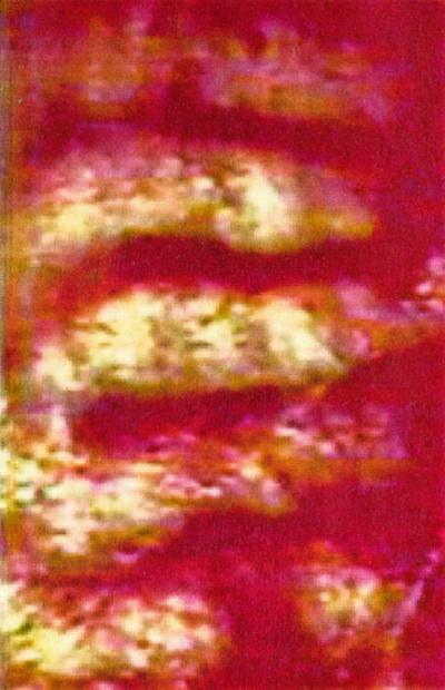
Acoustic wave induced transition to a delocalized state. The pressure wave compresses the array and thereby increases the exchange coupling of the QDs, as discussed in connection with Eq. 1. See ref. 12 for the first experimental report and refs. 13 and 28 for more on the theory. Shown is a videocaptured image of a Langmuir monolayer of 4-nm diameter, pentanethiol passivated Ag QDs that has been compressed, using the mobile barriers of the Langmuir trough, to a point that is just short of the transition from an insulator to a metal. A second Teflon barrier, oriented perpendicular to the principal barriers, was connected mechanically to a speaker, and the speaker was electronically connected to a function generator. A 1-V amplitude, ≈100-Hz square wave function was applied to the speaker and transduced as a mechanical vibration in the second Teflon barrier. The mechanical oscillations corresponded a moving wave of high- and low-pressure oscillations through the monolayer. The silvery components of the monolayer are metallic, whereas the darker, reddish regions are insulating. Other more quantitative measurements have indicated that the metallic regions are, in fact, characterized by a free-electron response in the complex dielectric function—i.e., by a negative valued component of the real part of the dielectric function. This ability to dynamically pattern a macroscopic film as an insulator or a metal is, to our knowledge, unique to these materials.
Figure 2.

A quantum mechanical phase diagram for an array of QDs with size and packing fluctuations. The full phase diagram is actually much richer than what is shown as there are various other ways to tune the relative energies of the system, as discussed in the text.
Disorder has become a parameter that we have been increasingly able to quantify, and so we emphasize the role of disorder by choosing it as the abscissa in the phase diagram. Qualitatively, disorder can arise from size distribution widths and/or packing defects. It is effectively a measurement of the dissimilarity of adjacent dots, and so it acts against a collective behavior. Size fluctuations are obviously coupled to packing disorder but, for a given distribution, one can independently vary the packing disorder via compression of an initially self-assembled lattice. A sufficiently narrow size distribution of QDs will spontaneously crystallize into a well-ordered hexagonal phase (11).
The ordinate in the phase diagram, β, represents the strength of the exchange coupling between adjacent dots. β is large or small in comparison to two other energies. One is the charging energy I, which represents the energetic cost of transferring an electron from one dot to another one that already has its complement of electrons. The exchange coupling β that moves an electron from one dot to another needs to overcome this cost if it is to be effective. The other relevant energy, Δα, is the range of fluctuations in the energy, α, of the exchanged electron. Because the valence electron is confined to the dot, Δα/α is a measure of disorder that arises primarily from the size distribution. β is large if it can bridge the local size fluctuations, β > Δα. By compressing a QD monolayer one can increase β. Because the exchange coupling relies on the overlap of the tails of wave functions that are centered on adjacent dots, β scales exponentially with the distance D between the dots. Thus, through compression, β can be tuned over a wide range. The transition to a collective behavior, when β is sufficiently large, is first order. Our initial observation of an optical signature of this transition (12) could be well reproduced by quantum mechanical computations (13) that allowed for size fluctuations. Since that time we have observed other facets of the phase diagram but much more remains to be done.
The quantitative results on the role of compression for an array of Ag QD could be fitted by using an exchange coupling of the functional form
 |
1 |
R is the radius of the dot, D is the lattice constant, and L is the dimensionless range parameter. For small (2R = 35 Å) Ag dots, 1/2L = 5.5 and β0 = 0.5 eV. The range of strong coupling is determined by the value D0/2R = 1.2 and beyond this point β decreases exponentially. This very same coupling (14) was able to reproduce the experimentally measured effect of lattice compression on the frequency-dependent complex dielectric function (15). In the study of the conductivity (16) reported (see Fig. 5), the dots have twice the radius. Because the exchange coupling depends on the overlap of the wave functions of adjacent dots and so declines exponentially as exp(−κD) where the length scale 1/κ should remain the same, we use 1/2L = 11. Also, to keep the strength of the coupling at contact, D/2R = 1, the same, we use D0/2R = 1.1.
Figure 5.

The temperature dependence of the computed resistivity in the low temperature regime. T in °K for a hexagonal array of 55 dots per side. The plot is for several values of disorder for a compressed lattice, D/2R = 1.21. For lower compressions the resistivity is far higher as it is for more disordered lattices. The logarithmic derivative, dlnR/d  is constant at very low temperatures that shows that lnR scales as
  . T0 ∝ β2/Δα. This means that the charge transfer is not necessarily to the neighboring dot but possibly to a dot that is further away but for which the site energies are more nearly equal. At higher temperatures there is a crossover to an activated transport, ln R ∝ Ea/kT for which case the logarithmic derivative is linear in
  . The value of Ea is not sensitive to the extent of disorder. The resistivity is computed from the transmission that is the thermal average of a weighted density of states for energies above the HOMO (16).
Some disorder is always present, and, even at room temperature, disorder may mask the Mott insulator to metal transition (6) that occurs when the exchange coupling β exceeds the charging energy I. It is easy to assess when this will be the case. Size fluctuations with the resulting variations in the energies of the dots will affect the energy of the ionic bands. When disorder is sufficiently high such that Δα > Ι, the lowest ionic band can overlap the covalent band. This happens when it is energetically advantageous to move an electron from a dot of higher energy α to one with a lower α. The cost is I and the gain is Δα. Indeed, it is even possible for the ionic band to be lowest in energy (17, 18). For highly disordered lattices, the effects of the charging energy therefore will be masked and the key reduced variable is β/Δα.
Even within the limited context of the phase diagram of Fig. 2, the scope of possible transitions is not exhausted by the first-order transition to a collective, delocalized state or the second-order transition between the covalent and ionic states. In the weak coupling regime where β/Δα ≤ 1, the theory suggests that there is another second-order transition, from a localized to a domain localized state (19). In the localized state each electron is defacto confined to a single lattice site; the individual dots are not effectively coupled. It is a strictly insulating state. The domain-localized state has the electrons delocalized over finite QD domains that are smaller than the overall dimensions of the film. This state has recently (19) been imaged by introducing yet another variable, an electric field in the plane of the lattice, and measuring the surface potential (SP) in the x-y plan of the film (20). The domain localized state is not a packing configuration. Fig. 3 shows not only the contours of the SP but also a co-collected topographic image of the QD array, and the images are uncorrelated. Thus, the crystallographic structure of the array can be quite different from the electronic structure.
Figure 3.

SP (Right) and corresponding atomic force microscopy images (Left) of the same silver nanoparticle film, 25 microns in width between the electrodes. The SP images scale from 0.0 V to 0.1 V from dark red to pink, and the topography images scale from 0 nm to 350 nm. Image pairs A–C correspond to a voltage gradient of 0.1, 0.2, and 0.3 V respectively. At 0.4 V, the behavior of the SP image is ohmic-like, showing a monotonic gradation. The structures in the SP images are not correlated to any topographical features. For the film shown D/2R = 1.20 for dots of size = 70 ± 7 Å. The film resistance is 80 MΩ. There is a bright spot near the right electrode, which corresponds to a hole in the conductive film as observed in the topographic image.
Room temperature SP images, collected as the interdot separation distance (D/2R) is decreased, exhibit a transition to a collective behavior. This was seen as an Ohmic-like monotonic drop in the SP across the array. However, consistent with the theory, this delocalization transition was observed only (20) in arrays characterized by a limited amount of disorder. Highly disordered arrays remained domain localized, even at high compression.
Theoretically, we expect that the application of a voltage gradient in the plane of the array will counteract the effects of size disorder. In the presence of an external potential the site energy of the ith dot has the form
 |
2 |
δαi is the fractional range of variation in the site energies, δα, multiplied by a random number between −1 and 1 so that the site energy of the ith dot in the array is α0(1 + δαi). α0Vi is the external potential at the position of the ith dot, computed from the geometry of the array, and e is the charge on the electron. Without an external potential the energies of different dots are uncorrelated. Once a potential is applied, there is a systematic contribution to the site energy. Adjacent dots are correlated if they are oriented in the direction of the potential gradient while they remain uncorrelated otherwise. When the applied gradient is large enough, the systematic monotonic variation in the site energies can compete with the fluctuations. We confirmed this theoretical prediction by increasing the voltage drop per particle. Thereby one can observe (20) a transition from a domain localized state where there are “islands” of higher SP to stripe-like regions where the stripes are directed along the gradient. Such quantum mechanical computational results are shown in ref. 20. Upon further compression the array exhibits a transition to collective behavior, meaning a monotonic drop of the SP in the direction of the applied bias was observed, and also is clearly evident in the computations.
DC transport measurements provide a particularly appealing way to quantify the electronic phase diagram of two-dimensional QD solids in various dimensions, including exchange coupling, temperature, and disorder. Fig. 4 is a representation of the measured resistivity vs. temperature for three different arrays with a small, but finite, size distribution for the dots. Imaging shows these fairly compressed arrays to be regularly ordered in a hexagonal packing. As temperatures drop to about 200 K, such a film will exhibit a decreasing resistance with decreasing temperature, just as any normal metal. At some temperature TMA (180–230 K), the conductivity properties change over to an activated mechanism such that ln(Resistance) ∝ Ea/T. TMA and Ea are linearly correlated, and Ea decreases with increasing lattice compression, implying that these two quantities represent a measurement of the strength of exchange coupling, β. At a lower temperature TAV (20–80 K), the transport characteristics again change, this time to a ln(Resistance) ∝ (T0/T)1/2 dependence. Such a T−1/2 dependence is known in the solid-state theory of amorphous conductors (21) as the regime of variable range hopping (VRH). The transition temperature to VRH, TAV is not correlated with Ea, but it does exhibit a strong, linear dependence on the width of the particle size-distribution. Thus, TAV is a measure of disorder. One interesting prediction that we have extracted from our experiments is that, at size distributions widths <3%, the transition from simple activated to VRH conductivity should disappear. The implication is that the states near the Fermi energy are no longer localized states, but instead are delocalized—such as those that exist at the mobility edge. This observation may have implications for generating true metallic behavior in a two-dimensional lattice down to very low temperatures. Another relevant observation is that the scale parameter T0 for VRH appears to be inversely proportional to the width of the particle size distribution, but there appear to be some scatter in its value for different films. Interestingly, the same is true for the computations discussed below. We understand why that is the case for the computations but we need to further firm up this correspondence, if any, between experiment and theory.
Figure 4.

The temperature dependence of the experimentally determined resistance for 70-Å Ag nanoparticle monolayer films is shown for three different size distributions of particles. All resistance measurements were taken at low bias (−0.3 V to 0.3 V) within the ohmic regime of the I/V curve. Three different temperature regimes are identified. At high temperatures (above ≈200 K) a metallic behavior is seen. Below TMA, the resistance changes over to a simple activated process where ln(Resistance) ∝ Ea/T. TMA is linearly correlated with Ea. At temperatures lower still, below TAV, a ln(Resistance) ∝ (T0/T)1/2 dependence is seen and is interpreted in terms of a variable range hopping mechanism. TAV moves to lower temperatures with decreasing size distribution.
The quantum mechanical computations of the surface potential also can be used to determine the electrical conductivity of the array (16). Such computations assume that the charge transport is coherent. This is analogous to what is done in solid-state physics for so-called mesoscopic systems (22, 23) and for conductivity of molecular wires (24–27). The current is then given by
 |
3 |
Here fl(E) and fr(e) are the Fermi-Dirac occupation probabilities of the left and right electrodes and T(E) is the transmission of the array and is obtained from the scattering computations as the squared modulus of the transition amplitude. In the linear regime one uses a first-order Taylor expansion to bring the voltage V explicitly out. The factor 2 is from the two spin directions. When the voltage drop per site, α0eVi of Eq. 2, is low the computed transmission is independent of the voltage. At higher field gradients the computed transmission function is, by itself, a function of the voltage as discussed in connection with Eq. 2.
The trends in the computed transmission function are those that can be expected from the computations of the SP, as discussed above. In the domain localized regime the transmission is negligible unless the external voltage is high enough that stripes can be formed. Upon compression, the transmission increases exponentially up to where the dot-dot exchange coupling β saturates, as in Eq. 1. This saturation is as we have previously seen for both experiment and computations of the second harmonic response. On the other hand, the transmission function depends on the energy and this dependence is nontrivial even in the strong coupling regime (16).
Low temperature measurements of the conductivity probe the energy dependence of the transmission on a very fine scale. The simple Hamiltonian that we use for computing and interpreting the other response functions of QD arrays does predict the observed trends in the conductivity (Fig. 5). We turn to a brief interpretation of the computational results. The key point is that, in the mesoscopic regime, the transmission is a weighted density of states. The implication is that the transmission has a cusp-like gap at the Fermi surface. (The detailed shape of the gap depends on the role of the charging energy I and its magnitude as compared to the range Δα of the fluctuation in site energies.) This gap is being filled in as the disorder is increasing so that, at a high enough disorder the gap disappears. Similarly, the gap disappears as the lattice is expanded so that β decreases. We attribute the lower temperature behavior to the contribution of states in the gap in the transmission that is made possible by thermal excitation. Once the temperature is somewhat higher, one can access energies above the gap and the behavior changes over to a regular activated regime. Another factor that is relevant to the crossover is the exact position of the gap. At the highest possible values of β, that is, at a tightly compressed hexagonal lattice, the highest occupied level in the ground state (the HOMO in chemical terminology or the Fermi energy of solid state) is somewhat above the gap. Then, as the lattice is expanded, the energy of the highest orbital shifts down with respect to the gap and the role of the gap is more evident in the temperature dependence of the conductivity. It is an open question whether this effect, as seen in the computations, has an experimental counterpart. A final caveat about the computation is the sampling of disorder. We have computed by using hexagonal arrays of 55 dots per side, 8,911 dots in all. Even for such large arrays, there are few enough disorder-induced states in the gap that the scale parameter T0 is not strictly independent of the specific distribution of dot energies. Invariably, T0 scales as β2/Δα where Δα is a measure of the variance of the site energies. The magnitude of T0 (below 0.5 eV) is in the same range as was observed, but it is somewhat sensitive to higher moments of the size distribution. This is not unexpected because the theory of domain localized regime (19) tells us that variable range coupling should scale with the variance of β2/α (which is not the same as β2/variance of α). Finally we mention that starting from the transmission function vs. energy, the resistivity as shown in Fig. 5 is not computed numerically but analytically and this makes it a rather sensitive probe for the role of temperature. In particular, the logarithmic derivative of the resistivity with respect temperature can be analytically computed.
In conclusion, temperature provided us with a finer probe of transport in QD arrays and highlighted effects of disorder not hitherto observed.
Acknowledgments
This work was funded by the Department of Energy and a Collaborative University of California/Los Alamos Research grant. F.R. is a “Maître de Recherches,” Fonds National de la Recherche Scientifique, Belgium and thanks Liège University for a “Crédit d'impulsion” grant. Computational facilities were provided by Sonderforschunbereich 377 (Hebrew University) and Numerically Intensive Computing (Liège University).
Abbreviations
- QD
quantum dot
- SP
surface potential
Footnotes
This paper results from the Arthur M. Sackler Colloquium of the National Academy of Sciences, “Nanoscience: Underlying Physical Concepts and Phenomena,” held May 18–20, 2001, at the National Academy of Sciences in Washington, DC.
References
- 1.Markovich G, Collier C P, Henrichs S E, Remacle F, Levine R D, Heath J R. Acc Chem Res. 1999;32:415–423. [Google Scholar]
- 2.Schon J H, Kloc C, Hwang H Y, Batlogg B. Science. 2001;292:252–254. doi: 10.1126/science.1058812. [DOI] [PubMed] [Google Scholar]
- 3.Mannhart J. Philos Trans R Soc A. 1995;353:377–385. [Google Scholar]
- 4.Lin X M, Jaeger H M, Sorensen C M, Klabunde K J. J Phys Chem B. 2001;105:3353–3357. [Google Scholar]
- 5.Peng Z A, Peng X G. J Am Chem Soc. 2001;123:183–184. doi: 10.1021/ja003633m. [DOI] [PubMed] [Google Scholar]
- 6.Mott N F. Metal-Insulator Transitions. London: Taylor & Francis; 1990. [Google Scholar]
- 7.Kubo R. J Phys Soc Japan. 1962;17:975–986. [Google Scholar]
- 8.Lambe J, Jaklevic R C. Phys Rev Lett. 1969;22:1371–1375. [Google Scholar]
- 9.Murray C B, Kagan C R, Bawendi M G. Annu Rev Mat Sci. 2000;30:545–610. [Google Scholar]
- 10.Puntes V F, Krishnan K M, Alivisatos A P. Science. 2001;291:2115–2117. doi: 10.1126/science.1057553. [DOI] [PubMed] [Google Scholar]
- 11.Heath J R, Knobler C M, Leff D V. J Phys Chem. 1997;101:189–197. [Google Scholar]
- 12.Collier C P, Saykally R J, Shiang J J, Henrichs S E, Heath J R. Science. 1997;277:1978–1981. [Google Scholar]
- 13.Remacle F, Collier C P, Heath J R, Levine R D. Chem Phys Lett. 1998;291:453–458. [Google Scholar]
- 14.Remacle F, Levine R D. J Am Chem Soc. 2000;122:4084–4091. [Google Scholar]
- 15.Henrichs S, Collier C P, Saykally R J, Shen Y R, Heath J R. J Am Chem Soc. 2000;122:4077–4083. [Google Scholar]
- 16. Remacle, F., Beverly, K. C., Heath, J. R. & Levine, R. D. (2002) J. Phys. Chem., in press.
- 17.Kim S H, Medeiros-Ribeiro G, Ohlberg D A A, Williams R S, Heath J R. J Phys Chem B. 1999;103:10341–10347. [Google Scholar]
- 18.Remacle F, Levine R D. J Phys Chem A. 2000;104:10435–10441. [Google Scholar]
- 19.Remacle F, Levine R D. J Phys Chem B. 2001;105:2153–2162. [Google Scholar]
- 20.Sample J L, Beverly K C, Chaudhari P R, Remacle F, Heath J R, Levine R D. Adv Mat. 2001;14:124–128. [Google Scholar]
- 21.Shklovskii B I, Efros A L. Electronic Properties of Doped Semiconductors. Berlin: Springer; 1984. [Google Scholar]
- 22.Datta S. Electronic Transport in Mesoscopic Systems. Cambridge, U.K.: Cambridge Univ. Press; 1995. [Google Scholar]
- 23.Imry Y, Landauer R. Rev Mod Phys. 1999;71:S306–S312. [Google Scholar]
- 24.Mujica V, Kemp M, Ratner M A. J Chem Phys. 1994;101:6849–6855. [Google Scholar]
- 25.Yaliraki S N, Ratner M A. J Chem Phys. 1998;109:5036–5043. [Google Scholar]
- 26.Samanta M P, Tian W, Datta S, Henderson J I, Kubiak C P. Phys Rev B. 1996;53:R7626–R7629. doi: 10.1103/physrevb.53.r7626. [DOI] [PubMed] [Google Scholar]
- 27.Tian W D, Datta S, Hong S H, Reifenberger R, Henderson J I, Kubiak C P. J Chem Phys. 1998;109:2874–2882. [Google Scholar]
- 28.Remacle F, Levine R D. Proc Natl Acad Sci USA. 2000;97:553–558. doi: 10.1073/pnas.97.2.553. [DOI] [PMC free article] [PubMed] [Google Scholar]