

Abstract
The fabrication and characterization of tungsten nanoelectrodes insulated with cathodic electrophoretic paint is described together with their application within the field of neurophysiology. The tip of a 127 μm diameter tungsten wire was etched down to less than 100 nm and then insulated with cathodic electrophoretic paint. Focused ion beam (FIB) polishing was employed to remove the insulation at the electrode’s apex, leaving a nanoscale sized conductive tip of 100–1000 nm. The nanoelectrodes were examined by scanning electron microscopy (SEM) and their electrochemical properties characterized by steady state linear sweep voltammetry. Electrode impedance at 1 kHz was measured too. The ability of a 700 nm tipped electrode to record well-isolated action potentials extracellularly from single visual neurons in vivo was demonstrated. Such electrodes have the potential to open new populations of neurons to study.
1. Introduction
The use of insulated metal microelectrodes in the field of neurophysiology dates back many decades (e.g. Kuffler 1953, Hubel 1959) and today the same probes with minor modification continue to provide neurophysiologists with useful information about the functioning of neurons. More recently, similar probes have been used in the field of electroanalytical chemistry (Ewing et al 1981, Fleischmann and Pons 1987) and, as analytical chemists have sought greater resolution, they have come to develop electrodes with smaller tips than those routinely employed by neurophysiologists (reviewed by Zoski 2002, Arrigan 2004). Hence, leadership in the hunt to produce small tipped electrodes has shifted from the field of neurophysiology to the field of analytical chemistry. Herein we redress that balance slightly by describing the fabrication of a new nanoelectrode that is designed for neurophysiology.
It has long been appreciated by neurophysiologists that sampling of neurons is biased by the size of the tip of the electrode used in neurophysiological recordings (Towe and Harding 1970, Stone 1973). Many populations of neurons remain understudied because they are small and their signals rarely recorded with currently available electrodes. We believed therefore that there could be an advantage to developing nanoscale tipped electrodes for neurophysiology. Perhaps signals from these small neurons that were difficult or near impossible to record with the standard electrodes neurophysiologists use would become accessible with smaller tipped electrodes. Below we report a method for reliably fabricating nanoscale tipped electrodes and provide evidence that they can record action potentials from neurons with good signal-to-noise ratio. Since some of our method for fabrication is novel, electroanalytical chemists might also be interested in following our approach.
A variety of techniques have been used to fabricate nanometre scale electrodes for applications such as liquid scanning tunnelling microscopy (STM) and scanning electrochemical microscopy (SECM) (e.g. Gewirth et al 1989, Slevin et al 1999). A common approach has been to etch a metal wire electrochemically to produce a nanoscale diameter tip and then coat the wire with an insulating material sparing the apex. A number of coating methods have been reported, such as translating the wire through molten paraffin (Zhang and Wang 1994), dipping the wire into varnish (Gewirth et al 1989) or apiezon wax (Nagahara et al 1989). However, these methods produce electrodes with inconsistent geometry and dimensions and often with pinholes on the shank of the electrode. While the latter might not pose a problem for scanning electrochemical studies, it is a concern for neurophysiologists because their electrodes must often travel through centimetres of brain tissue and it is not generally desirable to pick up signals from multiple sites along the electrode.
Recently, cathodic electrophoretic paint has been employed to insulate electrodes (Slevin et al 1999, Chen and Kucernak 2002). Electrophoretic paint was developed by the Ford Motor Company in the 1950s as a protective coating for car bodies and has been used widely for this purpose since the 1970s. In the early 1990s scientists exploited it as an insulator for STM tips (Mao et al 1992, Bach et al 1993). Its advantage stems mainly from the robust coat it provides and the convenient method of application. Cathodic electrophoretic paint can be coated onto metal wires by electrodeposition and heat cured to provide good insulation. During heat curing, the cathodic electrophoretic paint shrinks, leaving a conductive apex exposed. Unfortunately, it is hard to control the curing process to give a conductive tip with consistent dimensions and geometry. Also the curing process, which is intended to make only the apex conductive, often leaves pinholes on the electrode body. It is hard therefore to ensure that there are no conductive pinholes on the body of the electrode while leaving the apex conductive. The above disadvantages make this heat curing approach inefficient for the fabrication of probes for neurophysiology. In our experience, several coats of paint are needed to eliminate pinholes from the body of the electrode, which adds to the difficulty in accomplishing an electrode with a conductive tip. The production rate of good electrodes through the heat curing method is low (no better than an ~20% success rate).
In this paper, we report a procedure for fabricating tungsten nanoelectrodes of consistent tip dimension with high efficiency. Etched tungsten wire is coated and cured through several cycles to ensure the whole electrode is insulated. Then a focused ion beam (FIB) is employed to polish away the paint insulation from the tip. The conductive apex area and its geometry are well controlled and an almost 100% rate of successful production is achieved. The electrodes have been characterized by scanning electron microscopy (SEM), steady state linear sweep voltammetry and by impedance at 1 kHz. The use of these electrodes in neurophysiology is demonstrated by their ability to obtain in vivo extracellular recordings of action potentials from single cat neurons.
2. Methods and experimental results
2.1. Chemicals and solutions
Cathodic electrophoretic paint HSR was supplied by Clearclad (USA). Potassium ferrocyanide was purchased from Aldrich. Sodium nitrate, potassium hydroxide and glacial acetic acid were purchased from Fisher Chemicals. All aqueous solutions were prepared with distilled water that was purified further via a Barnstead E-Pure system.
2.2. Fabrication of tungsten nanoelectrode
Tungsten wire (127 μm diameter and ~10 cm length, Small Parts, USA) was cleaned with acetone followed by distilled water. The tungsten wire was etched by the following procedure, slightly modified from Levick (1972). 4 V DC was set up between the tungsten wire (anode) and a graphite counter-electrode (cathode). The etching solution consisted of 10 mol dm−3 sodium nitrite and 6 mol dm−3 potassium hydroxide. In order to generate a cone-shaped tip, the wire was repeatedly dipped in and out of the etching solution to a maximum immersion depth of 3 mm. The dipping motion was controlled by a sewing machine adapted for this purpose. During the etching process, gas evolves from the interface between the tungsten and the etching solution. It takes roughly 4 min to etch a cone-shaped nanoscale sized tip, but many pieces of tungsten can be etched simultaneously. Figure 1(a) shows an SEM image of a tungsten electrode etched by this method with an apex diameter of ~100 nm. A LEO 1525 SEM was used to image this and all the other samples shown in this paper.
Figure 1.
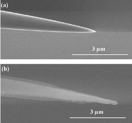
(a) SEM image of an electrochemically etched tungsten wire. (b) SEM image of etched tungsten coated with cathodic electrophoretic paint, which shows as a semi-transparent layer.
Insulation of the etched tungsten electrode was achieved through electrodeposition of cathodic electrophoretic paint. To ensure uniform coating, the etched tungsten was cleaned with dilute hydrofluoric acid (<1%) to remove its natural oxide layer, and then rinsed with distilled water. The Clearclad HSR cathodic electrophoretic paint solution was mixed with glacial acetic acid with a ratio of ten parts of paint to one part of acetic acid. Then the etched tungsten electrode (cathode) and a graphite rod (anode) were immersed into this paint solution. 20 V DC between the tungsten electrode and the graphite rod for 120 s was found to provide a uniform coat. Excess paint was washed away with distilled water. The coated tungsten was then baked in a furnace at 205 °C for 20 min. The coating and baking procedures were repeated several times to ensure complete insulation. The quality of insulation was checked by linear sweep voltammetry using the coated tungsten as the working electrode. In most cases, three cycles of coating and baking reduced the leakage current to less than 0.1 nA. Figure 1(b) shows the SEM image of a tungsten electrode after three cycles of coating and baking. A high acceleration voltage (30 kV), short working distance (~5 mm) and secondary-electron detector were used to obtain this image. Because cathodic electrophoretic paint mainly consists of the elements C and H, which scatter electrons less effectively than tungsten, the high energy electrons can penetrate the thin paint layer and render this layer semi-transparent. Hence, these working parameters for the SEM enabled us to discriminate the cathodic electrophoretic paint layer from the tungsten.
The final step was to remove the insulation from the apex of the tungsten electrode. This was accomplished by ion beam polishing with a Hitachi FIB 2000A, with a liquid gallium metal source used for machining. A dozen coated tungsten electrodes were mounted by carbon tape on a silicon substrate and then placed inside the FIB chamber. First an image was formed of the electrodes with low beam current (<1 pA) and low acceleration voltage (3 kV). The ion beam was then focused on the tapered ends of the electrodes and the beam current increased to 1 nA and the acceleration voltage increased to 30 kV. The insulating layer of paint at the electrode tips was polished away at a considerable speed while the polishing process itself was observed. After polishing the upper side of the electrode tips, the electrodes mounted on the silicon substrate were removed and flipped over to permit polishing of the other side. It takes 1 h to make a dozen nanoelectrodes with a 100% success rate. The geometry and area of the exposed tungsten tip depends on how large an area of the tip the ion beam is focused onto, which is limited only by the resolution of the FIB system (~10 nm). Figure 2 shows SEM images of tungsten micro- and nanoelectrodes fabricated by this technique.
Figure 2.
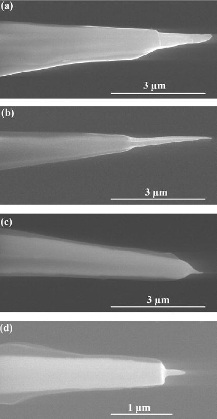
(a)–(d) SEM images of cathodic electrophoretic paint insulated tungsten micro- and nanoelectrodes.
2.3. Linear sweep voltammetry
Linear sweep voltammetry was used to determine the electroactive area of the tungsten nanoelectrodes. A CHI 1202 electrochemical analyser was used to perform the linear sweep voltammetry, in which the tungsten nanoelectrode served as the working electrode. The counter-electrode was platinum and the reference electrode was Ag/AgCl/KCl (sat.). The electrolyte was 1.0 × 10⁻² mol dm−3 K4Fe(CN)6 with a supporting electrolyte of 2.0 mol dm−3 KCl. Voltage was scanned from −0.2 to 1.1 V with a scan rate of 0.05 V s−1. Figure 3 shows the steady state voltammograms for the oxidation of Fe(CN)4−6 using the tungsten electrodes shown in figure 2. By measuring the linear steady state diffusion limited current, and by approximating the apex geometry of the electrode as a hemisphere (Penner et al 1989, 1990), the effective radius of the tungsten tips can be calculated from equation (1):
Figure 3.
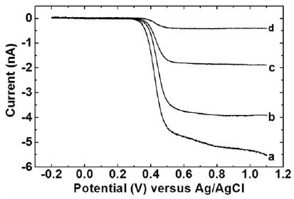
Linear sweep voltammograms for the oxidation of 1.0 × 10⁻² mol dm−3 Fe(CN)64− in supporting electrolyte of 2.0 mol dm−3 KCl using the tungsten electrodes shown in figure 2. Lines labelled with (a), (b), (c) and (d) correspond to the tungsten electrodes shown in figure 2 as (a), (b), (c) and (d), respectively. The effective radii of these electrodes were fitted with equation (1) and found to be (a) 1.3 μm (b) 1 μm (c) 450 nm and (d) 100 nm.
| (1) |
where D and C are the diffusion coefficient and concentration of the electroactive species in the electrolyte, n is the number of electrons transferred during each oxidation, and F is the Faraday constant. In our case, D is 6.7 × 10⁻⁶ cm2 s−1 and n equals 1. The hemisphere approximation gives a rough estimate of tip radius, which can be compared against the apex sizes estimated from their SEM images. For the cases shown in figure 3, the effective radii were calculated to be 1.3 μm (a), 1 μm (b), 450 nm (c), and 100 nm (d), respectively. These electrochemically calculated apex radii were in close agreement with the SEM observations.
2.4. Impedance measurements
The impedance at 1 kHz of electrodes used for extracellular neurophysiology is commonly taken as a measure of tip size; the frequency 1 kHz being chosen because these electrodes are intended to record action potentials that are ~1 ms in duration. The 1 kHz impedances of seven electrodes with tips ranging from 400 nm to 2 μm were measured with a Solartron 1260 impedance/gain-phase analyser. Impedance was measured with the tips submerged ~2 mm into physiological saline for a 1 kHz 10 nA amplitude current. Figure 4 plots impedance versus tip size. As one would expect, impedance grows as tip size gets smaller. Interestingly, the log–log slope of the relationship is very close to −1.
Figure 4.
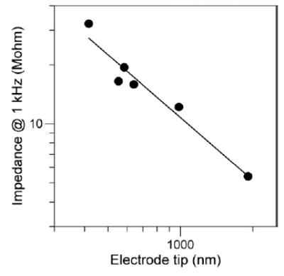
Electrode impedance at 1 kHz versus tip size on double-logarithmic axes. The regression line has a slope of −1 indicating that impedance is hyperbolically related to tip length in this case.
2.5. In vivo extra cellular recording
Electrodes fabricated by the procedure described above were tested and found to record action potentials extracellularly from single neurons in the in vivo cat. Results for one electrode with an effective radius ~700 nm are shown for the purpose of demonstration. This electrode was inserted into the cat’s brain through a guide tube made from a 22G needle. Electrical signals were recorded with the electrode, amplified by an EX-1000 10 channel extracellular amplifier (Dagan Corporation, Minnesota), and displayed on an oscilloscope screen. During the experiment, the electrode picked up many spikes (action potentials) while descending through the cat brain. We found that it could record well-isolated action potentials from single neurons for more than 50 min, a recording time sufficient for many neurophysiological studies. Figure 5 shows action potentials recorded from single optic tract fibres. In both cases shown the recordings were from axons of X-cells. Similar and often even better signal-to-noise ratio recordings were obtained with the larger caliber Y-cell axons (Enroth-Cugell and Robson 1966). Although one necessarily encounters spikes of smaller amplitude, those whose amplitudes are ~4 times the noise amplitude or greater generally provide more stable recordings. We encountered many cells whose discharges met this criterion on each penetration. X-cells typically had signal amplitudes 4–8 times the noise amplitude and Y-cells with signal amplitudes 10 times or greater than the noise.
Figure 5.

Traces showing action potentials recorded from two optic tract fibres of the cat with a paint insulated tungsten nanoelectrode. Note the excellent signal-to-noise discrimination. Both recordings are from X-cell axons.
The optic tract lies at a depth of ~2 cm below the cat’s brain surface. The average diameters of X- and Y-cell axons, excluding their myelin coats, are ~2.5 μm and ~5 μm, respectively (Williams and Chalupa 1983). The small size of the axons, particularly the X-cell axons, together with the dense packing of optic tract fibres means that fine electrodes are needed firstly to record and secondly to isolate the signals of an individual axon from those nearby. The fact that excellent extracellular recordings were made from small neural processes indicates that electrodes with tips smaller than 1 μm can be useful to neurophysiologists. We believe that this is the first report of successful extracellular neurophysiological recordings with nanoscale metal tipped electrodes. That recordings were achieved from a deep structure is especially impressive, demonstrating the durability of the electrodes in penetrating far into brain tissue. Further evidence of the electrodes’ durability is that they could be used for multiple penetrations through the cat brain (on average ~3 tracts), with recordings of the quality shown in figure 5 obtained in each case. So far our experience has been that the nanoelectrodes are at least as durable as the larger (5–10 μm) tipped tungsten-in-glass Levick-style (1972) microelectrodes that we have used for optic tract recordings from cats for more than 15 years.
3. Summary
We have demonstrated a method for fabricating cathodic electrophoretic paint coated tungsten nanoelectrodes by focused ion beam milling. Unlike the case for previously reported methods of making electrodes, our method has a 100% success rate and the tip geometry and size can be very well controlled. Furthermore, our method can ensure that the only conductive area of the electrode is its tip and that there are no pinholes on the electrode body. The fabricated nanoelectrodes have been characterized by SEM, linear sweep voltammetry and for impedance at 1 kHz. Successful application of fabricated tungsten nanoelectrodes for extracellular recording from single visual neurons of a living cat has been demonstrated.
Acknowledgments
This work was supported by grants from Northwestern University’s Institute for Bioengineering and Nanoscience in Advanced Medicine, by NIH grants R01 EY06669 and R21 EB004200, and from the NASA University Research, Engineering and Technology Institute on Bio Inspired Materials (BIMat) under award No. NCC-1-02037.
References
- Arrigan DWM. Analyst. 2004;129:1157–65. doi: 10.1039/b415395m. [DOI] [PubMed] [Google Scholar]
- Bach CE, Nichols RJ, Beckmann W, Meyer H, Schultze A, Besenhard O, Jannakoudakis PD. J Electrochem Soc. 1993;140:1281–4. [Google Scholar]
- Chen S, Kucernak A. Electrochem Commun. 2002;4:80–5. [Google Scholar]
- Ewing AG, Dayton MA, Wightman RM. Anal Chem. 1981;53:1842–7. [Google Scholar]
- Fleischmann M, Pons S. Anal Chem. 1987;59:1391A. [Google Scholar]
- Enroth-Cugell C, Robson JG. J Physiol. 1966;187:517–52. doi: 10.1113/jphysiol.1966.sp008107. [DOI] [PMC free article] [PubMed] [Google Scholar]
- Gewirth AA, Craston DH, Bard AJ. J Electroanal Chem. 1989;261:477–82. [Google Scholar]
- Hubel DH. J Physiol. 1959;147:226–38. doi: 10.1113/jphysiol.1959.sp006238. [DOI] [PMC free article] [PubMed] [Google Scholar]
- Kuffler SW. J Neurophysiol. 1953;16:37–68. doi: 10.1152/jn.1953.16.1.37. [DOI] [PubMed] [Google Scholar]
- Levick WR. Med Biol Eng. 1972;10:510–5. doi: 10.1007/BF02474199. [DOI] [PubMed] [Google Scholar]
- Mao BW, Ye JH, Zhou XD, Mu JQ, Fen ZD, Tian ZW. Ultramicroscopy. 1992;42–44:464–7. [Google Scholar]
- Nagahara LA, Thundat T, Lindsay SM. Rev Sci Instrum. 1989;60:3128–30. [Google Scholar]
- Penner RM, Heben MJ, Lewis NS. Anal Chem. 1989;61:1630–6. [Google Scholar]
- Penner RM, Heben MJ, Longin TL, Lewis NS. Science. 1990;250:1118–21. doi: 10.1126/science.250.4984.1118. [DOI] [PubMed] [Google Scholar]
- Slevin CJ, Gray NJ, Macpherson JV, Webb MA, Unwin PR. Electrochem Commun. 1999;1:282–8. [Google Scholar]
- Stone J. J Neurophysiol. 1973;36:1071–9. doi: 10.1152/jn.1973.36.6.1071. [DOI] [PubMed] [Google Scholar]
- Towe AL, Harding G. Exp Neurol. 1970;29:366–81. doi: 10.1016/0014-4886(70)90065-8. [DOI] [PubMed] [Google Scholar]
- Williams RW, Chalupa LM. J Neurosci. 1983;3:1554–64. doi: 10.1523/JNEUROSCI.03-08-01554.1983. [DOI] [PMC free article] [PubMed] [Google Scholar]
- Zhang B, Wang E. Electrochim Acta. 1994;39:103–6. [Google Scholar]
- Zoski CG. Electroanalysis. 2002;14:1041–51. [Google Scholar]