Abstract
Microelectronic-based biosensors that allow noninvasive measurement of cell activity are in the focus of current developments, however, the mechanisms underlying the cell-transistor coupling are not completely understood. In particular, characteristic properties of the extracellular voltage response such as the waveform and amplitude are not satisfactorily described by electrical circuit models. Here we examine the electrical coupling between a nonmetallized field-effect transistor (FET) and a cell line expressing a voltage-gated EAG K+ channel. The activation kinetics of this channel depends on the voltage pulse protocol and extracellular divalent cations. This feature allows testing, whether the extracellular voltage signal recorded with the FET faithfully tracks the current simultaneously recorded with the patch-clamp technique. We find that the FET signals contain different kinetic components that cannot be entirely explained by equivalent electrical-circuit models. Rather, we suggest that changes in ion concentration in the small cleft between cell and FET may change the surface potential of the FET. This study provides evidence that the electrochemical processes at the cell-transistor interface are complex and that at least two different mechanisms contribute to the shape and amplitude of transistor signals.
INTRODUCTION
The extracellular recording of cellular activity provides a powerful, noninvasive technique that holds great promise for biomedical studies. In contrast to classical electrophysiological methods, silicon devices allow stable long-term recordings of electrical activity from single cells or networks of cells cultured on planar surfaces. Signals from neurons or other electrically active cells have been recorded using microelectrode arrays of metallized electrodes on glass or silicon substrates (1) or nonmetallized field-effect transistors (FET) (2,3). Such devices have also been used to stimulate neurons electrically (4–6).
The “open gate” of a FET can register the electrical activity of cells attached to the gate region (2,7). Changes in the drain-source current of the FET are correlated with voltage changes in the small cleft between cell and transistor surface (8,9). The extracellular voltage signals have been interpreted in terms of equivalent electrical-circuit models. For example, the point-contact model describes the electrical coupling between a cell and a transistor gate by a single point of contact (10). The model has been further developed to incorporate a two-dimensional contact area (11). Subsequently, properties of the cell membrane have been incorporated, such as the specific membrane conductance and the surface area of the membrane-transistor contact (9,12). Despite these improvements, the models do not adequately describe several aspects of the extracellular signals. For example, the amplitude and the time course of the FET signals produced by A-type and K-type potassium currents in hippocampal neurons are not adequately predicted (13). The initial current transient that is mediated by rapidly inactivating A-type K+ channels was missing in the transistor signal. Moreover, the transistor signals that were recorded during activation of K-type K+ channels were significantly larger than predicted by the simulation. To account for these discrepancies, it has been proposed that K-type K+ channels are enriched, whereas A-type K+ channels are depleted from the contact area (13,14). Accumulation of channels has also been proposed for maxi K+ channels expressed in HEK 293 cells (14).
To advance our understanding of the nature of the FET signals, we coupled HEK 293 cells that expressed a voltage-gated K+ channel to n- and p-channel FETs. The ion channel belongs to the family of ether-á-gogo (EAG) channels. The kinetics of EAG channel activation strongly depends on the voltage-step protocol and the presence of extracellular divalent cations, for example Mg2+ and Co2+ (15–18). Thereby, this cell system provides a unique opportunity to modulate the kinetics and shape of whole-cell membrane currents and to compare it with the recorded FET signals.
We find that, for fast EAG channel activation, the increase of the FET signal is slower than the time course of the whole-cell current. Moreover, when the whole-cell current rapidly turned off by repolarization, the FET signal declines with two kinetic components: a fast component that follows the whole-cell current and a slow component that seems to be unrelated to the whole-cell current. The slow component differs strongly in amplitude between p- and n-channel FETs and cannot be explained by the redistribution of ion channels.
MATERIALS AND METHODS
Field effect transistor chips
The p-channel FET devices used for the extracellular recordings were first described by Offenhäusser et al. (19). Here we used an improved version: a second implantation step for drain-source doping reduced the series resistance of the contact lanes and, thereby, decreased the noise level of the p-channel transistor (20). In addition, we used n-channel transistors with a lower noise level that were fabricated according to Krause (20). A shallow implant through a 220-nm SiO2 layer in the gate area buried the n-channel; this procedure lowered the 1/f noise (21).
Both types of FETs consisted of 16 transistor gates arranged in a 4 × 4 matrix (100 or 200 μm pitch) in the center of a 5 × 5 mm2 silicon chip. Gate oxide was fabricated by thermal oxidation of silicon (8-, 10-, or 12-nm thickness). The gate oxide area exposed to the electrolyte solution was 5 × 8 μm2, 6 × 8 μm2, or 7 × 8 μm2. Effective gate length of the FETs was 1–2 μm. The transconductances were gm = 0.2–0.6 mS for the p-channel and 0.5–1.4 mS for the n-channel devices, depending on the thickness of the gate oxide and the gate dimensions. The root mean-square noise was ∼100 μV for p-channel and ∼45 μV for n-channel transistors. The surface of the chips was passivated by an ONO layer (SiO2 / Si3N4 / SiO2), which allowed multiple reuses of the chip. Details of the fabrication, the encapsulation process, and the amplifier systems have been described elsewhere (19,22,23).
The FET setup used in this study has been previously described (22). In the working point, a constant working current of the FET of 0.1–1 mA (depending on the FET design) superimposed the recorded changes of drain-source current IDS. The FET amplifier system used a feedback circuitry, which subtracted the output signal from the baseline and compensated the constant dc-offset (24).
The working point of the FETs was determined by measuring the transfer characteristics IDS (VGS). The p-channel FETs were biased with drain-source voltages VDS and gate-source voltages VGS from 0 to −3 V, and the n-channel FETs with voltages from 0 to +3 V. An extracellular Ag/AgCl electrode, which was set to ground potential, served as reference electrode for both the gate contact of the FETs and the patch-clamp recordings. Thus, the source and the bulk of the FETs had to be set to a positive voltage to result in negative VGS for the p-channel FETs and to a negative voltage to result in positive VGS for the n-channel FETs.
The K+ ion sensitivity of the FETs (SFET) has been studied with solutions of from 0.1 mM to 1 M KCl (10 mM HEPES, pH 7.4, adjusted with TRIS) with constant ionic strength of 2 M (adjusted with CaCl2). We found a nonlinear relationship for the response of p-channel FETs: 0.7 ± 0.5 mV/pK for K+ concentrations  and 3.8 ± 1.7 mV/pK for
  These values were smaller compared to those reported in literature: 6–8 mV/pK (for
  ) up to 10–15 mV/pK (for
  ) (25).
Chip cleaning and surface modification
The chip surface was cleaned twice by ultrasonification for 5 min in 2% (v/v) Hellmanex II (Hellma, Müllheim, Germany) and bidistilled water. The surface was further treated by incubation in 20% (v/v) H2SO4 for 20 min at 80°C. The chips were rinsed with bi-distilled water and kept for 5 min in 99.8% (v/v) ethanol. After rinsing two times with PBS buffer (137 mM NaCl, 2.7 mM KCl, 8.1 mM Na2HPO4, 1.5 mM KH2PO4, pH 7.3), FET surfaces were coated for 30 min with 25 μl of 0.1 mg/ml poly(l)lysine (Sigma, Taufkirchen, Germany) at room temperature. The surfaces were rinsed with PBS before plating the cells.
HEK 293 cells expressing EAG channels
The beag1 gene (16) was subcloned from a pcDNA1.1 construct into the BamHI and XbaI restriction sites of a pcDNA3.1 vector (Invitrogen, Breda, The Netherlands) by standard cloning techniques. Approximately 10 μg of the recombinant plasmid DNA were introduced into exponentially growing HEK 293 cells (∼2 × 10⁵ cells per 50-mm dish) by a modified calcium phosphate method (26). Cells were grown in minimal essential medium (M2279, Sigma) supplemented with 2 mM glutamine, nonessential amino acids, 10% (v/v) fetal calf serum, 100 units/ml penicillin, and 0.1 mg/ml streptomycin (M10 medium). Transformed clones were selected in the presence of 1.0 mg/ml of the antibiotic G418 (Sigma). Isolated foci were propagated in M10 medium with 0.8 mg/ml G418. Expression of EAG channels was determined by electrophysiological recordings.
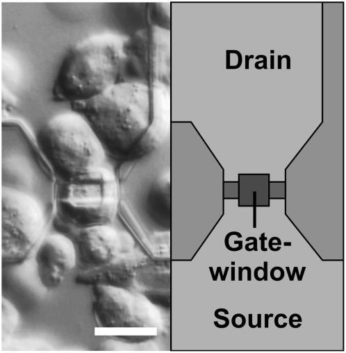
Cells were cultured in 50-mm dishes and split weekly. For plating onto the FET chips, the cells were trypsinized for 5 min at 37°C (0.5 mg/ml trypsin; 0.2 mg/ml EDTA, Sigma). Detached cells were suspended in M10 medium and centrifuged for 5 min at 200 × g. Cells were plated onto the poly(l)lysine-coated FETs at densities of 4500–6000 cells per chip (effective chip surface, 6.2 mm2). The chips were kept at 37°C and 5% CO2 for 3–5 days in a humidified chamber. Fig. 1 shows a microscope image of HEK 293 cells grown for 4 days on a gate structure.
FIGURE 1.
Differential interference contrast micrograph of HEK 293 cells on a poly(l)lysine-coated chip surface after 4 days in culture (left) and a schematic drawing of the FET (right). The gate of the transistor (width, 8 μm; length, 5 μm) inside the gate window is connected to the drain (top) and the common source (bottom). Scale bar = 20 μm.
Electrophysiology
After 3–5 days in culture, membrane currents were recorded by the patch-clamp technique in the whole-cell configuration (27) with an EPC-9 patch-clamp amplifier (HEKA Elektronik, Lambrecht, Germany). Changes of IDS of the transistor located below the patch-clamped cell were amplified and fed into the external input of the EPC-9 patch-clamp amplifier.
Membrane current signals and corresponding FET signals were recorded simultaneously at 12 kHz and averaged using the TIDA software (HEKA Elektronik). Patch pipettes (3.8–5.2 MΩ) were filled with intracellular solution (125 mM KCl, 2 mM MgCl2, 10 mM EGTA-KOH, 10 mM HEPES, 5 mM Na-ATP, adjusted to pH 7.4 with KOH). The extracellular solution was 5 mM KCl, 140 mM NaCl, 10 mM HEPES, 5 mM glucose, adjusted to pH 7.4 with NaOH. By adding different divalent cations we obtained extracellular Ca2+ solution (1 mM CaCl2), extracellular Ca2+/Mg2+ solution (5 mM MgCl2, 1 mM CaCl2), and extracellular Ca2+/Co2+ solution (2 mM CoCl2, 1 mM CaCl2). In the following, these solutions will be referred to as Ca2+-, Mg2+-, and Co2+ solutions. The presence of Ca2+ in all solutions was required for sufficient patch stability. The membrane capacitance of the cells (n = 52) was CM = 15.4 ± 4.0 pF, the membrane resistance was RM = 2.8 ± 1.7 GΩ, and the series resistance of the cell-pipette contact was RS = 10.9 ± 4.9 MΩ. The values of CM and RS were compensated by the EPC-9 amplifier using the TIDA software (28,29).
Recordings from cells that only partially covered the transistor gate showed smaller amplitudes, leading to a significantly lower signal/noise (S/N) ratio. Therefore, we describe only signals recorded from cells completely covering the FET gates.
RESULTS
Extracellular recordings with a p-channel FET
We chose a cell line expressing EAG channels to study the nature of the contact at the cell-transistor interface. The activation kinetics of the channel can be manipulated by various means. Therefore, this channel is suitable to test, whether the changes in the gate voltage of the FET (VFET) faithfully recapitulate the changes in membrane current (IM). A fraction of IM flows through the cleft between the attached cell membrane and the surface of the transistor gate. This current causes a change in the gate voltage (8,9).
The activation kinetics of EAG channels, and thus the time course of IM can be modulated by two different maneuvers (15–18): by variation of the pulse protocol (hyperpolarizing prepulses), and by addition of divalent cations (Mg2+ or Co2+) to the extracellular solution. The EAG channel adopts slow and fast gating modes depending on the holding voltage from which the channel becomes activated. When activated from a more negative voltage compared to the holding voltage, the channel opens with a characteristic sigmoidal time course. This decelerated activation is particularly pronounced in the presence of extracellular Mg2+ and Co2+ ions, which promote the transition from the fast to the slow activation mode of the channel.
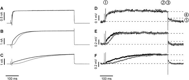
We applied rectangular depolarizing pulses to EAG-expressing HEK 293 cells that covered the gate of a FET (Fig. 1) and recorded simultaneously IM in the whole-cell configuration with a patch pipette and VFET with a FET device. The time course of IM displayed the same characteristics as previously described for voltage-gated EAG currents (15–17) (Fig. 2, A–C).
FIGURE 2.
Comparison of the time course of whole-cell membrane currents (IM) and p-channel FET signals (VFET). (A–C) Whole-cell current recordings for double-pulse activation of the K+ channel from −70 to +50 mV (black traces) and with a hyperpolarizing prepulse to −125 mV (gray traces) using the (A) Ca2+-, (B) Mg2+-, and (C) Co2+ solutions. The prepulse hyperpolarization slowed the activation of EAG channels. This effect was more pronounced in the presence of Mg2+ and Co2+. (D–F) Averaged FET signals VFET (n = 50) recorded with a p-channel FET device (D, Ca2+; E, Mg2+; F, Co2+ solution) with (gray traces) and without a hyperpolarizing prepulse (black traces). The FET recordings display two different signals: fast capacitive signals resulting from the stimulation pulse (1, 3) and slower signals due to the current in the cleft between the attached cell membrane and the transistor surface (2). At the end of the stimulus, an instantaneous decline of VFET (4) that coincides with the negative capacitive transient, and a time-dependent relaxation of the FET signal were observed (5).
We used the following pulse protocol to study the cell-transistor contact: the voltage was first stepped from the holding voltage Vh = from −70 to +50 mV. This step probed the fast activation mode of the EAG channel. After returning to Vh, the cell was hyperpolarized (−125 mV for 500 ms) to promote the transition to the slow activation mode, followed by a short step to Vh (10 ms) and then by a step to +50 mV to activate the channel. The short step to Vh was applied to compare the capacitive transients of the FET signals. To facilitate comparison, the membrane currents activated without (Fig. 2, A–C, black traces) and with hyperpolarizing prepulses (A–C, gray traces) are superimposed in Fig. 2. In the presence of the Ca2+ solution, the hyperpolarizing prepulse had a small but noticeable effect on the rise time of the K+ current (Fig. 2 A, compare black and gray traces). However, in the presence of Mg2+ or Co2+, the slow activation kinetics became very pronounced (Fig. 2, B and C). Co2+ was more effective than Mg2+ in slowing channel activation.
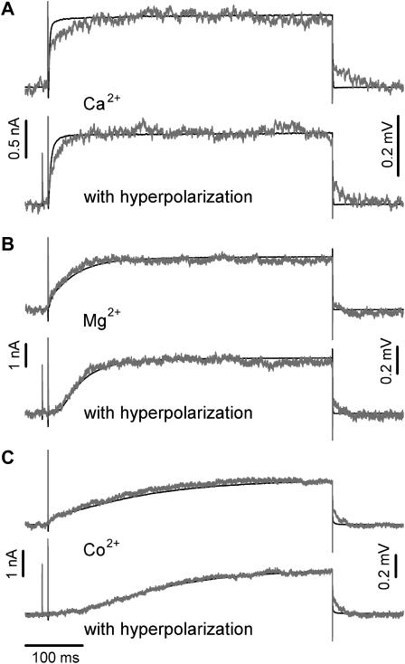
Fig. 2 (D–F) shows FET signals using the Ca2+-, Mg2+-, and Co2+ solutions. To enhance the S/N ratio, the FET recordings were averaged (n = 50). The fast transient signals at the onset (Fig. 2 D, 1) and the offset (3) of the voltage pulses were caused by the coupling of the rectangular stimulation pulses to the capacitance of the attached cell membrane (8,9). The VFET amplitude reached a steady state during stimulation (2). At the end of the stimulation pulse, an instantaneous decline of VFET (4) coincides with the negative capacitive transient (3) followed by a slower relaxation of VFET to the original value (5). Fig. 3 compares the whole-cell patch-clamp currents (black traces) and FET recordings (gray traces) in the presence of the Ca2+-, Mg2+-, and Co2+ solutions. The time courses of the whole-cell currents and the FET signals were similar, except for conditions of fast current activation in the Ca2+ solution and fast deactivation due to the rapid closure of the EAG channel.
FIGURE 3.
Comparison of whole-cell membrane currents and p-channel FET signals (VFET) for different electrolyte solutions with and without a hyperpolarizing prepulse. (A) Ca2+ solution, time course of IM (black traces) and the corresponding averaged VFET (n = 50) (gray traces). (B) Mg2+ solution and (C) Co2+ solution. The recordings with a hyperpolarizing prepulse are indicated.
Extracellular recordings with an n-channel FET
To further investigate the extracellular voltage signals, we used n-channel FETs in addition to p-channel FETs. The higher charge-carrier mobility of n-channel FETs results in a higher transconductance and, in combination with the lower noise level of the buried channel device, in an improved S/N ratio. In contrast to the p-channel FET, n-channel FETs are operated in the first quadrant of the transfer characteristics in which VGS is positive.
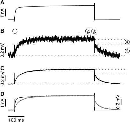
Fig. 4 A shows a typical whole-cell recording from a HEK 293 cell attached to an n-channel FET. A depolarizing voltage pulse led to fast EAG channel activation. The corresponding VFET signal is shown in Fig. 4 B. Due to the significantly higher S/N ratio of the n-channel FET, averaging of signals was not necessary. In fact, the S/N ratio of averaged n-channel recordings (n = 25; Fig. 4 C) was almost as good as that of the patch-clamp recordings. The capacitive transients at the onset (Fig. 4 B, 1) and at the offset of the stimulus (3), and the increase of the VFET amplitude to a steady state (2) are readily identified. Similar to p-channel FETs, the signal at the end of the activation pulse displayed two kinetic components: an instantaneous decline of VFET (4) that coincides with the negative capacitive transient, and a slower relaxation to the initial value (5). The time course of the patch-clamp recording (Fig. 4 D, black trace) was different from that of the superimposed averaged FET recordings (Fig. 4 D, gray trace).
FIGURE 4.
Comparison of whole-cell membrane currents and FET signals VFET recorded with an n-channel FET. (A) Whole-cell current recording using a Ca2+ solution. (B) Nonaveraged n-channel FET signal. The numbers have the same meaning as in Fig. 2, D–F. (C) Averaged FET signal (n = 25). The signal/noise ratio of averaged signals is almost as good as that of whole-cell current recordings. (D) Superposition of IM (black trace) and averaged FET signals (n = 25) (gray trace).
Simulation of FET signals
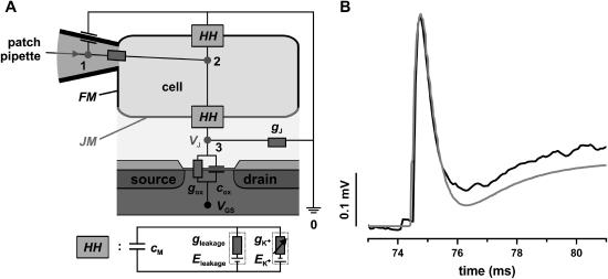
We attempted to fit VFET with a simple equivalent electrical circuit model, the point-contact model (Fig. 5 A) (10). This circuit was implemented in a standard simulation program for electrical circuits (PSpice 9.1 student version, Cadence Design Systems, San Jose, CA) (30). The circuit consists of capacitors, resistors, and current and voltage sources. The stimulating voltage pulse of the patch-clamp pipette VM and the whole-cell membrane current IM were used as voltage and current sources of the simulation circuit (input sources). The model rests on several assumptions.
FIGURE 5.
Point-contact model of cell-transistor coupling. (A) The equivalent electrical circuit of the point-contact model has been implemented for signal simulation in PSpice. The patch pipette is attached in the whole-cell mode. The cell membrane is divided into free (FM) and attached membrane (JM) with a ratio of 2:1 (30) with the respective values of membrane area (AFM, AJM) and membrane capacitance (CFM, CJM). Hodgkin-Huxley elements (HH) (34) describe the properties of the cell membrane and the voltage-gated EAG channels. Cox and Rox = 1/Gox are the capacitance and the resistance of the gate oxide, respectively. VGS is the applied voltage between gate and source. The gate is set to ground contact (point 0). In the point-contact model, the current at the point contact (point 3) between cell and transistor are summed up according to Kirchhoff's law. The voltage is applied between point 1 and point 0 (ground contact). The membrane current flows from point 2 to point 0 for the free membrane, and from point 2 to point 3 for the attached cell membrane. A resistor with the conductance gJ from point 3 to point 0 is used to represent the electrical properties of the cleft between the membrane and the transistor. Using the voltage and current signals as input sources, and the respective capacitances and resistances of the patch pipette and the cell membrane, we obtained the simulated FET signals as the voltage VJ between point 3 and point 0. (B) FET recording (black trace) and simulated FET signal (gray trace). We varied gJ, according to Eq. 2 until the simulated signals matched the recorded signals in amplitude and time course.
First, the contact between the cell and the transistor surface is described by a single point. Second, changes in the ion concentration in the cleft between cell and transistor are neglected. Third, both capacitive and membrane currents flow across the conductance GJ in the cleft (30). Fourth, no capacitive current is flowing across the gate; this assumption holds for small signals, because of the high input impedance of the device. Fifth, the seal resistance of the cleft (RJ), with RJ = 1 / GJ, is at least two orders of magnitude smaller compared to the resistance of the gate oxide (Rox = 0.1–1 GΩ (31)). Therefore, the current across the gate can be neglected in the signal simulation. We further assumed a ratio of 2:1 between the area of free membrane (FM) and membrane in the junction (JM) (30). However, the simulation is largely independent of the FM/JM ratio, because the parameters for all circuit elements have been normalized to the membrane area, i.e., these parameters represent specific values. Even a ratio of 1:1 does not significantly affect the simulated signals (30).
Only a fraction of the total membrane current IM is flowing across the seal resistance (IJM = 0.33 × IM), resulting in a voltage at the point contact (VJ = RJ × IJM). In the point-contact model, all currents entering or leaving the contact point are summed up (12):
 |
(1) |
In this equation, gJ refers to the specific cleft conductance (13);  and
and  refer to the specific conductance of the attached cell membrane and the reversal voltage for the ion species i, respectively, VM and cM refer to the applied membrane voltage and the specific membrane capacitance, respectively. According to Eq. 1, changes in the voltage VJ(t) can be caused by both the membrane current and the capacitive current.
We have determined gJ from the capacitive transients observed in the FET recordings (e.g., Fig. 2 D, 1 and 3) (30):
 |
(2) |
here,  denotes the peak amplitude of the capacitive transients of the VFET recording. In the PSpice simulation, we varied
  to adjust the amplitude of the simulated signal trace to the VFET transients (Fig. 5 B, black trace). We modified gJ according to Eq. 2 until simulated and recorded transients matched (Fig. 5 B, gray trace). The low-pass characteristics of the amplifier circuit, which results in a smaller amplitude of the capacitive transients, have been considered in the simulation. Using the applied VM, the recorded IM, and the adjusted gJ (Eq. 2) as input sources, we obtained the simulated FET signals as the voltage VJ (t) between point 3 and point 0 (ground contact), i.e., VJ at the contact point (Fig. 5 A). A more comprehensive description of the signal simulation using PSpice can be found elsewhere (30).
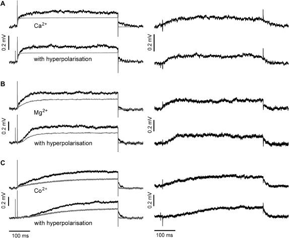
We compared the simulated signals VJ (Fig. 6, gray traces) with the p-channel VFET (Fig. 6, black traces) recorded in different electrolyte solutions (A: Ca2+; B: Mg2+; C: Co2+). The values for the conductance gJ ranged from 0.2 to 3.2 S/cm2 (n = 28). Similar values have been reported for cell-transistor coupling using hippocampal neurons (gJ = 0.6–1.7 S/cm2) (13) and neurons from the brain stem of rats (gJ = 0.3–0.9 S/cm2) (30). Under all conditions, the simulation predicts VJ signals that are ∼60% of the total VFET amplitude (Fig. 6, A–C, left panels). Similar discrepancies have been previously interpreted to be caused by accumulation (or depletion) of ion channels in the membrane area that is attached to the transistor surface (13). The differences between VFET and VJ (Fig. 6, right panels) show almost no fast FET signal component. Therefore, the point-contact model seems to describe the fast FET signal quite accurately. In fact, the predicted steady-state amplitude is 90 ± 34% (n = 28) of the observed fast FET component.
FIGURE 6.
Comparison of recorded FET signals (VFET) and simulated FET signals (VJ) (left panels) and differences of VFET − VJ (right panels). Recorded FET signals (black traces) and simulated FET signals (gray traces) for (A) Ca2+-, (B) Mg2+-, and (C) Co2+ solution. In the right panel, the differences between VFET and VJ show almost no residual fast component of the FET signal.
Comparison of p- and n-channel FET recordings
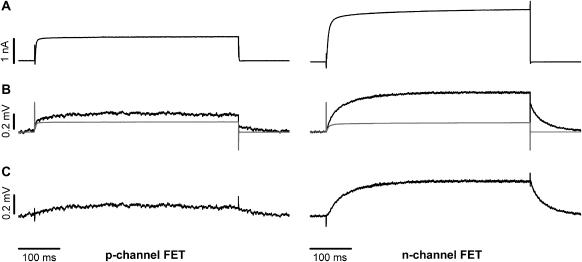
Fig. 7 compares patch-clamp recordings and VFET signals from p-channel (left panels) and n-channel FETs (right panels) using the Ca2+ solution. The membrane currents IM are shown in panel A; the recorded (black traces) and simulated FET signals (gray traces) are shown in panel B; the difference between the recorded and simulated FET signals (VFET − VJ) is shown in panel C. The waveforms of the VFET signals from both FET types are qualitatively similar (compare Figs. 2 and 4). Both signals embody a fast kinetic component that is well described by the point-contact model that predicts 90 ± 34% (n = 28) for the p-channel FETs, and 87 ± 26% (n = 7) for the n-channel FETs, and an additional slow component that is not observed in the whole cell current. The difference of VFET and VJ displays no remaining fast component (Fig. 7 C). The slow component is significantly larger and slower for n-channel FETs than for p-channel FETs. On average the slow component of the n-channel FET signal is 1.8 ± 0.4 times larger then the respective p-channel FET signal component.
FIGURE 7.
Comparison of whole-cell membrane currents (IM) and FET signals (VFET) recorded with a p-channel FET (left panels) and an n-channel FET (right panels). (A) Whole-cell current. (B) Comparison of averaged VFET signals (gray traces) and simulated VJ (black traces). The steady-state ratio VJ/VFET was 60% for the p-channel FET and 25% for the n-channel FET. (C) Difference between recorded and simulated FET signals (VFET − VJ).
DISCUSSION
We chose a cell line expressing EAG channels to characterize the mechanism of cell-transistor coupling. The activation kinetics of EAG channels can be manipulated by voltage and divalent cations. We used this system to investigate whether the transistor signal faithfully recapitulates the features of the ionic membrane current. We made the following key observations. First, the response time of the FETs is sufficient to record the fast capacitive transients at the onset and offset of the stimulating pulse. Second, the time course of the transistor signal VFET is slower than the time course of EAG channel activation in the fast mode, but closely follows the time course of the channel activation in the slow mode. Third, the decline of the transistor signal at the end of the stimulating voltage pulse displays a slow kinetic component that is absent in the instantaneous drop of the whole-cell current. Fourth, n-channel and p-channel transistor signals display distinct time courses. Fifth, the signals of n-channel FETs are significantly larger compared to p-channel signals. Finally, the amplitudes of recorded and simulated transistor signals do not match.
Previous reports explained the discrepancies between recorded and simulated FET signals by the unequal distribution of ion channels between the site of cell-transistor contact and the free membrane (13,14). However, this interpretation neither explains the differences between the n-channel and p-channel FET signals nor the differences in the time course of IM and VFET. We reasoned that the VFET might be affected by changes in ion concentrations in the small cleft between the attached membrane and the semiconductor. The gate oxide of semiconductor devices displays a certain ion sensitivity SFET. This ion sensitivity is most pronounced for protons, however, K+- and Na+-sensitivities have been reported as well (25). If the concentration changes in the cleft were substantial, the surface potential of the gate oxide may be altered giving rise to the additional voltage changes.
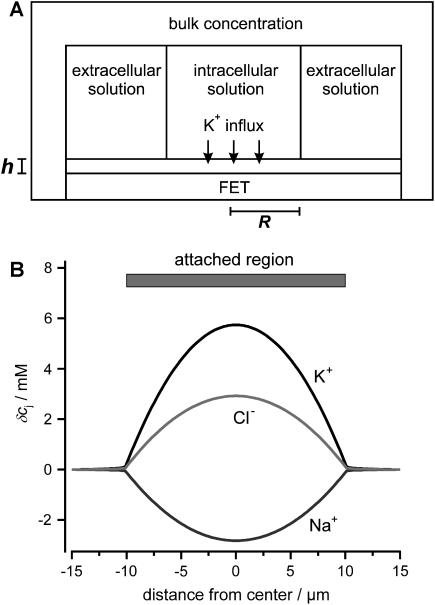
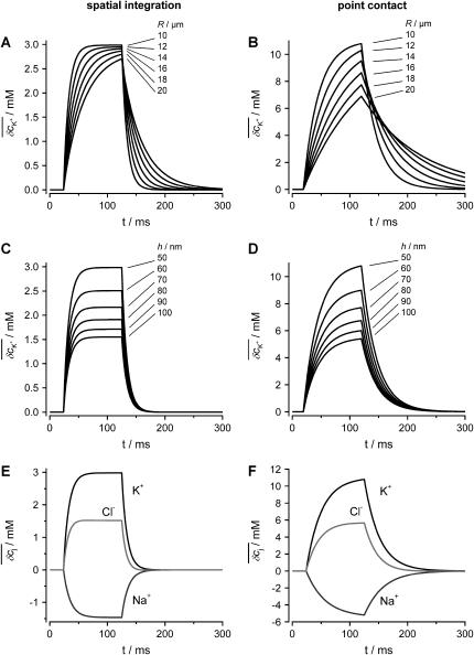
We estimated the changes in ion concentration in the cleft (δcj, j = K+, Na+, and Cl−) by solving the coupled Nernst-Planck and Poisson equations (see Appendix). We assumed a circular attached region with radius R and distance h from the cell surface to the gate oxide. Fig. 8 B shows the profile of the concentration changes of K+, Na+, and Cl− that arise in the attached region after a 100-ms injection of K+ into the cleft. The concentration change of the ions is largest in the center of the attached region and declines toward the periphery. The overall charge is balanced by concomitant concentration changes of K+, Na+, and Cl−. Considering that the effective gate length of the FET (1–2 μm) is significantly smaller than the dimensions of the attached membrane, the question arises to what extent the concentration changes would actually be effective at the gate of the FET. To evaluate this point we integrated the calculated concentration profiles over the cleft volume to obtain a mean  In addition, we reasoned that it might be instructive to compare these results with simplified calculations that better approach the idea of the point-contact model (see Appendix). In the sense of the point-contact model, all ions that diffuse from the cleft to the bulk solution and vice versa have to flow from or to the center of the cleft. We systematically varied the radius R (Fig. 9, A and B) of the attached membrane and the height h of the cleft (Fig. 9, C and D) to estimate the influence of these parameters for the calculated concentration changes. Size and kinetics of
  critically depend on the dimensions of the attached region. An attached region with larger radius significantly slows down the time course of the concentration changes (Fig. 9, A and B). In contrast, variation in h leads to substantial differences in the steady-state amplitudes of
  (Fig. 9, C and D). If we compare the concentration changes for K+, Na+, and Cl− for the spatial integration (Fig. 9 E) and the point-contact approximation (Fig. 9 F), we observe significant differences: The simulated
  are larger and the time course is slower in the point-contact approximation compared to the spatial integration. In fact, the steady-state amplitude of
  in the point-contact approximation is more than twice the size of the peak δcj in the center of the cleft when the spatial integration is used (compare Figs. 8 B and 9 F). Therefore, we conclude that the point-contact approximation is not sufficient to predict the concentration changes in the cleft.
FIGURE 8.
Concentration changes in the attached region. (A) Geometry used for the numerical integration. (B) Profile of the change in ion concentration (δcj) after a 100-ms step injection of K+ into the cleft. The following parameters were used for the calculations: cellular holding voltage Vh = +50 mV, whole cell K+ current IM = 2 nA, R = 10 μm, h = 50 nm, ratio 2:1 of free/attached membrane, bulk concentrations: [K+] = 5 mM, [Na+] = 140 mM, [Cl−] = 145 mM.
FIGURE 9.
Concentration changes in the attached region. (A and B) Impact of radius R of the attached membrane on the amplitude and time course of K+ concentration changes in the cleft for the spatial integration (A) and the point-contact approximation (B). The values of R are indicated in the figure. The following parameters were used for the calculations: cellular holding voltage Vh = +50 mV, whole cell K+ current IM = 2 nA for 100 ms, h = 50 nm, ratio 2:1 of free/attached membrane, bulk concentrations: [K+] = 5 mM, [Na+] = 140 mM, [Cl−] = 145 mM. (C and D) Impact of cleft height h on the amplitude and time course of K+ concentration changes in cleft for the spatial integration (C) and the point-contact approximation (D). Values for h are indicated in the figure; R = 10 μm. Other parameters as in panels A and B. (E) Time course of  for the spatial integration. Parameters as in panels A and B. (F) Time course of
  for the point-contact approximation. Parameters as in panels A and B; R = 10 μm.
We now used the model calculations to estimate the slow component of the FET recordings. We calculated  by integrating the concentration profiles over the cleft volume, but now we used for the current injection a fraction of the EAG whole-cell currents. Using these values of
  we determined the potential
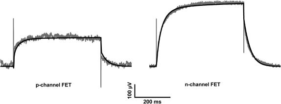
  that reflects the ion sensitivity of the FET device. We only considered the K+ sensitivity, because the relative concentration changes of the other ions are small and will not lead to significant potential changes. We experimentally determined the K+ sensitivity for the p-channel FET (SFET = 0.7 mV/pK, see Materials and Methods). Unfortunately, for the n-channel FET we were not able to determine the SFET value due to drift problems during the recordings. In Fig. 9 the simulation of the FET signals are compared with the respective VFET recording. Here, we combined Vis with the respective VJ from the PSpice simulation. We iteratively adjusted the radius R and the distance h to match the amplitude and kinetics of the slow FET component. For both, the p-channel FET and the n-channel FET, we obtained parameter sets that result in an appreciable simulation of the FET voltage (Fig. 10). For the n-channel FET, we had to additionally assume a slightly higher ion sensitivity to recapitulate VFET. A closer inspection of the parameter sets reveals that the assumed radius R of the attached membrane (R = 19 μm) is somewhat above the mean radius of HEK 293 cells. This high value was necessary to approach the kinetics of the slow FET signal component. However, it should be noted that we neglected the possibility that binding of K+ to the gate oxide may occur with slow dynamics. No data about these kinetics are available. Therefore, we note that the radius R reported here is an upper estimate. In addition, the height of the cleft is with 39 nm for the n-channel FET and 28 nm for the p-channel FET at the lower limit of what has been reported for cell-semiconductor distances (12–105 nm (14,32,33)). As mentioned above, the actual concentration change experienced by the gate of the FET depends on the location of the gate within the attached membrane. In the steady state,
  and the peak δcj in the center of the cleft differ by a factor of almost 2 (compare Figs. 8 B and 9 A). Our calculations would give larger Vis values when the gate was located in the center of the cleft. In that case, we would obtain larger values of the distance h in our VFET simulations.
FIGURE 10.
Comparison of recorded (gray traces) and calculated FET signals (black traces) for a p-channel FET (left panel) and an n-channel FET device (right panel). Each calculated trace represents the sum of the respective PSpice simulation VJ and the additional component Vis due to the ion sensitivity of the FETs. (Left panel) PSpice simulation and results from the spatial integration for the p-channel FET experiment of Fig. 7. Parameters used are: R = 19 μm, h = 28 nm, SFET = 0.7 mV/pK. (Right panel) PSpice simulation and results from the spatial integration for the n-channel FET experiment of Fig. 7. Parameters used are: R = 19 μm, h = 39 nm, SFET = 1.62 mV/pK.
In summary, we propose that at least two different mechanisms contribute to the observed FET signals. When channels in the attached membrane open, an electrical signal component is observed, which depends on the seal resistance RJ. The time course of this component closely follows channel activation and deactivation. This component is readily observed as the “fast component” of the FET signal at the end of the activating voltage pulse and can be well described by our PSpice simulation using Eq. 1. We find that the PSpice simulation accounts for 90% (n = 28) of the fast component for the p-channel FET and 87% (n = 7) for the n-channel FET. Second, for prolonged activation of EAG channels, the ion concentrations in the cleft will change. This gives rise to a change in the surface potential of the gate oxide. This potential rises and declines with a much slower time course than the first, fast component, and explains the slow relaxation of VFET upon channel closure. However, the differences between n- and p-channel FET signals are not adequately described by these additional potential changes. The amplitudes of the slow component of n-channel FET signals were consistently larger than those for p-channel FETs. Moreover, the signal relaxation after channel closure was slower for n-channel FETs than for p-channel FETs. Our calculations indicate that the ion sensitivity of n- and p-channel FETs may be different. However, we cannot exclude the possibility that other mechanisms contribute to the FET signals. Notwithstanding, our study provides a framework for the understanding of processes at the cell-transistor interface by including diffusional and chemical effects.
Acknowledgments
We acknowledge M. Pabst (ISG2) for the discussions, which helped us to develop the presented model. The authors thank W. Knoll, M. Krause, and D. Richter (Max-Planck Institute for Polymer Research, Mainz, Germany) for technical support and for their initial contributions to this project. We acknowledge M. Bruns (IBI1), R. Otto, and S. Schaal (ISG2, Research Centre Jülich) for their support with cell culture, amplifier systems, and FET devices.
This project was supported by the Northrhine-Westfalian Ministry of School and Education, Science and Research, Düsseldorf (H.E.), and by the German Federal Ministry of Education and Research, Berlin, (project No. 0310895).
APPENDIX
To estimate the concentration changes of the ions in the cleft between cell and semiconductor, the coupled Nernst-Planck equations, describing the diffusion of the ionic species within an electric field, and the Poisson equation, describing the dependence of the electric field on the net charge distribution, have to be solved simultaneously. The Nernst-Planck equations are given by
 |
(A1) |
where the cj are concentrations, ψ is the electrostatic potential, Dj are diffusion coefficients, zj electric valences, F and R are Faraday's constant and gas constant, respectively, T is the temperature, and qj are source terms. The index j stands for K, Na, or Cl, respectively. The Poisson equation reads
 |
(A2) |
where ɛ is the dielectric constant of the solution. The only nonvanishing source term is the potassium influx through the cell membrane into the cleft between cell and FET. The full analysis of this problem is numerically challenging, due to the different timescales of the involved processes charge relaxation and diffusion. To better elucidate that point we rewrite Eq. A1 in the form
 |
(A3) |
where the  are the equilibrium bulk concentrations, the δcj are deviations from these bulk concentrations, and we have replaced the Laplacian of the electric potential by the help of the Poisson equation. In the presence of even slight net charges (nM), the third term in Eq. A3 becomes by orders of magnitudes larger than the first two terms, leading to a fast charge relaxation towards electroneutrality on a nanosecond timescale. We will employ this fact and will use a reduced integration scheme, which assumes that the fast relaxation towards equilibrium proceeds full way until electroneutrality is reached, thus ignoring the second term in Eq. A3. Then, the integration can be done in a two-step fashion; for every time step Δt of integration, the injected potassium ions Δt × qK initiate a fast charge relaxation towards electroneutrality, following the equation
 |
(A4) |
after which the dynamics is governed by pure diffusion:
 |
(A5) |
This significantly simplifies the numerical evaluation, lifting the need for the explicit computation of the electrostatic potential by solving the Poisson equation. The electroneutrality limit of Eq. A4 can be found by setting the left-hand side to zero and solving the resulting algebraic problem. A further simplification can be made by ignoring the spatial distribution of different ion concentrations along the cleft radius, and switching to the so-called point-contact approximation by integrating the diffusion equations over the cleft,
 |
(A6) |
where  are the average concentrations within the cleft, and R is the radius of the cleft. The gradient of the concentrations is approximated by
 |
(A7) |
We used both the point-contact model approximation as well as the full integration of Eq. A5 for modeling and fitting the data. Equation A5 was solved by a standard finite-element integration scheme, assuming impenetrable boundaries for the cell membrane and the FET surface, and keeping the concentrations fixed at their bulk concentration values (δcj = 0) at the outer boundaries of the integration region (see Fig. 8 A). The integration region (extracellular space excluding the cleft) was divided into square finite elements of 200-nm edge size; the integration time step was equal to 4 μs. In the point-contact approximation, the integration time step was chosen to be 1 ms. No changes in the numerical results were discernible when further decreasing finite-element size or integration time step.
Fixed parameters used for the calculations: ɛ = 80, T = 309.15 K, DK = 1.96 × 10⁻⁵ cm2/s, DNa = 1.33 × 10⁻⁵ cm2/s, DCl = 2.02 × 10⁻⁵ cm2/s.
G. Wrobel and R. Seifert contributed equally to this work.
References
- 1.Gross, G. W., W. Y. Wen, and J. W. Lin. 1985. Transparent indium-tin oxide electrode patterns for extracellular, multisite recording in neuronal cultures. J. Neurosci. Methods. 15:243–252. [DOI] [PubMed] [Google Scholar]
- 2.Fromherz, P., A. Offenhäusser, T. Vetter, and J. Weis. 1991. A neuron-silicon junction: a Retzius cell of the leech on an insulated-gate field-effect transistor. Science. 252:1290–1293. [DOI] [PubMed] [Google Scholar]
- 3.Bergveld, P., J. Wiersma, and H. Meertens. 1976. Extracellular potential recordings by means of a field-effect transistor without gate metal, called OSFET. IEEE Trans. Biomed. Eng. 23:136–144. [DOI] [PubMed] [Google Scholar]
- 4.Jenkner, M., B. Müller, and P. Fromherz. 2001. Interfacing a silicon chip to pairs of snail neurons connected by electrical synapses. Biol. Cybern. 84:239–249. [DOI] [PubMed] [Google Scholar]
- 5.Zeck, G., and P. Fromherz. 2001. Noninvasive neuroelectronic interfacing with synaptically connected snail neurons immobilized on a semiconductor chip. Proc. Natl. Acad. Sci. USA. 98:10457–10462. [DOI] [PMC free article] [PubMed] [Google Scholar]
- 6.Fromherz, P., and A. Stett. 1995. Silicon-neuron junction: capacitive stimulation of an individual neuron on a silicon chip. Phys. Rev. Lett. 75:1670–1674. [DOI] [PubMed] [Google Scholar]
- 7.Bergveld, P. 1970. Development of an ion-sensitive solid-state device for neurophysiological measurements. IEEE Trans. Biomed. Eng. 17:70–71. [DOI] [PubMed] [Google Scholar]
- 8.Schätzthauer, R., and P. Fromherz. 1998. Neuron-silicon junction with voltage-gated ionic currents. Eur. J. Neurosci. 10:1956–1962. [DOI] [PubMed] [Google Scholar]
- 9.Sprössler, C., M. Denyer, S. Britland, A. Curtis, W. Knoll, and A. Offenhäusser. 1999. Electrical recordings from rat cardiac muscle cells using field-effect transistors. Phys. Rev. E. 60:2171–2176. [DOI] [PubMed] [Google Scholar]
- 10.Regehr, W. G., J. Pine, C. S. Cohan, M. D. Mischke, and D. W. Tank. 1989. Sealing cultured invertebrate neurons to embedded dish electrodes facilitates long-term stimulation and recording. J. Neurosci. Methods. 30:91–106. [DOI] [PubMed] [Google Scholar]
- 11.Weis, R., B. Muller, and P. Fromherz. 1996. Neuron adhesion on a silicon chip probed by an array of field effect transistors. Phys. Rev. Lett. 76:327–330. [DOI] [PubMed] [Google Scholar]
- 12.Fromherz, P. 1999. Extracellular recording with transistors and the distribution of ionic conductances in a cell membrane. Eur. Biophys. J. 28:254–258. [DOI] [PubMed] [Google Scholar]
- 13.Vassanelli, S., and P. Fromherz. 1999. Transistor probes local potassium conductances in the adhesion region of cultured rat hippocampal neurons. J. Neurosci. 19:6767–6773. [DOI] [PMC free article] [PubMed] [Google Scholar]
- 14.Straub, B., E. Meyer, and P. Fromherz. 2001. Recombinant maxi-K channels on transistor, a prototype of iono-electronic interfacing. Nat. Biotechnol. 19:121–124. [DOI] [PubMed] [Google Scholar]
- 15.Terlau, H., J. Ludwig, R. Steffan, O. Pongs, W. Stühmer, and S. H. Heinemann. 1996. Extracellular Mg2+ regulates activation of rat EAG potassium channel. Pflugers Arch. 432:301–312. [DOI] [PubMed] [Google Scholar]
- 16.Frings, S., N. Brüll, C. Dzeja, A. Angele, V. Hagen, U. B. Kaupp, and A. Baumann. 1998. Characterization of ether-a-go-go channels present in photoreceptors reveals similarity to IKx, a K+ current in rod inner segments. J. Gen. Physiol. 111:583–599. [DOI] [PMC free article] [PubMed] [Google Scholar]
- 17.Tang, C. Y., F. Bezanilla, and D. M. Papazian. 2000. Extracellular Mg2+ modulates slow gating transitions and the opening of Drosophila ether-a-go-go potassium channels. J. Gen. Physiol. 115:319–337. [DOI] [PMC free article] [PubMed] [Google Scholar]
- 18.Schönherr, R., L. M. Mannuzzu, E. Y. Isacoff, and S. H. Heinemann. 2002. Conformational switch between slow and fast gating modes: allosteric regulation of voltage sensor mobility in the EAG K+ channel. Neuron. 35:935–949. [DOI] [PubMed] [Google Scholar]
- 19.Offenhäusser, A., C. Sprössler, M. Matsuzawa, and W. Knoll. 1997. Field-effect transistor array for monitoring electrical activity from mammalian neurons in culture. Biosens. Bioelectron. 12:819–826. [DOI] [PubMed] [Google Scholar]
- 20.Krause, M. 2000. Untersuchungen zur Zell-Transistor Kopplung mittels der Voltage-Clamp Technik PhD thesis. (http://archimed.uni-mainz.de). [in German]. Universität Mainz, Mainz, Germany.
- 21.Ingebrandt, S. 2001. Characterisation of the Cell-Transistor Coupling. PhD thesis. (http://archimed.uni-mainz.de). Johannes Gutenberg-Universität Mainz, Mainz, Germany.
- 22.Sprössler, C., D. Richter, M. Denyer, and A. Offenhäusser. 1998. Long-term recording system based on field-effect transistor arrays for monitoring electrogenic cells in culture. Biosens. Bioelectron. 13:613–618. [Google Scholar]
- 23.Ingebrandt, S., C. K. Yeung, W. Staab, T. Zetterer, and A. Offenhäusser. 2003. Backside contacted field effect transistor array for extracellular signal recording. Biosens. Bioelectron. 18:429–435. [DOI] [PubMed] [Google Scholar]
- 24.Ecken, H., S. Ingebrandt, M. Krause, D. Richter, M. Hara, and A. Offenhausser. 2003. 64-Channel extended gate electrode arrays for extracellular signal recording. Electrochim. Acta. 48:3355–3362. [Google Scholar]
- 25.Abe, H., M. Esashi, and T. Matsuo. 1979. ISFET's using inorganic gate thin films. IEEE Trans. Electron Devices. 26:1939–1944. [Google Scholar]
- 26.Chen, C. A., and H. Okayama. 1988. Calcium phosphate-mediated gene-transfer: a highly efficient transfection system for stably transforming cells with plasmid DNA. Biotechniques. 6:632–638. [PubMed] [Google Scholar]
- 27.Hamill, O. P., A. Marty, E. Neher, B. Sakmann, and F. J. Sigworth. 1981. Improved patch-clamp techniques for high-resolution current recording from cells and cell-free membrane patches. Pflugers Arch. 391:85–100. [DOI] [PubMed] [Google Scholar]
- 28.Sigworth, F. J. 1995. Design of the EPC-9, a computer-controlled patch-clamp amplifier. 1. Hardware. J. Neurosci. Methods. 56:195–202. [PubMed] [Google Scholar]
- 29.Sigworth, F. J., H. Affolter, and E. Neher. 1995. Design of the EPC-9, a computer-controlled patch-clamp amplifier. 2. Software. J. Neurosci. Methods. 56:203–215. [DOI] [PubMed] [Google Scholar]
- 30.Ingebrandt, S., C. K. Yeung, M. Krause, and A. Offenhausser. 2005. Neuron-transistor coupling: interpretation of individual extracellular recorded signals. Eur. Biophys. J. 34:144–154. [DOI] [PubMed] [Google Scholar]
- 31.Sze, S. M. 1985. Semiconductor Devices. John Wiley & Sons, Murray Hill, NJ.
- 32.Braun, D., and P. Fromherz. 2000. Membrane voltage map from stimulated single neuron recorded optically on silicon chip. Biophys. J. 78:217a (Abstr.). [Google Scholar]
- 33.Braun, D., and P. Fromherz. 2001. μM and μs resolution in membrane potential imaging reveals seal properties of cells and tissue in 3D. Biophys. J. 80:100a (Abstr.). [Google Scholar]
- 34.Hodgkin, A. L., and A. F. Huxley. 1952. A quantitative description of membrane current and its application to conduction and excitation in nerve. J. Physiol. (Lond.). 117:500–544. [DOI] [PMC free article] [PubMed] [Google Scholar]


