Abstract
We have studied the carrier transport in poly(2,5-bis(3-tetradecylthiophen-2-yl)thieno[3,2-b]thiophene) field-effect transistors (FETs) at very high field-induced carrier densities (1015 cm−2) using a polymer electrolyte as gate and gate dielectric. At room temperature, we find high current densities, 2 × 10⁶ A/cm2, and high metallic conductivities, 104 S/cm, in the FET channel; at 4.2 K, the current density is sustained at 107 A/cm2. Thus, metallic conductivity persists to low temperatures. The carrier mobility in these devices is ≈3.5 cm2·V−1·s−1 at 297 K, comparable with that found in fully crystalline organic devices.
Keywords: conjugated polymer, electronic transport
Starting with the first demonstration of metallic conductivity in chemically doped conjugated polymers (1), there has been considerable interest in realizing a truly metallic state, wherein nonactivated metallic transport persists to low temperatures. Metallic transport, attributed to improved order of the molecular structure, was recently reported by Lee et al. (2) in polyaniline with room temperature conductivities of >103 S/cm. While increasing the density of carriers, however, chemical doping also increases disorder, disrupts the intrinsic density of states (3), and thereby leads to localization of the carrier wavefunctions. This additional source of disorder is eliminated by using the capacitance and gate voltage (Vg) in field-effect transistors (FETs) to induce sufficient carrier densities to reach the metallic regime (4). However, the observation of metallic conduction in the two-dimensional regime within the channel of FETs has been generally limited by both the capacitance and electric field breakdown strength of commonly used gate dielectric materials.
Electrolyte-gate dielectrics, first used by the inventors of the transistor in 1947, can support very high field-induced charge densities compared with conventional dielectrics (5, 6). Indeed, the conductivity of polymer FETs has been shown to be enhanced by several orders of magnitude when a polymer electrolyte is used (7). More recently, Panzer and Frisbie (8) demonstrated high conductivities (103 S/cm) in polymer electrolyte gated polymer devices at carrier densities of ≈1015 cm−2. They assume that an ionic double layer near the interface between the electrolyte and the semiconducting polymer, with charge separation over the nanoscale, is responsible for the exceptionally large field-induced carrier densities. On the other hand, 15 years ago, Wrighton and colleagues (9) carefully examined the in situ doping in electrochemical FETs that utilized liquid electrolyte. Panzer and Frisbie (8) addressed the issue of electrochemical doping by depositing a thin layer of insulating material between the polymer semiconductor and the polymer electrolyte.
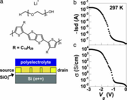
In this work, we use a poly(ethylene oxide)/lithium perchlorate (PEO/LiClO4) polymer electrolyte gate dielectric to study the carrier transport in poly(2,5-bis(3-tetradecylthiophen-2-yl)thieno[3,2-b]thiophene) (pBTTT-C14) FETs at high carrier densities (1015 cm−2), over a temperature (T) range from 298 to 4.2 K. Fig. 1a shows the FET structure used to measure the channel conductivity. A section cut from a heavily n-type doped silicon wafer, covered with a 200- to 300-nm-thick SiO2 layer, is used as the substrate; the polymer electrolyte layer serves as the top gate. The polymer electrolyte used here has been studied in detail elsewhere (ref. 10 and references therein). The channel had a length of 12 μm and a width of 1,000 μm for all devices.
Fig. 1.
Polymer electrolyte gated FET structure and room temperature device characteristics. (a) A schematic illustration of the four-probe device structure complete with the ionic polymer electrolyte layer (Bottom) with the molecular structure shown (Top). The molecular structure of pBTTT-C14 is also shown (Middle). (b and c) Typical current vs. Vg (b) and conductivity vs. Vg (c) data measured for a device in ambient air at room temperature and Vsd = −1 V. The Vg sweep rate was ≈60 mV/s.
In the experiments carried out by Panzer and Frisbie (8), two-probe measurements were used to characterize the transport in polymer electrolyte gated devices by using poly(3-hexylthiophene) as the semiconducting polymer. Here, we use a four-probe configuration, with two long parallel electrodes, each 2 μm wide and 4 μm apart, inside the channel, to enable independent measurements of the channel resistance and contact resistance of the FET. In addition, we use a recently developed liquid crystalline thieno[3,2-b]thiophene polymer, pBTTT-C14 (molecular structure is shown in Fig. 1a), for which field-effect carrier mobilities were reported to be as high as μ = 0.2–0.6 cm2·V−1·s−1 (11).
For field-induced carrier injection, the majority of carriers are confined to a depth of 1–2 nm within the semiconductor; i.e., approximately a monolayer of the semiconducting polymer. All conductivities, σ, were estimated assuming carrier confinement to within a thickness of 1 nm near the gate-dielectric/polymer interface. Thus, within this two-dimensional layer, the carrier density is ≈1022 cm−3. If, on the other hand, the material in the channel has been electrochemically doped by insertion of the perchlorate anions (ClO4−), the carrier density will be distributed approximately uniformly throughout the film thickness. We discuss this possibility in more detail in the following section.
The n-type doped Si substrate is thermally anchored by using a small spot of Apiezon-N thermal grease applied to a sapphire disk inlaid in a copper block that serves as the heat sink. Temperatures were measured by using a Lake Shore Cryotronics sensor, which was In-soldered to the copper block, directly opposite the device.
Results and Discussion
Fig. 1b shows the Vg dependence of the device current typically found at room temperature, at a fixed source–drain voltage of Vsd = −1 V. The source–drain current reaches Isd = −21 mA at Vg = −3 V, corresponding to a current density of 2 × 10⁶ A/cm2. We can expect significant electrical power dissipation into the device at this current density and discuss this point further below. The conductivity in the channel, shown in Fig. 1c, reaches 9,700 S/cm at the highest applied Vg, comparable with the conductivity of conventional metals. The maximum conductivity measured in devices having only a bottom-gate dielectric (SiO2) was ≈1 S/cm at Vg = −140 V (4). Therefore, the electrolyte-gated field effect clearly dominates the device transconductance over the range of voltages measured here.
The carrier mobility μ in the device can be calculated by estimating the polymer electrolyte double-layer capacitance to be C ∼ 100 μF·cm−2 (8). The highest mobility achieved, calculated by using the relation σ = neμ, where n is the areal charge density (CVg) and e is the electronic charge, is μ ≈ 3.5 cm2·V−1·s−1 at Vg = −2.8 V, which is significantly higher than that measured for SiO2-gated devices (11)§ and comparable with the carrier mobilities found in FETs fabricated with organic single-crystal semiconductors (12). The increase in mobility at high carrier densities is qualitatively consistent with the data reported for poly(3-hexylthiophene) devices (8). The high conductivity and high mobility imply band transport rather than hopping through a distribution of localized levels.
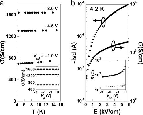
Fig. 2a shows the temperature dependence of the conductivity for varying Vsd, measured in the range 4.2–15 K, for a device that had been first cooled to 4.2 K with the gate bias held constant at Vg = −3 V and with Vsd = 0 V. The data clearly show a weak temperature dependence that implies finite conductivity at T = 0 K, characteristic of metallic behavior. For example, at Vsd = −8 V, the channel conductivity is 1,600 S/cm; therefore, the metallic conductivities observed at room temperature (Fig. 1c) persist down to 4.2 K. At low temperatures (see Fig. 2a Inset), and for all devices at T < 260 K, the channel conductivity is independent of Vg up to the maximum applied voltage, indicating that ionic motion is completely frozen out.
Fig. 2.
Low-temperature device characteristics. (a) Conductivity vs. temperature at varying Vsd for a device cooled beforehand from room temperature to 4.2 K while holding the gate bias constant at Vg = −3 V. (Inset) The conductivity vs. Vg at 4.2 K. (b) Current (and conductivity) vs. source–drain electric field for the same device shown in a, at 4.2 K. (Inset) The channel (filled circles) and contact (open circles) resistance vs. Vsd at 4.2 K.
Fig. 2b shows the dependence of the current and conductivity on the source–drain electric field (E) at 4.2 K. At the highest applied Vsd = −8.6 V, E = 5.8 kV/cm,¶ the current reaches Isd = −98 mA, corresponding to a current density of 107 A/cm2. The ability of the device to support such a high current at low temperatures is remarkable.
Above |Isd| = 43 mA (4 × 10⁶ A/cm2), we find that the temperature of the device (as inferred from the calibrated thermometer mounted on the copper sample holder) begins to increase, indicating Joule heating due to the channel resistance. For example, with the sample holder immersed directly into the liquid helium, the measured temperature increase is ΔT ≈ 60 mK at Isd = −98 mA (Vsd = −8.6 V). Note that there is no change in the measured conductivity when the sample holder is lifted out of the cryogenic liquid, whereas the measured temperature jumps by 1–2 K (see Fig. 2a). The data in Fig. 2b span a range of electrical input power of >3 orders of magnitude. Therefore, although Joule heating is present at the highest current densities measured, it does not significantly change the measured conductivity values.
Fig. 2b Inset shows the Vsd dependence of the channel and contact resistances at 4.2 K. The channel resistance becomes ohmic with increasing Vsd. Note that even at 4.2 K, the contact resistance is small (smaller than that measured at room temperature) and constant over the entire voltage range measured, consistent with the high conductivity of the gate-induced metallic layer in the channel.
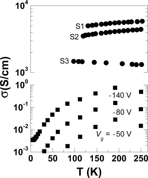
Fig. 3 shows the T-dependent conductivity measured for three polymer electrolyte gated devices and for a single SiO2-gated device with no electrolyte layer (similar data are discussed in ref. 4). We find that although all of the electrolyte-gated devices shown had initially high conductivities (>103 S/cm) at room temperature, their T dependences, measured subsequent to freezing the motion of ions in the electrolyte, are somewhat different. The conductivity for devices S1 and S2 is weakly temperature dependent; e.g., the data for S1 exhibit an activation energy of 3.6 meV. Device S3, on the other hand, shows an increase in conductivity with decreasing temperature, as expected for a metal. The origin of the different T-dependent behavior is unclear and, presumably, is controlled by the nature of the polymer/polymer electrolyte interface. The conductivity data for the SiO2-gated device (lower capacitance and therefore lower carrier density) show stronger T-dependent behavior with an activation energy of 15 meV, between 200 and 50 K, at Vg = −140 V. Therefore, the data unambiguously confirm that the carrier transport is sensitive to the level of field-induced carrier density.
Fig. 3.
Conductivity vs. temperature for three polymer electrolyte gated (circles) devices at Vsd = −1 V. All devices were cooled beforehand to ≈260 K while holding the gate bias constant at Vg = −3 V. The data for a device without the electrolyte layer (squares), gated instead by using the bottom contact (SiO2, 200-nm thick), are shown at fixed Vsd = −60 V and varying Vg.
As noted above, electrochemical oxidation of pBTTT-C14 by the perchlorate anions would significantly alter the charge distribution profile within the transistor channel from that expected for a purely capacitatively coupled device. Although Panzer and Frisbie (8) attempted to rule out electrochemical doping by depositing a thin insulator between the polymer semiconductor and the polymer electrolyte, the possibility of pinholes in the insulating layer is, however, difficult to completely rule out. If the semiconducting polymer were in fact wholly electrochemically doped, the calculated conductivities and current densities given above would be smaller by the ratio of the polymer thickness to that of the assumed accumulation layer.
We note, however, the following: (i) the measured device conductance does not change significantly when the polymer thickness is decreased from 30 to 12 nm;‖ therefore, the spatial extent of any electrochemical doping is not uniform and is instead restricted to a few monolayers near the semiconducting polymer/polymer electrolyte interface; (ii) the persistence of the metallic state at 4.2 K with unprecedented conductivity values and very low activation energies are features uncharacteristic of typical electrochemically doped samples; (iii) the very small, nonactivated contact resistance over the entire temperature regime studied is consistent with a metallic state, with metallic screening at low temperatures; and (iv) given (i), for a sufficiently thin electrochemically doped layer, the charge confinement will approximately resemble that expected in an FET. Hence, the calculated conductivity and current density values are considered to be realistic estimates.
Finally, we carried out the following control experiment: by using an identical device configuration, with poly(3-hexylthiophene) as the active semiconductor, a voltage was applied to the electrolyte gate, and the expected increase in the channel conductance was observed. The electrolyte then was removed by using an acetone, isopropanol wash, and the device was tested again (Isd vs. Vg) by using SiO2 as the gate dielectric and the doped Si substrate as the gate electrode. There was no evidence of electrochemical doping in the bulk of the film; the maximum source-drain current (Isd) was in the microampere range both before and after charging and then removing the electrolyte gate. In addition, after removing the electrolyte either by the acetone, isopropanol wash or by using adhesive tape, no significant color change in the polymer was observed. Thus, we found no indication of electrochemical doping in the bulk of the semiconducting polymer film. We speculate that the low mobility of the ClO4− within the poly(ethylene oxide) host inhibits p-type electrochemical doping.
In conclusion, we have confirmed metallic field-induced charge carrier densities in polymer FETs by using a polymer electrolyte gate dielectric (8). Four-probe measurements yield conductivities as high as 104 S/cm at room temperature, with an estimated carrier mobility of μ ≈ 3.5 cm2·V−1·s−1. The metallic state persists to low temperatures. At 4.2 K, remarkably high current densities, 107 A/cm2, are sustained in the device channel, without noticeable degradation.
The use of the polymer electrolyte gate dielectric creates an opportunity for exploring a wide variety of materials for the detailed investigation of formerly unreachable transport regimes. One must, however, be careful in every case to consider the possibility of electrochemical doping.
Materials and Methods
Devices were fabricated on heavily n-type doped silicon substrates covered with a 200- to 300-nm-thick SiO2 layer. The source, drain, and gate contacts were metallized by using 50 nm of Au with a 5-nm-thick Ti adhesion layer. The polymer was dissolved into 1,2-dichlorobenzene (Sigma-Aldrich) at a concentration of 5 mg/ml and deposited by spin coating onto an octadecyltrichlorosilane (1% dilution in toluene) pretreated substrate from a warm solution at 3,000 rpm for 60 s in a nitrogen-filled glove box. Devices were annealed on a hot plate at 160°C in the glove box for 10 min. Typical film thickness was 30 nm (measured by using a Filmetrics F20 analyzer). For the polymer electrolyte, LiClO4 (Fluka) was added to poly(ethylene oxide) (Sigma-Aldrich), average Mv ∼ 100,000, in a 1:1.36 by weight ratio and dissolved in acetonitrile (Sigma-Aldrich) at a concentration of 30 mg/ml. The final solution was obtained by passing through a 0.2-μm polytetrafluoroethylene (PTFE) filter. Devices were completed by drop-casting the electrolyte directly onto the polymer layer and left overnight under vacuum to dry. Devices were measured by using Keithley Sourcemeters (Model 2400), with internal impedance of >1010 Ω. Temperature was varied from 298 to 4.2 K by dipping the device into a dewar containing liquid helium. The lowest temperature (4.2 K) data were obtained by immersing the device directly into the cryogenic liquid.
Acknowledgments
We thank Dr. S. Cho and J. Swensen for valuable discussions regarding the possibility of electrochemical doping. This work was supported by the National Science Foundation and the Heeger Center for Advanced Materials at the Gwangju Institute of Science and Technology (GIST) in Gwangju, Korea.
Abbreviations
- FET
field-effect transistor
- pBTTT-C14
poly(2,5-bis(3-tetradecylthiophen-2-yl)thieno[3,2-b]thiophene).
Footnotes
Conflict of interest statement: No conflicts declared.
We measure a field-effect mobility in the saturation regime of 0.1 cm2·V−1·s−1 at 296 K in ambient air, using the SiO2 as the gate dielectric.
The source–drain electric field, E, across the transistor channel is the measured four-probe voltage across the channel divided by the effective channel length.
The thinner polymer film was deposited by spin coating from a lower-weight-concentration pBTTT-C14 solution.
References
- 1.Chiang C. K., Fincher C. R., Park Y. W., Heeger A. J., Shirakawa H., Louis E. J., Gau S. C., Macdiarmid A. G. Phys. Rev. Lett. 1977;39:1098–1101. [Google Scholar]
- 2.Lee K., Cho S., Heum Park S., Heeger A. J., Lee C.-W., Lee S.-H. Nature. 2006;441:65–68. doi: 10.1038/nature04705. [DOI] [PubMed] [Google Scholar]
- 3.Tal O., Rosenwaks Y., Preezant Y., Tessler N., Chan C. K., Kahn A. Phys. Rev. Lett. 2005;95:256405. doi: 10.1103/PhysRevLett.95.256405. [DOI] [PubMed] [Google Scholar]
- 4.Dhoot A. S., Wang G. M., Moses D., Heeger A. J. , Phys. Rev. Lett. 2006;96:246403. doi: 10.1103/PhysRevLett.96.246403. [DOI] [PubMed] [Google Scholar]
- 5.Bardeen J., Brattain W. H. Phys. Rev. 1948;74:230–231. [Google Scholar]
- 6.Brattain W. H., Garrett C. G. B. Bell Syst. Tech. J. 1955;34:129–176. [Google Scholar]
- 7.Kaneto K., Asano T., Takashima W. Jpn. J. Appl. Phys. 1991;30:L215–L217. [Google Scholar]
- 8.Panzer M. J., Frisbie C. D. Adv. Funct. Mater. 2006;16:1051–1056. [Google Scholar]
- 9.Ofer D., Crooks R. M., Wrighton M. S. J. Am. Chem. Soc. 1990;112:7869–7879. [Google Scholar]
- 10.Bruce P. G., Vincent C. A. J. Chem. Soc. Faraday Trans. 1993;89:3187–3203. [Google Scholar]
- 11.McCulloch I., Heeney M., Bailey C., Genevicius K., Macdonald I., Shkunov M., Sparrowe D., Tierney S., Wagner R., Zhang W. M., et al. Nat. Mater. 2006;5:328–333. doi: 10.1038/nmat1612. [DOI] [PubMed] [Google Scholar]
- 12.Sundar V. C., Zaumseil J., Podzorov V., Menard E., Willett R. L., Someya T., Gershenson M. E., Rogers J. A. Science. 2004;303:1644–1646. doi: 10.1126/science.1094196. [DOI] [PubMed] [Google Scholar]


