Abstract
The large dielectric constant and small effective mass in a semiconductor allows a description of its electronic states in terms of envelope wavefunctions whose energy, time, and length scales are mesoscopic, i.e., halfway between those of atomic and those of condensed matter systems. This property makes it possible to demonstrate and investigate many quantum mechanical, many-body, and quantum kinetic phenomena with tabletop experiments that would be nearly impossible in other systems. This, along with the ability to custom-design semiconductor nanostructures, makes semiconductors an ideal laboratory for experimental investigations. We present an overview of some of the most exciting results obtained in semiconductors in recent years using the technique of ultrafast nonlinear optical spectrocopy. These results show that Coulomb correlation plays a major role in semiconductors and makes them behave more like a strongly interacting system than like an atomic system. The results provide insights into the physics of strongly interacting systems that are relevant to other condensed matter systems, but not easily accessible in other materials.
Understanding many-particle systems is one of the outstanding issues of modern physics. Although condensed matter physics is dominated by the Coulomb interaction only, the problem is extremely complicated, because here we are dealing with very dense systems that comprise N ≈1022 → 1023 particles per cubic cm. This problem is especially delicate when describing the excited states. In that case, however, a popular approach to circumvent the complexity of the problem is to replace the real particles, interacting through the long-range Coulomb force, by a smaller number of fictitious “quasi-particles,” i.e., real particles “dressed” by a part of the Coulomb interaction, which then interact more weakly through mechanisms that originate from the remaining part of that interaction. However, because there is no free lunch (especially in science), the quasi-particles that one ends with are complex objects with an internal structure, interacting among themselves through bizarre effective Hamiltonians and evolving in the background of a new “vacuum,” which is itself dynamical and structured. For example, the effective Hamiltonian describing the quasi-particles can have strange symmetries (as in the case of the fractional Quantum Hall Effect), and the active vacuum can induce strange properties such as spin/charge separation (as in the case of strongly correlated antiferromagnetic materials). Besides the obvious importance of such an approach for understanding the properties of real-life materials, it has the further fundamental interest of giving us the opportunity to test fundamental ideas of quantum mechanics in tabletop experiments, a luxury not given to our high-energy colleagues.
In this context, semiconductors play a very special role in condensed matter physics. These materials have been around for quite some time, a lot is known about their fundamental properties, and sound theoretical techniques, based on well-established approximations, are at hand for describing their ground-state and linear response. Because of their technological importance, very advanced fabrication and processing techniques have been developed, and almost perfect samples and artificial quantum structures are now available. These now allow us to engineer electronic eigenfunctions in a manner not possible in atomic or other condensed matter systems. In these ultra-small structures quantum size effects appear whenever at least one of the sample dimensions becomes of the order of or smaller than a length scale characterizing the quasi-particles. In semiconductors, these complex objects involving many atomic sites can be characterized by envelope wavefunctions whose natural energy, time, and length scales are very different from those of an atomic system, opening new avenues for investigating phenomena, including some fundamental quantum mechanical ones. Observation of such phenomena in atomic systems or on “regular” electrons would require extreme conditions, very difficult if not impossible to obtain in the laboratory. Examples of such changes in scale are given in Box B1 and Box B2. Furthermore, these energy and time scales are well matched to those of state-of-the-art optical and transport spectroscopic techniques. Therefore semiconductors and their nanostructures form a perfect laboratory for extending our field of investigation to regimes previously inaccessible and also serve as model systems for other, more complex condensed matter systems. In this article we review recent progresses made in that direction using the techniques of ultrafast time-resolved nonlinear optical spectroscopy.
Box 1.
Box 1.
Semiconductor Elementary Excitations: Length and Energy Scales
Semiconductor Elementary Excitations: Length and Energy Scales
Box 2.
Box 2.
Quantum Wells, Superlattices, and Related Nanostructures
Quantum Wells.
a-DQWS.
Superlattices.
Quantum Wells, Superlattices, and Related Nanostructures
Quantum Wells.
a-DQWS.
Superlattices.
Time-Resolved Nonlinear Optics
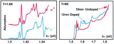
Absorption of low level and constant intensity light by semiconductors reveals a variety of resonances associated with generation of long-lived quasi-eigenstates of the crystal called elementary excitations, such as excitons, polaritons, Fano-resonances, and dressed hole at the origin of Fermi edge singularities (see Box B1). For extremely low-light intensity, the absorption spectrum, such as that shown in Fig. 1, and other optical parameters are independent of the light intensity and can be considered as intrinsic properties of the material. This is the regime of linear optics. This picture changes radically, and one enters the regime of nonlinear optics when the semiconductor is excited by intense laser pulses. These changes occur because high intensity of the pulses can produce very high density of excitations, leading to many-body interactions. Furthermore, the extremely short duration of current laser pulse allows one to explore regimes where Fermi golden rule and Boltzmann kinetics are no longer valid, and the high spectral bandwidths of the pulses allow generation and investigation of electronic wavepackets. These issues are briefly introduced in this section and are illustrated and discussed with the use of recent results in the following sections.
Figure 1.
Optically active elementary excitations in semiconductors. (Left) Absorption edge of bulk GaAs at a B = 12 T magnetic field. The lowest energy peaks are caused by excitons strongly distorted by the magnetic confinement. They are followed by Fano-resonances caused by the quantum interference between the second Landau-edge excitons with the one-dimensional continua of the first one. (Right) Resonances associated with confined excitons and Fermi edge singularity in undoped and modulation-doped quantum well structures.
Excitation of a medium with ultrashort pulses of light creates polarization waves whose quantum mechanical phase initially is defined by that of the laser fields. In the case of a semiconductor, during the first few optical cycles, they oscillate between the valence and conduction bands. However, because these polarization waves are far from being eigenstates of the crystal, in a few tens of fs many-body interactions start between them and the waves associated with the collective excitations, carriers, and phonons present in the sample. Because of these interactions all optical properties become intensity and time dependent; this is the nonlinear optics regime. It is intuitively clear that in this regime the optical response can provide information on the interaction between elementary excitations that is not accessible in linear optics.
A further interesting aspect is related to the time dependence of this response. It is natural to expand the laser-excited polarization waves on the basis set formed by the elementary excitations seen in the linear regime. Then one realizes that, as always in quantum mechanics, the collisions are not instantaneous. They are interferences with time scales defined by the periods of the interacting waves, because a probe, of any sort, cannot distinguish the nature of a wave before interacting with it for a time of the order of one period. As the interactions progress a number of processes begin to be turned on; the lattice begins to react to the appearance of charges (phonons are absorbed or created), and the Coulomb potential starts to be screened (plasmons are absorbed or created). During this transient period the dynamics are highly nonclassical, and well-known theoretical tools, such as the Fermi golden rule or the Boltzmann equation, are inadequate to describe it, and in fact it must be described by quantum kinetics. As scattering processes become effective, the coherence begins to decay and is completely lost after several tens of fs. It is only then that the quasi-particles start to behave in a more usual manner. It is clear that a true quantum mechanical description of the short-time dynamics exhibits a number of novel properties. For example, the scattering processes are not completed and have not yet become irreversible and, because of time-energy uncertainty, the quasi-particle energy is not well defined so that energy conservation is not a meaningful concept for the individual scattering process. For fixing the orders of magnitude we can consider the model material gallium arsenide (GaAs) in which the period of the longitudinal optical (LO) phonon is TLO = 115 fs and a plasma of density n = 5 × 1017 cm−3 has a Tpl ≈ 150 fs-period. Because these times are much longer than the pulses of commercially available lasers, a new regime of interaction dynamics is now accessible to experiments and represents a challenge to our current understanding.
Additional interesting aspects of ultrashort laser pulses are better viewed in the energy domain. Ultrafast lasers have very broad spectra, e.g., the spectral width of a 50-fs laser pulse is approximately 30 meV or 240 cm−1, equivalent to about 15 nm at 800-nm wavelength. This wide spectral width allows a single ultrashort laser pulse to excite a wavepacket, i.e., a linear superposition of the eigenstates, whose dynamics thus is determined by a time-dependent many-body Schrödinger equation. Furthermore, because the relative phase between fs pulses can be controlled to a precision much better than the period of one optical cycle, i.e., about 2.7 fs at 800 nm (see below for some examples), it is possible to coherently control a variety of properties of the semiconductor elementary excitations. The dynamics of the wavepacket evolution and the coherent control of excitations in semiconductors and their nanostructures can be investigated directly by nonlinear optical techniques. Such investigations provide a striking demonstration of fundamental quantum mechanical processes, such as tunneling and wavepacket oscillation, and give new insights into the physics that controls coherence and decoherence in condensed matter.
In Box B3 we illustrate the most frequently used nonlinear optical spectroscopy techniques: pump/probe and coherent wave mixing. The sample is excited by two (or more) ultrafast laser pulses separated by a delay Δt. The first pulse brings the samples in an excited and nonequilibrium state that is probed by the subsequent pulses, thus allowing us to follow directly the dynamics of the processes mentioned above.
Box 3.
Box 3.
Principle of Time-Resolved Nonlinear Optical Spectroscopy Experiments
Principle of Time-Resolved Nonlinear Optical Spectroscopy Experiments
Many-Body Effects and Quantum Kinetics
The coherent wave mixing techniques first were applied to atomic and molecular systems whose spectra consist of well-separated discrete levels. In that case, and limiting ourselves to processes that are third order in the field, for a fixed delay between the two pulses, the coherent wave mixing signal is emitted immediately after the second pulse and corresponds to a free polarization decay, i.e., it is zero for t<t2 and exhibits a simple exponential decay for t>t2 that characterizes the decoherence of the nonlinear polarization waves. As explained in Box B3, STI, the signal measured with a slow detector as Δt is varied and integrates the coherent wave mixing emission. For atomic-like systems this time-integrated signal has, as a function of the delay Δt, the same temporal behavior as that of the coherent wave mixing signal vs. the absolute time t. Because of the historical background of atomic and molecular physics and the simplicity of the two-level atom model, the early ultrashort pulse investigations on semiconductors were analyzed within this framework.
A striking qualitative difference with the ideas commonly accepted in atomic physics was observed when very high-quality heterostructures, with homogeneously broadened exciton resonances, were probed with ultrashort pulses. As shown in Fig. 3, time-integrated four-wave mixing (FWM) experiments revealed a very strong signal, STI(Δt), for Δt<0, extending at least as far as 20 times the laser pulse duration before Δt = 0 and with a rise time half the decay time. This direct contradiction with the atomic theories forced a re-evaluation of the analysis of coherent optical processes in semiconductors to account for two-particle correlation. In an atomic system the only source of nonlinearity is the result of the Pauli principle, an effect active for all material systems, atoms, molecules, or solids made of fermions. The Pauli principle forbids two fermions to occupy the same state. In the description of coherent wave mixing experiments in atomic systems, it appears as a coupling between the electromagnetic field trying to create new carriers and the coherent population already in the material. Therefore, it is active only when the optical pulse overlaps with the exponentially decaying population, i.e., for Δt>0. In condensed matter, however, the Coulomb interaction couples polarizations and populations, respectively related to the off-diagonal and diagonal elements of the density matrix. The time dependence of these two quantities are step functions followed by exponential tails that overlap regardless of the pulse sequence, and thus contribute a signal both for Δt>0 and <0 when the delay is smaller than the decoherence time. Furthermore, the overlap of two exponentials decays twice as fast as that of a short pulse with one exponential, exhibiting the different physics at the origin of rise time and decay time. These results triggered a significant theoretical effort, and the development of a very successful mean-field theory, at the level of the time-dependent Hartree-Fock approximation. This theory, the semiconductor Bloch equations, accounts for all two-particle correlations and has explained a number of observations over the last decade.
Figure 3.
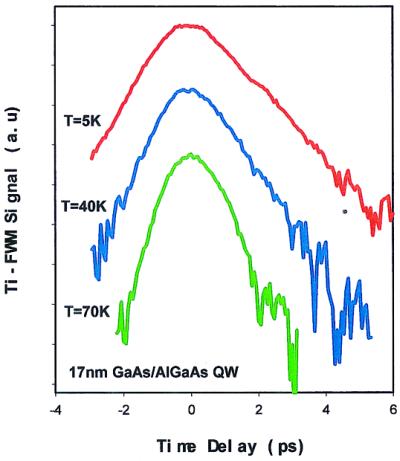
Two-particle correlation effects seen in time-integrated FWM experiments. The strong signal observed at negative time delay, with a rise time exactly half the decay time, is in contradiction with theory for atomic systems and is a signature for Coulomb correlation between electrons and holes (1).
It is interesting to note that in the simplest case of a two parabolic-band semiconductor and under stationary conditions, the semiconductor Bloch equations theory is formally equivalent to the BCS theory of superconductors with an effective Hamiltonian that is the direct analog of Anderson's pseudo-spin Hamiltonian. In the case of laser-excited semiconductors, however, the pairing occurs in the electron-hole channel, the chemical potential is replaced by the photon energy expressing that each electron-hole pair is created by a photon, and the gap equation contains an extra term, the Rabi frequency μ̂⋅E, indicating that the coherence does not appear spontaneously, but is induced by the laser. All of these results stress the profound effects caused by the Coulomb interaction on the optical response of semiconductors, which results in a number of unexpected effects. For example, the semiconductor Bloch equations theory predicted that in contrast with atomic systems the coherent wave mixing emission is in fact delayed. This prediction was verified experimentally, and in the case of high-quality samples delays more than 1 order of magnitude longer than the excitation pulses were observed, with a coherent wave mixing emission appearing as a pulse completely separated from the laser pulse. These experiments show that the physics of semiconductors excited by a laser field is more closely related to that of strongly interacting many-body systems than to that of atoms. Ultrafast nonlinear optical studies of semiconductors therefore provide new insights into the nature of all strongly interacting systems.
Evidence for even higher-order particle correlations was obtained recently. These experiments were performed at moderate magnetic fields in very dilute exciton gases with the same spin for which bonding between excitons is forbidden, and at such large average distance, d ≈10a0, that interactions were expected to be negligible. Explanation of these observations required extension of the coherent wave mixing theory beyond the time-dependent Hartree-Fock approximation of the semiconductor Bloch equations. A magnetic field B∥z⃗, applied to a semiconductor, force electrons, and holes to spiraling along the z⃗-axis, inducing a three-dimensional to one-dimensional transition for the density of states. It also affects the internal structure of excitons by inducing a shrinkage, ∝ , in the (x⃗,y⃗)-plane, but with no important modification along z⃗. Magnetic confinement is expected to significantly distort hydrogenic systems for fields |B⃗|≫Bc where Bc is the field at which the cyclotron radius equals the Bohr radius. For hydrogen atoms Bc ≈104 T, and this regime can be found only at the surface of neutron stars. In the case of a semiconductor such as GaAs where Bc ≈3.4 T, it is easily explored, thus providing a perfect tabletop laboratory for studying many-body interactions between highly distorted hydrogen-like systems. Fig. 4 depicts the STI(Δt) signal from a thin, high-quality GaAs layer with two types of excitons, respectively associated with the light-hole and heavy-hole valence bands, for a series of magnetic fields up to |B⃗| = 10 T ≈3Bc. For Δt>0, STI(Δt) has the expected profile: beats between the two exciton resonances superimposed on a decoherence exponential. This behavior changes only slightly with B⃗. In contrast, the Coulomb-induced signal STI(Δt) for Δt<0 changes drastically as B⃗ increases. Its magnitude increases significantly while its profile becomes highly nonexponential with an unusual positive curvature and extends as far as Δt ≈ −10 ps, or 100 times the laser pulses' duration. The explanation of this effect is that, through the Coulomb interaction between distorted excitons, a coherent four-particle correlation is created in the medium by one of the laser pulses. It corresponds to a two-photon active coherence and, therefore, cannot deliver one photon emission by itself. Thus it is stored in the medium until the second pulse triggers that emission. This coherent memory can be interpreted as a non-Markovian process involving the two-particle correlation polarization waves and interacting with a bath of four-particle correlations. It can be exploited to investigate directly the coherence properties of four-particle correlations, an object rarely accessible to direct measurement.
Figure 4.
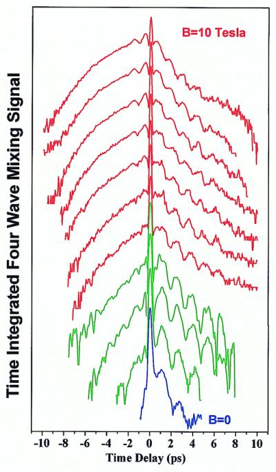
Effects of four-particle correlation revealed by FWM under a large magnetic field. The negative time delay signal increases significantly and its profile becomes highly nonexponential as the magnetic field increases and distort the exciton. This is the signature of a Coulomb-mediated four-particle correlation between excitons (2, 3).
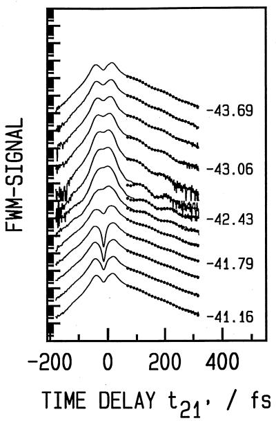
A semiconductor, as any quantum mechanical system, is described by a Schrödinger equation that is local in time. Therefore the knowledge of the Hamiltonian and the present state is enough to determine the future evolution. Thus the classification of a phenomena, coherent or not, as a non-Markovian process nonlocal in time just reflects our inability to solve exactly the many-particle problem for the whole system. In practice we do not know how to solve the time-dependent Schrödinger equation of complex many-body systems, so rather than implementing this ideal program it is customary to divide the total system into a subsystem that we are interested in (for example the interband polarization waves in optics), and the thermal bath of all of the other degrees of freedom on which we have only partial information (in our example the “other carriers” and/or the phonons). At very early times, before scattering processes have randomized the degrees of freedom, the dynamics of the subsystem must have been described by quantum kinetics, with non-Markovian statistics and memory structures (see the discussion above). The main dephasing mechanisms in semiconductors are electron/electron and phonon/electron scattering, including in particular for ionic solids the strong Fröhlich LO-phonon/carrier interaction, which is often the dominant dissipation mechanism. The time scale of the initial phonon/electron non-Markovian regime can be estimated by noting that the time it takes a lattice to react to a perturbation is of the order of one period of its oscillation, i.e., in the case of GaAs, TLO = 115 fs. Indeed non-Markovian effects in the coupling of LO-phonon with interband polarization were observed in GaAs by FWM experiments using ≈14-fs pulses, about eight times shorter than the LO-phonon period. As shown by the 7th-10th curves from the bottom of Fig. 5, the STI(Δt) exhibits a strong oscillatory modulation superimposed on the usual exponential decoherence decay. The period, ≈98 fs, corresponds to the separation between conduction band states coupled by one LO-phonon. These oscillations are not seen in the spectrally resolved signal, which for each Δt consists of a single line without phonon side band, demonstrating that the oscillations seen in the Δt domain are not caused by emission or absorption of phonon but correspond to a coherent memory stored in the LO-phonon bath that affects the interband transition. This phonon/electron process, however, is not irreversible. As any other quantum mechanical “collision” it is an interference with a finite duration. Thus it can be reversed or enhanced, during the duration of the interference by a perturbation whose phase is appropriately chosen. This reversal of a process, which left to itself would become irreversible, was indeed experimentally demonstrated as shown in Fig. 5. The results presented here were obtained by replacing one of the pulses of a canonical coherent wave mixing configuration by a pair of phase-locked pulses 1 and 1′, propagating in the same direction, and separated by the time delay Δt11′ = t1 − t1′ controlled to a precision much smaller than the optical cycle, in this case better than 0.4 fs. This technique, called coherent control, exploits the interference between polarization waves created by the phase-locked fs pulses to control the quantum mechanical excitation pathways of physical and chemical processes and is an exciting area of current research. Fig. 5 shows a series of STI(Δt) plotted vs. the usual Δt, but measured for several values of Δt11′ covering approximately only one optical cycle. Depending on Δt11′, the phonon oscillation seen in the Δt domain can disappear completely (for example, around Δt11′ = −43.64 fs) or can be enhanced (for example, around Δt11′ = −42.38 fs). The detailed theory of these experiments is not yet available, but they demonstrate that by using coherent control of the excitation it is possible to manipulate the so-called irreversible scattering processes.
Figure 5.
Coherent control of phonon/electron interaction. FWM traces obtained by using ≈14-fs phase-locked pulses, about eight times shorter than the LO-phonon period. Depending on the relative phase of these pulses quantum mechanical excitation pathways can be controlled by enhancing or destroying the oscillation induced by electron-phonon interaction (4).
The results discussed in this section, just a few examples selected from a broad body of work obtained over the last decade, demonstrate that by exploiting the time sequence, polarization, and central frequency of ultrashort laser pulses, it is possible to probe the dynamics of many-body interactions in semiconductors with an unprecedented flexibility and accuracy.
Exploiting Envelope Wavefunctions for Probing the Dynamics of Fundamental Quantum Mechanical Processes
A number of fundamental quantum mechanical processes, such as wavepacket motion, tunneling, or Bloch oscillations are rather difficult to observe and investigate in atomic systems or bulk crystals. Semiconductor nanostructures have an inherent advantage for demonstrating and investigating these processes because they can be fabricated to precise specifications. In this section we give a few examples showing how a combination of time-energy rescaling of envelope wavefunctions in custom-made quantum structures (see Box B2) and ultrafast nonlinear optics allows one to not only observe these fundamental quantum mechanical phenomena but also investigate them thoroughly.
One of the most direct manifestations of quantum mechanics is the process of tunneling, by which a particle can “tunnel” through a barrier of energy higher than its own energy. Semiconductor nanostructures such as asymmetric double-quantum well structures (a-DQWS) provide an ideal system for studying this effect and investigating the dynamics of wavepacket oscillations. The a-DQWS consist of two quantum wells of different thickness made of a low energy-gap material, separated by a thin barrier layer of a larger energy-gap material (see Box B2). By the application of an external electric field, an energy level of the conduction band electrons in the narrow well (NW) can be tuned through one of the wide well (WW). When the energy levels are far from one another the electron wavefunctions are localized primarily in one well or the other. As the levels are brought near coincidence the states are delocalized and have nearly equal amplitude in the two wells. The holes, because of their much larger masses, remain localized. An excitation with an ultrashort optical pulse whose spectrum is tuned to the energy of the transition between the WW hole and the electron levels, creates an electronic wavepacket that is a linear superposition of the eigenstates of the a-DQWS. This wavepacket initially is created in the WW but oscillates between the two wells because the two eigenstates have different energies. In other words, the electron tunnels back and forth through the energy barrier with a period determined by the splitting between the electronic levels. Such oscillations were indeed generated and investigated by time-resolved nonlinear optical techniques pump/probe and coherent wave mixing, which are sensitive to the Pauli blocking of the interband transitions, and thus can discriminate when the electron is in the WW. The pump/probe signal has both coherent and incoherent components, whereas the coherent wave mixing is strictly a coherent process so that the associated signal disappears as the coherence of the wavepacket is destroyed. Fig. 6 shows an example of wavepacket oscillations observed by these two techniques in an a-DQWS that consists of a 14-nm GaAs WW and a 10-nm GaAs NW separated by a 2.5 nm thick Al0.35Ga0.65As barrier. The period and initial amplitude of the oscillations can be varied by the external electric field that changes the splitting between the electron levels in the NW and WW. The detailed description of the wavepacket oscillation requires accounting for many-body effects caused by the correlation between the delocalized electrons and the localized holes.
Figure 6.
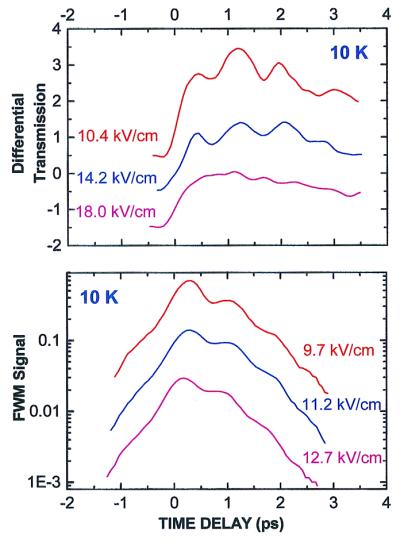
Dynamics of electron wavepacket oscillations in an a-DQWS. The evolution of the amplitude, period, and coherence of the oscillation is observed as the electron tunneling is changed by the applied electric field. (Upper) Pump/probe differential transmission signal and (Lower) coherent FWM signal are plotted as a function of Δt, the time delay between the two pulses (5).
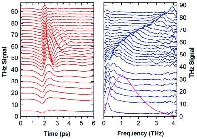
Another interesting feature of these electronic oscillations is that they generate a dipole oscillating with the same period and thus they are a source of THz radiation, which has been observed as shown in Fig. 7 Upper. The frequency spectrum of that radiation (Fig. 7 Lower), shows that the emission results from two distinct mechanisms: (i) an initial transient with a broad spectrum extending from DC to the inverse of the laser pulsewidth, and lasting approximately the duration of these pulses, and (ii) a resonant radiation originating from the oscillating electronic dipole. The resonant radiation was found to be the dominant signal after the detector response was considered. The frequency of the resonant radiation can be varied by changing the electric field.
Figure 7.
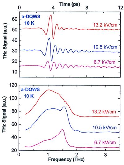
THz radiation emitted by the electronic wavepacket of Fig. 6. (Upper) Time evolution of the coherent emission for various static fields that change the splitting between the electronic level and thus the THz frequency. (Lower) Frequency spectrum showing that the emission results from two physical mechanisms, a broad band initial transient and the radiation of the oscillating electronic dipole (6).
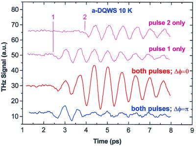
Constructive and destructive interference between eigenstates plays a key role in the wavepacket oscillations. They are a perfect example for applying the technique of coherent control described in the previous section. Fig. 8 shows the results of an experiment in which the THz emission was controlled by varying the relative phase between two phase-locked pulses exciting the sample. Fig. 8 shows the THz waveform emitted under four different conditions. The top two traces show the waveforms when the a-DQWS is excited by only one of the phase-locked pulses. These waveforms are identical except for a delay. When, however, the pair of phase-locked pulses excite the a-DQWS the waveforms show a strong dependence on their relative phase. For Δφ = 0, the two pulses are in phase, there is a constructive interference, and the THz emission is strongly enhanced. In contrast, for Δφ = π the interference is destructive, the THz emission starts at the arrival of the first pulse, but is almost completely quenched by the second one. Recently, experiments have demonstrated coherent control of a number of different aspects of exciton polarization with potentially interesting applications.
Figure 8.
Coherent control of the quantum interference that causes wavepacket oscillations. Upper two traces: THz waveforms seen when the a-DQWS is excited by only one pulse. Lower two traces: Waveforms seen with excitation by a pair of phase-locked pulses. For Δφ = 0, the coherent excitation strongly enhances the THz emission, for Δφ = π, the interference is destructive and the THz emission starts at the arrival of the first pulse, but is almost completely quenched by the second one (7).
In 1928 Bloch proposed that an electron wavepacket in a periodic (crystalline) solid, peaked at a given quasi-momentum, would undergo an oscillation in momentum and real space under an applied electric field. Bloch's proposal assumed that transitions to other energy bands could be neglected. For several decades after this proposal, there was a heated debate in the literature and there was no experimental observation of Bloch's prediction. A major problem in the experimental realization of conditions for observing Bloch oscillations is that their period, τBO = h/eFd, is inversely proportional to the applied field F and to the lattice period d. In general it is possible to observe an oscillating phenomenon only if its period is smaller than its dephasing time. For Bloch oscillations in a crystal the lattice constant is fixed and of the order of a few Å, and there are a variety of uncontrollable dephasing processes. Therefore, the only variable at the experimenter's disposal is the applied electric field, but then one needs electric fields F>1 MV cm−1 to make the oscillation period shorter than the dephasing time. At such high fields, transitions to other bands cannot be ignored and one of Bloch's assumptions fails. One can, however, exploit the change of scale associated with envelope wavefunctions and look for Bloch oscillation in a superlattice (see Box 2). In these artificial quantum structures the period can be tailored to specific values as large as hundreds of Å, i.e., about 2 orders of magnitude larger than the crystal period, and excitonic correlations lengthen dephasing time to the ps range. This brings the Bloch oscillation period for the envelop wavefunction in a range much smaller than the dephasing time for reasonable values of the applied electric field.
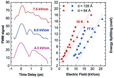
The idea of optically excited Bloch oscillations is a direct extension of the wavepacket oscillations in a-DQWS discussed above. In the case of an a-DQWS, one dealt with only two electronic levels. A superlattice with 2N + 1 periods has a miniband with 2N + 1 unequally spaced eigenstates (see Box B2), the application of an electric field exceeding some critical value converts these miniband states into 2N + 1 equally spaced Wannier levels. Optical excitation with an ultrashort pulse creates a wavepacket made up of superposition of these eigenstates. The dynamics of this wavepacket is quite complicated and depend on many factors including correlation effects and spectral overlap. Nevertheless, one expects it to undergo oscillations at the Bloch period τBO and weaker ones at its harmonics. As for the a-DQWs these oscillations can be triggered by optical excitation and their dynamics followed by time-resolved nonlinear optical spectroscopy. Indeed, nearly 60 years after the proposal, the existence of Bloch oscillations was demonstrated in semiconductor superlattices. This is shown in Fig. 9 Left, which depicts the FWM signal from a superlattice consisting of 40 periods each formed by a 10-nm GaAs quantum well and a 1.7-nm Al0.3Ga0.7As barrier. The characteristic oscillations of the FWM signal follow the Bloch formula τBO = h/eFd and agrees with splitting of the superlattice levels, i.e., the Wannier-Stark ladder as shown in Fig. 9 Right.
Figure 9.
Signature of Bloch oscillations in a superlattice. (Left) FWM signal measured from a 40-period superlattice. The oscillations of the FWM signal follow the Bloch formula τBO = h/eFd. (Right) Variation of the Bloch oscillation frequency h/τBO, of two superlattices, d = 12.8 nm and d = 8.4 nm, as a function of the applied electric field F and for two temperatures (8).
The motion of the electron wavepacket in the Bloch oscillations can be quite complicated because of the correlation effects between the localized holes and the delocalized electrons and depends critically on the central frequency of the exciting laser pulse. This motion can evolve between two extremes, a symmetric breathing mode, where the center of mass of the electrons does not move, and an asymmetric swinging mode, where that center of mass undergoes large oscillations. In the first case there is no induced radiating dipole, whereas the swinging mode radiates at a THz frequency νBO = 1/τBO. Fig. 10 shows the THz emission observed on a 35-period GaAs/Al0.3Ga0.7As superlattice with a 9.7-nm quantum well and 1.7-nm barrier. Fig. 10 Left shows the amplitude of the THz waveform emitted by the superlattice for various applied bias voltages. As the electric field increases, the waveform develops a distinct oscillatory behavior, demonstrating the existence of an oscillating dipole in the superlattice. The oscillation frequency increases with the electric field, as shown in the spectrum of the emitted radiation presented in Fig. 10 Right. Other type of experiments have shown that the amplitude of the electron center of mass motion is indeed very large, i.e., ≈1.4 nm. Note that some experiments have demonstrated that Bloch oscillations persist to room temperature under certain conditions. Because νBO ≈4 THz this may have an immense practical interest. Finally, it is worth noting that a totally different system, atoms moving in an accelerating optical lattice, also has exhibited Bloch oscillations.
Figure 10.
THz emission of a 35-period superlattice. (Left) The amplitude of the THz waveform emitted for various applied bias voltages. (Right) As the electric field increases, the waveform develops a distinct oscillatory behavior demonstrating the existence of an oscillating dipole (9).
Conclusion
We have presented highlights of recent results in the ultrafast nonlinear optics of semiconductors and their nanostructures. We have stressed that the difference in the energy, time, and length scales of the envelope wavefunction of quasi-particles in semiconductors compared with those in the atomic systems makes it possible to explore properties and phenomena not accessible under ordinary conditions in other systems. This property of semiconductors, along with the ability to custom-design high-quality nanostructures, has been exploited in recent years to gain insights into such diverse phenomena as many-body effects, quantum kinetics, and wavepacket oscillations resulting from the most fundamental quantum mechanical properties of the system. These investigations have been achieved by using ultrashort laser pulses and nonlinear optical techniques. The results show that many-body interactions make semiconductors more like a strongly interacting system than an atomic system and also demonstrate the effects of higher-order correlations, quantum kinetics, and reversibility of quantum collisions. They further demonstrate the most fundamental quantum mechanical phenomena of tunneling and wavepacket oscillations. These results provide new insights not only into the nature of semiconductors but also other condensed matter systems where such phenomena are not experimentally accessible.
General References
Because of the volume of published work in this field we give here only a short list of general reviews.
Haug, H. & Koch, S. W. (1993) Quantum Theory of the Optical and Electronic Properties of Semiconductors (World Scientific, Singapore), 2nd Ed.
Mukamel, S. (1995) Principles of Nonlinear Optical Spectroscopy (Oxford, New York).
Shah, J. (1999) Ultrafast Spectroscopy of Semiconductors and Semiconductor Nanostructures (Springer, Berlin), 2nd Ed.
Haug, H. & Jauho, J.-P. (1996) Quantum Kinetics in Transport and Optics of Semiconductors (Springer, Berlin).
Chemla, D. S. (1999) in Ultrafast Transient Nonlinear Optical Processes in Semiconductors in Nonlinear Optics in Semiconductors, eds. Willardson, R. K. & Weber, E. R. (Academic, New York), pp. 175–256.
Schäfer, W. & Wegener, W. (1999) Semiconductor Optics and Transport Phenomena (Springer, Berlin).
Figure 2.
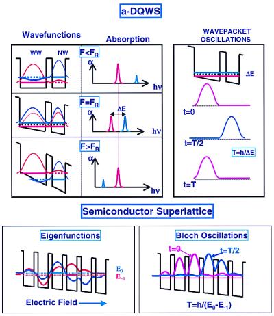
(Upper) Schematic representation of the energy levels, wavefunctions, and wavepacket oscillations in a-DQWS. (Left) a-DQWS for three different bias values; FR is the field at which the two lowest electron levels are in resonance. The schematic absorption spectra are shown on the right. (Right) Wavepacket oscillations when a spectrally broad ultrashort pulse excited the wavepacket in the WW. (Lower) Semiconductor superlattice. (Left) Schematic diagram of the two lowest electron energy levels and their eigenfunctions. (Right) Bloch oscillations in the superlattice when the wavepacket is initially excited in well 0, the third well from the left.
Acknowledgments
D.S.C.'s work was supported by the Director, Office of Energy Research, Office of Basic Energy Sciences, Division of Material Sciences of the U.S. Department of Energy, under Contract No. DE-AC03–76SF00098.
Abbreviations
- GaAs
gallium arsenide
- FWM
four-wave mixing
- a-DQWS
asymmetric double-quantum well structure
- NW
narrow well
- WW
wide well
- LO
longitudinal optical.
Footnotes
This contribution is part of the special series of Inaugural Articles by members of the National Academy of Sciences elected on April 29, 1997
Specific References
- 1.Leo K, Wegener M, Shah J, Chemla D S, Gobel E O, Damen T C, Schmitt-Rink S, Schäfer W. Phys Rev Lett. 1990;65:1340. doi: 10.1103/PhysRevLett.65.1340. [DOI] [PubMed] [Google Scholar]
- 2.Kner P, Bar-Ad S, Marquezini M V, Schafer W, Chemla D S. Phys Rev Lett. 1997;78:1319–1322. doi: 10.1103/PhysRevLett.77.3177. [DOI] [PubMed] [Google Scholar]
- 3.Kner P, Bar-Ad S, Marquezini M V, Chemla D S, Lövenich R, Schäfer W. Phys Rev B. 1999;60:4731–4748. [Google Scholar]
- 4.Wehner M U, Ulm M H, Chemla D S, Wegener M. Phys Rev Lett. 1998;80:1992–1995. [Google Scholar]
- 5.Leo K, Shah J, Göbel E O, Damen T C, Schmitt-Rink S, Schäfer W, Köhler K. Phys Rev Lett. 1991;66:201–205. doi: 10.1103/PhysRevLett.66.201. [DOI] [PubMed] [Google Scholar]
- 6.Roskos H G, Nuss M C, Shah K, Leo K, Miller D A B, Fox A M, Schmitt-Rink S, Köhler K. Phys Rev Lett. 1992;68:2216–2220. doi: 10.1103/PhysRevLett.68.2216. [DOI] [PubMed] [Google Scholar]
- 7.Planken P C M, Brener I, Nuss M C, Luo M S C, Chuang S L. Phys Rev B. 1992;48:4903–4906. doi: 10.1103/physrevb.48.4903. [DOI] [PubMed] [Google Scholar]
- 8.Leo K, Haring-Bolivar O, Brüggemann F, Schwedler R. Solid State Commun. 1992;84:943–946. [Google Scholar]
- 9.Waschke C, Roskos H G, Schwedler R, Leo K, Kurz H, Köhler K. Phys Rev Lett. 1993;70:3319–3323. doi: 10.1103/PhysRevLett.70.3319. [DOI] [PubMed] [Google Scholar]


