Abstract
We demonstrate the use of self-assembly for the integration of freestanding micrometer-scale components, including single-crystal, silicon field-effect transistors (FETs) and diffusion resistors, onto flexible plastic substrates. Preferential self-assembly of multiple microcomponent types onto a common platform is achieved through complementary shape recognition and aided by capillary, fluidic, and gravitational forces. We outline a microfabrication process that yields single-crystal, silicon FETs in a freestanding, powder-like collection for use with self-assembly. Demonstrations of self-assembled FETs on plastic include logic inverters and measured electron mobility of 592 cm2/V-s. Finally, we extend the self-assembly process to substrates each containing 10,000 binding sites and realize 97% self-assembly yield within 25 min for 100-μm-sized elements. High-yield self-assembly of micrometer-scale functional devices as outlined here provides a powerful approach for production of macroelectronic systems.
Keywords: macroelectronics, plastic electronics, self-assembly
Macroelectronics is an emerging area of interest in the semiconductor industry. Unlike the traditional pursuit in microelectronics to build smaller devices and achieve higher degrees of integration over small areas, macroelectronics aims to construct distributed active systems that cover large areas. Often, these systems are constructed on flexible substrates with multiple types of components and allow for distributed sensing and control. A number of applications are already under consideration for macroelectronics, including smart artificial skins (1), large-area phased-array radars (2), solar sails (3), flexible displays (4, 5), electronic paper (4), and distributed x-ray imagers (6). A candidate macrofabrication technology must be able integrate a large number of various functional components over areas exceeding the size of a typical semiconductor wafer in a cost-effective and time-efficient fashion.
The substrate of choice for many macroelectronic applications is plastic. Flexible plastic substrates are thermally and chemically incompatible with conventional semiconductor fabrication processes. To incorporate electronic devices, a number of venues have been explored for low-temperature integration of semiconductors on plastics. The integration of semiconductor is followed by steps to build and interconnect functional devices. These material integration methods have demonstrated functional devices on plastic built from amorphous silicon (7), low-temperature polysilicon (8), and organic semiconductors (9, 10). Although in some applications low-performance devices are acceptable, in many applications, such as phased-array radar antennas or radio frequency tags, the integrated devices are required to perform at high frequencies with low power consumption. Devices built with the material integration methods outlined above suffer from low charge carrier mobility. Typical amorphous silicon transistors have electron mobility of 1 cm2/V-s (11), low-temperature polysilicon transistors on plastic have electron mobility of ≈65 cm2/V-s (8), and organic semiconductor transistors demonstrate charge carrier mobility of ≈1 cm2/V-s or much lower (12, 13). Poor charge carrier mobility in these devices [in comparison, the electron mobility in single-crystal silicon transistors exceeds 1,000 cm2/V-s (14)] translates to poor frequency response and high power consumption. Some of the best devices demonstrated to date were made by means of a creative approach that uses silicon ribbons released from a wafer and reassembled on a polymer substrate to yield stretchable circuits (15, 16). This method has produced circuits with form factors replicating the original silicon wafer (the area and coverage attained are similar to a wafer originally used for processing) and with performance parameters that are affected by strain applied to the substrate. The approach has demonstrated electron mobility as high as 100 cm2/V-s, which remains short of the performance offered by transistors fabricated in single-crystal silicon.
An alternative approach for the construction of macroelectronic systems is to perform the integration at the device instead of the material level (17). Significant infrastructure is available to cost-effectively fabricate high-performance devices on single-crystal semiconductor substrates. These devices can be released and reassembled on a large-area plastic substrate. Recent advances in robotic assembly (18) allow for positioning of up to 26,000 components per hour on plastic substrates; however, the relatively moderate speed, high cost, and limited positional accuracy of these systems make them unsuitable candidates for cost-effective mass production of macroelectronics. For component sizes of <200–300 μm, robotic assembly techniques become exceedingly slow because of the delay in the control mechanisms necessary to position parts with high accuracy and the need to overcome parasitic stiction forces (18). A conservative estimate puts the assembly cost with a state-of-the-art robotic pick-and-place system at ≈0.7 cents per component (19). At this rate, assembly of large-area systems with thousands to millions of components becomes too costly for most applications.
A powerful technology that can meet all of the criteria for an effective macrofabrication technology is self-assembly. In a device-level integration approach based on self-assembly, functional devices are batch-microfabricated and released to yield a freestanding collection. These components are then allowed to self-assemble onto a template, for example on a plastic substrate, to yield a functional macroelectronic system. Used in this fashion, self-assembly is an inherently parallel construction method that allows for cost-effective and fast integration of a large number of functional components onto unconventional substrates (19). The key components of a self-assembly-based macroelectronic fabrication technology are (i) development of fabrication processes that generate freestanding micrometer-scale functional components, (ii) implementation of recognition/binding capabilities that guide the self-assembly of components in the correct location, and (iii) determination of self-assembly procedures that construct the final system with a high yield.
Self-assembly of micrometer- and millimeter-scale components has been studied previously both for 2D (20–24) and 3D integration (25, 26). In 2D integration via self-assembly, a template with binding sites is prepared, and a collection of parts is allowed to self-assemble onto the proper binding sites in a liquid medium. Capillary forces are used to bind the components to the template, and forces resultant from fluid flow and gravity are used to move the components and drive the system toward a minimum energy state (20, 22). A major drawback of demonstrated self-assembly to this date has been the requirement for postprocessing. In all of these demonstrations, further processing of the substrate in a cleanroom has been necessary to provide electrical connections and complete the assembly procedure. The need for postprocessing limits the applicability of these demonstrations when access to large areas and cost-effectiveness are critical factors. An alternative two-step approach relies on capillary forces of hexadecane for the primary alignment and then the capillary forces of a molten alloy to create the mechanical and electrical connections for placement of high-quality inductors (27). Self-assembly has also been used for 3D integration of freestanding millimeter-scale parts or folding of components placed on ribbons into electrical circuits (25). These pioneering works have provided the inspiration for further development of self-assembly as a method of manufacturing heterogeneous systems. For the full potential of these techniques to be realized, batch microfabrication processes are needed to generate a large number of micrometer-scale functional components that can participate in self-assembly.
In this article, we present a method to batch-fabricate micrometer-scale functional devices, such as silicon field-effect transistors (FETs), that can participate in a self-assembly process. The self-assembly is performed in a fluid environment in a single step, removing the need for postprocessing and allowing for the integration of microcomponents over large areas. The self-assembly process is programmed by matching shapes between the microcomponents and the target template. Capillary forces resultant from a molten alloy are used to bind the microcomponents to the target location, and fluid-flow forces and gravity are used to transport the microcomponents and guide the system toward a minimum energy state. Three main demonstrations of the self-assembly technique are presented: (i) the assembly of multiple shapes of microcomponents onto a common substrate, (ii) the self-assembly of single-crystal silicon FETs and diffusion resistors to create high-performance electronic circuitry on plastic substrates, and (iii) the rapid and high-yield self-assembly of up to 10,000 silicon microcomponents onto a plastic template. Through these demonstrations, the self-assembly technique is verified to be extendible to multiple types of microcomponents, to be able to integrate high-performance, active circuitry on plastic in a single step, and to be massively parallel and suitable for manufacturing.
Overview of the Self-Assembly Process
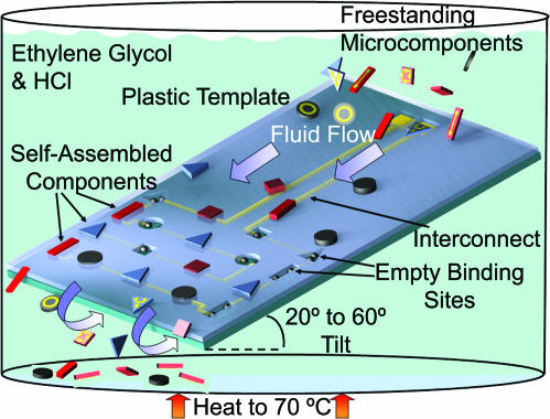
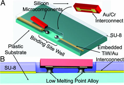
The assembly process is illustrated in Figs. 1 and 2. We first fabricated silicon microcomponents on a silicon wafer and then released them to yield a collection of freestanding microcomponents resembling fine powder. Each of the microcomponents carried metal contacts and had a specifically defined shape. Separately, we prepared plastic templates with embedded metal interconnects and binding sites with various shapes made of polymer. At the bottom of the binding sites, we positioned areas covered by an alloy with a low melting point. The self-assembly process involved submerging both the silicon microcomponents and the plastic template into a fluid and agitating to induce movement of the microcomponents over the substrate. When the shape of a microcomponent and the corresponding well matched, the microcomponent fell into the well allowing contact between the molten alloy at the bottom of the well and the metal pads positioned on the surface of the microcomponent. The resultant capillary force kept the microcomponent in the well preventing the fluid flow to dislodge the bound part. If the component entered the well upside-down, a capillary connection could not be made and fluid forces forced the component out of the well. After the completion of the self-assembly process, the temperature was lowered to solidify the molten alloy and to make the mechanical and electrical connections between the microcomponents and the template permanent.
Fig. 1.
The heterogeneous self-assembly process. Microcomponents are introduced over a template submerged in a liquid medium and moved with the fluid flow. Self-assembly occurs as microcomponents first fall into complementarily shaped wells and then become bound by the capillary forces resultant from a molten alloy.
Fig. 2.
Details of the self-assembly process for a single microcomponent. (A) The microcomponent approaches a binding site with complementary shape. (B) The microcomponent is held by capillary force resultant from molten-alloy-bridging the metal pads positioned on the microcomponent and on the template.
We performed three types of experiments to test the self-assembly technique. First, we fabricated passive silicon microcomponents (referred to as silicon elements) with prescribed shapes and containing only metal interconnections (refer to Fig. 2) to investigate the use of shape recognition to integrate multiple types of microcomponents onto a common substrate. In this manner, successful assembly was verified when the assembled elements completed an embedded electrical network on a plastic substrate. Second, we developed freestanding n-type FETs to test the use of self-assembly to create active electronic circuitry with silicon FETs embedded in plastic substrates. Finally, we tested the self-assembly of circular silicon elements onto templates each containing 10,000 binding sites to determine the yield and rate of the self-assembly process. For this experiment, we used only circular elements because this shape demonstrates the fastest self-assembly and consistently attains high assembly yield (28).
Design and Fabrication of the Microcomponents and the Plastic Templates.
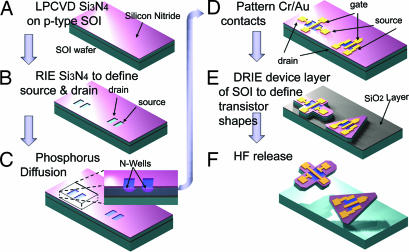
Silicon elements and the n-type FETs were fabricated on and released from a silicon-on-insulator (SOI) wafer. Both microcomponent types were constructed in a similar fabrication process that is based on (i) metallization to create Cr/Au contact pads, (ii) geometric shape definition through deep reactive ion etching, and (iii) microcomponent release from the SOI wafer by wet etching the buried silicon dioxide layer. The fabrication of the FETs contains additional steps as delineated in Materials and Methods and shown in Fig. 3. Fabrication of the transistors was unusual, however, because we used Si3N4 both as a diffusion mask and as the gate dielectric layer. Silicon dioxide is the standard gate dielectric in most FETs, but the hydrofluoric acid used to release the components in our process would readily etch a silicon dioxide dielectric layer. Therefore, we used a low-pressure, chemical-vapor-deposited, low-stress Si3N4 to serve as the gate dielectric layer and the mask during phosphorus diffusions (Fig. 3A).
Fig. 3.
Transistor microfabrication process flow. Completion of the last step yields a collection of micrometer-scale, released components.
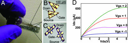
We chose four mutually exclusive (one shape cannot assemble in another shape's binding site) element geometries (circles, rectangles, squares, and triangles), because they present different levels of symmetry. Symmetric elements assemble faster and with a higher yield; however, elements with asymmetric structure offer a higher degree of control over the final configuration of the self-assembled structure. We used circular elements for high-yield self-assembly experiments and triangular components for self-assembly of FETs to ensure the proper electrical contact with the three terminals of the transistors. The dimensions of the microcomponents varied depending on the particular shape, ranging from 100 μm (circle diameter) to 300 μm (rectangle length). For all shapes, the microcomponent thickness ranged from 10 to 20 μm, according to the device layer thickness of the SOI wafer used for fabrication. The metal contact pad dimensions were 50 × 50 μm for the elements and 40 × 40 μm for the FETs and diffusion resistors. Fig. 4 shows the FETs after release from the SOI wafer. The measured transistor performance of the triangular FETs is shown in Fig. 4D. The fabrication process of the plastic templates is illustrated in Fig. 5 and described in detail in Materials and Methods.
Fig. 4.
Released silicon FETs. (A) A collection of freestanding single-crystal silicon FETs. (B and C) Optical microscope images of and triangle-shaped (B) cross-shaped (C). (D) Measured performance of a typical triangular transistor before release from SOI wafer.
Fig. 5.
Plastic template fabrication flow.
The Self-Assembly Procedure.
To prepare the components for self-assembly, we cleaned them with a short piranha etch [3:1 (vol/vol) H2SO4/H2O2] to ensure that the metal contacts were contaminant-free. To make certain the solder pads on the substrate were clean, we performed the alloy dip-coat immediately before use for self-assembly. After the dip-coat process, we positioned the substrate on an angled glass slide (20–60°) and immersed it into neat ethylene glycol serving as the self-assembly medium.
To perform the self-assembly, we first heated the ethylene glycol solution to 70°C to melt the alloy within the binding sites and to decrease the viscosity of the ethylene glycol to allow for better motion of the microcomponents through the fluid. Next, we lowered the solution pH to 3.0 with the addition of HCl to clean surface oxides forming on the molten alloy. We manually introduced a collection of microcomponents (using only one microcomponent shape at a time) directly above the substrate binding sites. Typically, we introduced 10–100 times more microcomponents than the number of available binding sites to increase the likelihood of self-assembly. The microcomponents were allowed to flow over the template and self-assemble upon an encounter with a complementarily shaped binding site (refer to Fig. 1). Once all available microcomponents had passed over the substrate (one microcomponent pass), we initiated the process again by collecting and manually reintroducing microcomponents over the substrate. We repeated this process until all available binding sites contained a self-assembled microcomponent, which typically occurred after five microcomponent passes (refer to High-Yield Self-Assembly in Results and Discussion).
We provided a constant fluid motion with a pipette and positioned the self-assembly medium over a shaker table (set to provide gentle vibrations at 20 Hz) to provide extra external agitation. Ideally, the agitation should induce microcomponent movement across the substrate, break-up microcomponent aggregations, and disassemble incorrectly assembled microcomponents while allowing the correctly assembled microcomponents to remain in place. We found that a laminar fluid flow 5–10 cm/s across the substrate was sufficient to break up aggregations or wash them off of the substrate but gentle enough not to disturb correctly self-assembled microcomponents. After the completion of the self-assembly process, we lowered the temperature of the ethylene glycol solution to room temperature to solidify the alloy and make the connections permanent. We then removed the template from the solution for further testing and measurement. We found that long exposure to low pH at elevated temperatures adversely affected the adhesion of the SU-8 polymer layer defining the binding site geometry to the plastic substrate. An alternative method to perform the self-assembly process was to avoid the addition of acid to the self-assembly medium and rely primarily on geometric shape matching to complete the template. After the completion of the shape-matching step, hydrochloric acid was added to break the alloy surface oxide and make the surface available for bonding. The self-assembly medium temperature was then raised for 1–2 min to 90°C to form the capillary bonds between the microcomponents and the template. Subsequent lowering of the temperature yielded permanent mechanical and electrical connections between the microcomponents and the templates.
Results and Discussion
Heterogeneous Self-Assembly of Silicon Elements.
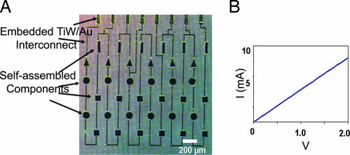
Fig. 6 shows the result of a typical heterogeneous self-assembly procedure. As shown, shape recognition between elements and binding sites allowed for the assembly of different types of elements on a common plastic template. Fig. 6B shows the measured current–voltage curve through two ports of the self-assembled electrical network, demonstrating a low contact resistance of 40 Ω between each element and the embedded interconnection on the template. Differences between the assembly rates of different element shapes were noticeable. Many of the differences can be attributed to element mobility across the substrate. Element–element entanglement and incorrect element–substrate binding were more pronounced for squares and triangles. In general, elements with sharp edges have a higher chance of entanglement; in addition, elements with narrow or high-aspect-ratio regions have a higher chance of entering binding sites incorrectly. The direction of the fluid flow also aided in the alignment of the rectangular elements with the binding sites.
Fig. 6.
Heterogeneous self-assembly results. (A) Optical microscope image of multiple types of microcomponents self-assembled on plastic to complete an electrical network. (B) Measured current–voltage curve between the two leftmost ports of the network verifying proper electrical connection between the microcomponents and the template.
Self-Assembly of FETs.
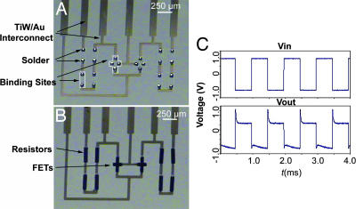
Fig. 7 shows optical microscope images of a plastic substrate before (Fig. 7A) and after (Fig. 7B) self-assembly of FETs and diffusion resistors to create a logic inverter gate employing two n-type FETs in parallel. Fig. 7A shows the alloy dots in the binding sites defined by the transparent SU-8 wells. Fig. 7C shows the measured self-assembled inverter performance (input and output voltages). The electron mobility of the FETs, as measured on plastic, was 592 cm2/V-s, with a source resistance of 218 Ω.
Fig. 7.
Self-assembly of FETs. (A) Optical microscope image of a plastic substrate with empty binding sites (two outlined with white lines for clarity). (B) The template after completion of the self-assembly process showing the position of FETs and diffusion resistors. (C) Measured performance of the inverter shown in B. The overshoot is likely due to the parasitic line capacitance of the interconnection on the substrate.
High-Yield Self-Assembly.
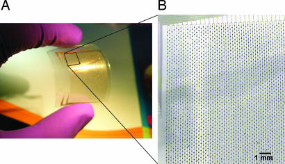
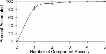
Fig. 8 shows the results of the self-assembly of circular elements onto a template with 10,000 binding sites. A self-assembly yield of >97% was reproducibly achieved across the substrate. Because the self-assembly process is not yet automated [as in ref. 23], the process involved the manual introduction of elements onto the substrate, followed by agitation to pass the elements across the binding sites. After the completion of each pass resulting in either the bonding of the elements to the template or their fall to the bottom of the self-assembly vessel, the unbound elements were collected and reintroduced on the template. This procedure was repeated five times for each template to achieve high-yield self-assembly. To quantify the likelihood of proper binding in the self-assembly process, we performed additional experiments with substrates containing only 600 binding sites and circular elements. Starting with completely empty binding sites (0% self-assembled), we introduced a large number of elements (an order of magnitude more than the number of binding sites) over the substrate and measured the self-assembly yield after all of the excess elements had fallen off the template (one element pass completed). We continued this procedure, each time passing approximately the same number of elements over the substrate. After each pass, we recorded the assembly yield, defined as the number of correctly assembled elements divided by the total number of binding sites on the template. As shown in Fig. 9, >80% of the binding sites were occupied after the first pass; after five passes, nearly all 600 binding sites were filled. The time taken for each element pass was 5 min. We carried out experiments with large numbers of similar elements and binding sites primarily to study the rate and the yield of the self-assembly process in a statistically meaningful fashion; however, it should be noted that the assembly of a large collection of similar elements is of use in applications such as the construction of flexible displays.
Fig. 8.
High yield (≈97%) self-assembly of 100-μm, circular, single-crystal silicon elements onto a flexible plastic template containing 10,000 binding sites. (A) Completed template. (B) Close-up image of ≈2,000 binding sites, self-assembled elements, and electrical interconnects.
Fig. 9.
Measured self-assembly rate. The percentage of correctly self-assembled elements after each element pass step is shown, indicating a 99% average self-assembly yield after five element passes. Error bars indicate the standard deviation.
Surface Energy Modeling.
At the heart of the self-assembly process is the reliance on energy minimization to guide the microcomponents; therefore, we developed finite element models to examine the role of both capillary and fluidic forces on a microcomponent as it self-assembles into a binding site. To model the fluidic forces, we developed a finite element simulation model by using FEMLAB to solve the incompressible Navier–Stokes equation for a constant fluid flow of ethylene glycol across the template in presence of microcomponents. Details of this model are provided elsewhere (29). For this model we assumed a steady-state, laminar flow of 5–10 cm/s across the substrate and a dynamic viscosity of 0.005 Pa-s for ethylene glycol at 70°C. To determine the capillary force acting on the microcomponents as they minimize their free surface energy and become bound in the well, we used the modeling program Surface Evolver (30). The model consisted of two fixed elements: the microcomponent and the template, both containing metallic pads wettable by the molten alloy. The extent of wettability between the alloy and the metal pads is determined by the contact angle, which we experimentally measured to be 30° (low-melting-point alloy on Au while immersed under ethylene glycol at 70°C; refer to Fig. 10B Inset).
Fig. 10.
Modeling results. (A) Calculated energy landscape of component as it joins with solder. (B) Surface Evolver model of capillary forces of molten solder. (Inset) An optical microscope image used to determine the contact angle of molten alloy on gold under ethylene glycol. (C) Capillary forces in the z direction.
Fig. 10 shows the calculated energy landscape (as determined by Surface Evolver) for different spatial configurations as a microcomponent self-assembles. With our particular configuration, the capillary forces were calculated to be in the range of a few hundred micronewtons, whereas the fluidic forces were much smaller, at 2.0–2.5 nN (30). These results indicate that once the microcomponent has self-assembled and established a firm bond to the substrate via the molten alloy, the fluid force alone cannot cause disassembly.
Conclusions
Self-assembly provides a powerful tool for the production of macroelectronic systems. We have demonstrated that microfabrication processes can be developed to make functional microcomponents, such as single-crystal silicon FETs in a powder-like collection and that this collection of microcomponents can be self-assembled onto a flexible plastic template in a single step to yield functional circuitry. The method allows for the integration of microcomponents that are made independently in potentially incompatible microfabrication processes. We have demonstrated functional devices and circuits on plastic substrates with measured electron mobility exceeding 590 cm2/V-s, constituting almost an order of magnitude improvement over the prior state of the art in measured charge carrier mobility of semiconductor devices operating on plastic. Furthermore, there is significant room for improvement in electrical performance of the self-assembled systems. For example, the microcomponent-to-substrate contact resistance of 40 Ω can be decreased by using bismuth-free alloys that are less prone to oxidation. The fairly large FET source resistance, due to a lightly doped region under the gate nitride not covered by the gate metal, can be reduced by using an aligner tool with higher accuracy.
More importantly, we show that self-assembly can provide very high yields of >97%. Although the self-assembly experiments demonstrated here were performed in a laboratory with minimal equipment and manual introduction of parts, the self-assembly rate of 10,000 per 25 min for 100-μm microcomponents rivals the assembly rate of the fastest multimillion dollar robotic assemblers (18). The self-assembly rate can be improved by orders of magnitude via automation of the set-up.
We relied on a shape-matching effect to control the binding locations of multiple microcomponent types on the template and used capillary forces to make connections between the microcomponents and the templates. Both of these effects are scaleable down to the nanoscale should the need arise. Examples of shape recognition for self-assembly (such as in antigen–antibody binding) and capillary-force-driven self-assembly (such as in cell membrane formation) are abundant in nature. Energy minimization driven by gravity is not expected to scale well to the submicrometer region, however, and other binding mechanisms based on charge or hydrogen binding are more appropriate in this regime.
In our demonstrations, we incorporated single FETs or single diffusion resistors in the microcomponents to construct circuits on plastic. In many macroelectronic applications, more complex microcomponents, each perhaps carrying tens of interconnected transistors, may be needed. The microfabrication processes outlined here can be easily modified to accommodate this need. The appropriate level of complexity for each microcomponent for a given application is yet to be determined. Although we made the templates with standard microfabrication techniques, it should be noted that all of the critical dimensions are in the microcomponent structures and not in the template. Once the microcomponents are made and released to form a powder-like collection, the templates can be produced with a variety of techniques that are suitable for large-area patterning. We believe, as verified by the demonstrations provided here, that self-assembly offers an extremely promising venue for construction of the large-area, high-performance macroelectronic systems of the future.
Materials and Methods
Fabrication of Microcomponents.
To fabricate the FETs, we first cleaned the 10- to 20-μm-thick SOI wafers (〈100〉 p-type, 1–10 Ω-cm device layers and 0.5- to 1-μm-thick buried silicon dioxide layers) with a 5-min piranha etch [3:1 (vol/vol) H2SO4/H2O2] followed by a 1-min buffered oxide etch (BOE) to strip the native oxide. Next, the wafers were cleaned for 5 min in 1:1:5 ammonium hydroxide/H2O2/H2O, followed by 5 min in 1:1:5 HCl949H2O2/H2O, at 70°C. Next, we deposited 200 nm of Si3N4 using low-pressure, chemical vapor deposition. The next step was to pattern the nitride to define the n-well areas of the transistor. After patterning the photoresist AZ1512 (Microchem, Newton, MA) and baking the resist for 5 min at 110°C, we etched the nitride using reactive ion etching (50 standard cm3/min of SF6 at 250 mTorr and 100 W for 100 s) to expose the underlying p-type silicon (Fig. 3B). We removed the photoresist with acetone and repeated the cleaning procedure described above to prepare the wafers for doping. We used spin-on phosphorus dopant glass (catalog no. P-8545; Honeywell, Tempe, AZ) and a drive-in at 950°C for 30 min to achieve a junction depth of 0.9 μm (Fig. 3C). After diffusion, we removed the dopant glass with a 1:10 BOE. Next, we performed a low-temperature (850°C) dry oxidation and anneal for 30 min on the wafers and stripped all of the remaining silicon dioxide with BOE. To create the source, drain, and gate contacts, we first patterned a photoresist AZ4620 (target, 6 μm) and performed an oxygen plasma clean at 300 W for 1 min. By using an electron-beam evaporator, we deposited 10 nm of Cr followed by 400 nm of Au. After evaporation, the metal pads were defined by sonication and lift-off in acetone (Fig. 3D). With an additional photoresist-patterning step using AZ4620 coating, we defined the transistor microcomponent shapes first by using reactive ion etching through the nitride layer and second by using a deep reactive ion etch through the device layer of the SOI wafer down to the buried oxide (Fig. 3E). We then removed the photoresist with acetone and released the transistors by immersing the wafer in a 49% hydrofluoric acid bath for 20 min. Exposure to hydrofluoric acid removed the buried silicon dioxide layer and released the microcomponents into the solution. We isolated, rinsed, and stored the powder-like collection of released microcomponents in deionized water (Fig. 3F). We used a similar fabrication process to make the diffusion resistor by taking advantage of the phosphorous diffusion region to form the resistive path. We fabricated the freestanding silicon elements in a similar but much simplified process, because they required only metallization, geometric shape definition, and hydrofluoric acid release.
Fabrication of the Plastic Templates.
To prepare the templates, we used 8.5- × 11-inch (1 inch = 2.54 cm) sheets of thermally stable, 100-μm-thick polyester (part no. LT04_08_5_11_100S; Policrom, DriveBensalem, PA) cut into the shape of a 4-inch wafer. We chose this plastic because it is clear, flexible, can withstand temperatures of up to 80°C without significantly warping, and is compatible with the developer used for photolithography (AZ400K; Microchem). We thoroughly rinsed the substrate with acetone and isopropyl alcohol to remove any contaminants and patterned it by using photolithography (AZ460, target thickness, 6 μm) as shown in Fig. 5B. We followed the photoresist patterning by sputtering TiW/Au (10 nm/200 nm) on the substrate performed at low power (50 W; deposition rate, 10 nm/min) to prevent heat-induced warping of the plastic wafer. After the sputter deposition, we performed a lift-off process by stripping the remaining photoresistant coating with acetone and a brief sonication to define the metal interconnects on the wafer (Fig. 5C). To shape the binding sites with the desired geometry and depth (10–20 μm), we used a clear, cross-linkable negative photoresist, SU-8. The binding-site wells were designed to accommodate a microcomponent with a complementary shape and express a flat surface after the completion of the self-assembly process. To prepare the wafer for SU-8 deposition, we thoroughly rinsed the wafer with isopropyl alcohol and baked it at 60°C for 5 min. The SU-8 layer was formed by spinning SU-8 2015 (Microchem) at 3,000 rpm (Photoresist spin coater 100 from CEE) for 30 s to give an average thickness of 15 μm followed by exposure and development. To prevent heat-induced warping of the wafer, we modified the hard bake and postexposure bake from the Microchem specifications to be 60°C for 10 min each. After SU-8 patterning, the only metal areas exposed were contact pads (30 × 30 μm) centered at the bottom of the SU-8 wells (Fig. 5D). We used dip-coating in a low-melting-point alloy, 44.7% Bi/22.6% Pb/19.1% In/8.3% Sn/5.3% Cd (melting point, 47°C; part no. LMA-117 from Small Parts, Inc., Miami Lakes, FL), which was pooled to dewet the alloy on the exposed metal pads (Fig. 5E) and complete the template fabrication process.
Acknowledgments
We thank the staff of the microfabrication facility at the Washington Technology Center for help with cleanroom processing. This work was supported by Defense Advanced Research Projects Agency Grant FA9550-04-1-0257.
Abbreviations
- FET
field-effect transistor
- SOI
silicon-on-insulator
Footnotes
The authors declare no conflict of interest.
This paper was submitted directly (Track II) to the PNAS office.
References
- 1.Someya T, Sekitani T, Iba S, Kato Y, Kawaguchi H, Sakurai T. Proc Natl Acad Sci USA. 2004;101:9966–9970. doi: 10.1073/pnas.0401918101. [DOI] [PMC free article] [PubMed] [Google Scholar]
- 2.Reuss RH, Chalamala BR, Moussessian A, Kane M, Kumar A, Zang DC, Rogers JA, Hatalis M, Temple D, Moddel G, et al. Proc IEEE. 2005;93:1239–1248. [Google Scholar]
- 3.Jain K, Klosner M, Zemel M, Raghunandan S. Proc IEEE. 2005;93:1500–1510. [Google Scholar]
- 4.Allen KJ. Proc IEEE. 2005;93:1394–1399. [Google Scholar]
- 5.Moore SK. IEEE Spectrum. 2002;39:55–59. [Google Scholar]
- 6.Huang JR, Qian W, Klauk H, Jackson TN, Black K, Deines-Jones P, Hunter SD. National Aerospace and Electronics Conference; Washington, DC: IEEE; 2000. pp. 476–482. Proceedings of the IEEE 2000. [Google Scholar]
- 7.Yang CS. In: Wu I-W, Shieh H-PD, editors. Proceedings of the Fifth Asian Symposium on Information Display; Washington, DC: IEEE; 1999. pp. 273–276. [Google Scholar]
- 8.Lemmi F, Chung W, Lin S, Smith PM, Sasagawa T, Drews BC, Hua A, Stern JR, Chen JY. IEEE Electron Device Lett. 2004;25:486–488. [Google Scholar]
- 9.Wang G, Luo Y, Beton PH. Appl Phys Lett. 2003;83:3108–3110. [Google Scholar]
- 10.Newman CR, Frisbie CD, da Silva Filho DA, Brédas JL, Ewbank PC, Mann KR. Chem Mater. 2004;16:4436–4451. [Google Scholar]
- 11.Madou MJ. Fundamentals of Microfabrication. 2nd Ed. Boca Raton, FL: CRC; 2002. pp. 294–299. [Google Scholar]
- 12.Dimitrakopoulos CD, Mascaro DJ. IBM J Res Dev. 2001;45:11–27. [Google Scholar]
- 13.Shtein M, Peumans P, Benziger JB, Forrest SR. J Appl Phys. 2004;96:4500–4507. [Google Scholar]
- 14.Neamen DA. Semiconductor Physics and Devices. New York: McGraw–Hill; 2003. p. 161. [Google Scholar]
- 15.Lee KJ, Motala MJ, Meitl MA, Childs WR, Mendard E, Shim AK, Rogers JA, Nuzzo RG. Adv Mater. 2005;17:2332–2336. [Google Scholar]
- 16.Khang DY, Jiang H, Huang Y, Rogers JA. Science. 2006;311:208–212. doi: 10.1126/science.1121401. [DOI] [PubMed] [Google Scholar]
- 17.Lacour SP, Tsay C, Wagner S. IEEE Electron Device Lett. 2004;12:792–794. [Google Scholar]
- 18.Morris CJ, Stauth SA, Parviz BA. IEEE Trans Adv Packag. 2005;28:600–611. [Google Scholar]
- 19.Smith JS. IDEM Technical Digest. Washington, DC: IEEE; 2000. pp. 201–204. [Google Scholar]
- 20.Jacobs HO, Tao AR, Schwartz A, Gracias DH, Whitesides GM. Science. 2002;296:323–325. doi: 10.1126/science.1069153. [DOI] [PubMed] [Google Scholar]
- 21.Yeh HJJ, Smith JS. IEEE Photonics Technol Lett. 1994;6:706–708. [Google Scholar]
- 22.Srinivasan U, Liepmann D, Howe RT. J Microelectromech Sys. 2001;10:17–24. [Google Scholar]
- 23.Zheng W, Buhlmann P, Jacobs HO. Proc Natl Acad Sci USA. 2004;101:12814–12817. doi: 10.1073/pnas.0404437101. [DOI] [PMC free article] [PubMed] [Google Scholar]
- 24.Onoe H, Matsumoto K, Shimoyama I. J Microelectromech Syst. 2004;13:603–611. [Google Scholar]
- 25.Gracias DH, Tien J, Breen TL, Hsu C, Whitesides GM. Science. 2000;289:1170–1172. doi: 10.1126/science.289.5482.1170. [DOI] [PubMed] [Google Scholar]
- 26.Clark TD, Tien J, Duffy DC, Paul KE, Whitesides GM. J Am Chem Soc. 2001;123:7677–7682. doi: 10.1021/ja010634l. [DOI] [PubMed] [Google Scholar]
- 27.Scott K, Hirano T, Yang H, Singh H, Howe R. IEEE J Microelectromech Syst. 2004;13:300–309. [Google Scholar]
- 28.Stauth SA, Parviz BA. Proceedings of the 2005 International Conference on MEMS, NANO and Smart Systems; Washington, DC: IEEE Comput Soc; 2005. pp. 147–152. [Google Scholar]
- 29.Stauth SA, Parviz BA. 19th IEEE International Conference Micro Electro Mechanical Systems; Washington, DC: IEEE Comput Soc; 2006. pp. 194–198. [Google Scholar]
- 30.Brakke KA. Selinsgrove, PA: Susquehanna Univ; 2004. Surface Evolver. [Google Scholar]


