

Abstract
We describe a method for correcting plural inelastic scattering effects in elemental maps that are acquired in the energy filtering transmission electron microscope (EFTEM) using just two energy windows, one above and one below a core-edge in the electron energy loss spectrum (EELS). The technique is demonstrated for mapping low concentrations of phosphorus in biological samples. First, the single scattering EELS distributions are obtained from specimens of pure carbon and plastic embedding material. Then, spectra are calculated for different specimen thicknesses t, expressed in units of the inelastic mean free path λ. In this way, standard curves are generated for the ratio k0 of post-edge to pre-edge intensities at the phosphorus L2,3 excitation energy, as a function of relative specimen thickness t/λ. Thickness effects in a two-window phosphorus map are corrected by successive acquisition of zero-loss and unfiltered images, from which it is possible to determine a t/λ image and hence a background k0-ratio image. Knowledge of the thickness-dependent k0-ratio at each pixel thus enables a more accurate determination of the phosphorus distribution in the specimen. Systematic and statistical errors are calculated as a function of specimen thickness, and elemental maps are quantified in terms of the number of phosphorus atoms per pixel. Further analysis of the k0-curve shows that the EFTEM can be used to obtain reliable two-window phosphorus maps from specimens that are considerably thicker than previously possible.
Keywords: energy filtered transmission electron microscopy, EFTEM, electron energy loss spectroscopy, EELS, plural scattering, elemental mapping, phosphorus
1. Introduction
Several recent advances in energy filtered transmission electron microscopy (EFTEM) have improved the sensitivity and spatial resolution of elemental mapping based on excitation of inner shell electrons by the incident electron beam [1,2]. Firstly, the latest generation of charge coupled device (CCD) detectors now enables the collection of energy-filtered images with nearly single-electron sensitivity, which minimizes the statistical noise in the elemental maps [3]. Secondly, improvements in the design of energy filters provide a high degree of isochromaticity over large image sizes, resulting in reduced systematic errors in signal estimation [4–6]. Thirdly, flexible control of the data acquisition with user-defined computer scripts enables acquisition of energy-selected images from multiple energy-loss channels, which allows the development of more accurate techniques for quantitative analysis [7,8]. All these improvements are important for elemental mapping of biological structures where specific elements generally occur at concentrations lower than one atomic percent. One application of particular interest involves mapping DNA in the cell nucleus by recording distributions of phosphorus, one atom of which is associated with each base of the nucleic acid [9–11]. Although 5 percent of the non-hydrogen atoms in DNA are phosphorus, the atomic fraction of phosphorus in a region of plastic-embedded chromatin within a cell’s nucleus is typically less than one percent. This means that the phosphorus L2,3 signal in the energy-loss spectrum at around 150 eV is always a small fraction of the background intensity. Therefore special attention must be given to subtracting the signal from the background intensity [12,13]. Furthermore, it is well known that the shape of the energy-loss spectrum changes with specimen thickness due to plural inelastic scattering and it is necessary to take this effect into account when mapping elements occurring at low concentrations in specimens of varying thickness [14,15]. Recently, there has also been interest in determining the three-dimensional distribution of phosphorus and other elements in cells by using the technique of EFTEM tomography, in which elemental maps are acquired in a tilt series, typically through ±70° [16,17]. The three-dimensional elemental distribution can then be reconstructed by using standard tomographic techniques [18–20]. For specimens tilted to 70°, the specimen thickness in the beam direction effectively triples, making it even more important to consider the effects of plural scattering. Here we describe a new quantitative approach for correcting thickness effects in EFTEM elemental maps and we demonstrate its application by mapping phosphorus in unstained biological sections.
Several methods have been employed to subtract the background intensity in EFTEM elemental maps [8–11,21–23]. The simplest approach is ratio mapping, where the post-edge intensity Ipost is divided by the pre-edge intensity Ipre. If the shape of the background remains constant across the entire image, the ratio value k gives a simple representation of the distribution of an element.
| (1) |
It is useful, however, to obtain a modified ratio ksub by subtracting k0, which corresponds to the measured ratio value in a region of the specimen where the element is known to be absent.
| (2) |
Multiplication of this equation by the pre-edge intensity gives the so-called ‘two-window’ intensity. Provided that the shape of the background remains constant over the field of interest, the net core edge signal is given by,
| (3) |
where Δ is the energy width of the integration window above the core edge and β is the collection semi-angle of the scattered electrons accepted by the imaging filter, as defined by the objective aperture.
When the specimen thickness or composition varies significantly over the field of interest, the two-window technique can become invalid. In previous work, this change of spectral shape has been taken into account by collecting additional pre-edge images at different energy losses. For example, in the three-window method, two images are collected below the core-edge in addition to one above [8,14,17]. By fitting the pre-edge background intensity as an inverse power function, its shape is allowed to vary across the image. The three-window method has been very useful for mapping the distributions of a wide range of elements, provided that the background under a core-edge of interest follows an inverse power law. This approach has the advantage of not requiring knowledge of the precise spectral shape or the amount of plural scattering from point to point across the specimen. However, the fitting of two parameters in the three-window method, rather than one parameter in the two-window method, has the undesirable effect of increasing the statistical noise in the background estimation. Since the allowable electron dose is restricted for beam-sensitive biological specimens, the three-window method results in a substantial reduction of analytical sensitivity. For this reason, it is preferable to retain a two-window approach but to modify it by taking into account subtle changes in the background shape as a function of the sample thickness t. In the description that follows, it is more convenient to measure the specimen thickness in units of the total mean free path λ for inelastic scattering, which can be readily determined from the fraction of transmitted electrons that are present in the zero-loss peak:
| (4) |
where Iunfilt is the total unfiltered image intensity and I0 is the zero-loss intensity [24]. The inelastic mean free path for plastic embedding materials is typically 150 – 200 nm for an accelerating voltage of 120 kV and 300 – 400 nm for an accelerating voltage of 300 kV. The exact value of λ depends on the density of the material.
Our method is based on an adaptation of the two-window method, in which we model the change in shape of the energy loss spectrum due to plural inelastic scattering by introducing a variable k0-ratio. By using this approach, we show that it is possible to obtain reliable elemental maps from non-uniform samples with thicknesses in excess of one inelastic mean free path. We also examine the systematic errors that are introduced in the standard uncorrected two-window mapping. We find that it is necessary to amend the previously accepted view that a specimen should be as thin as possible to minimize artifacts due to plural scattering in two-window elemental mapping. Finally, we incorporate the plural scattering correction into a modified quantitative formula and analyze statistical errors as well as systematic errors in the determined number of phosphorus atoms per unit specimen area.
2. Experimental methods
Carbon films were deposited on freshly cleaved mica using an Auto 306 evaporator (Edwards Inc.), floated onto water, and picked up on lacy carbon films supported on 400 mesh copper grids (EM Sciences). To obtain the unstained sections, Drosophila larvae were collected in 15% sucrose and transferred into sample carriers. The samples were frozen in a Baltec HPM10 high-pressure freezing machine (Technotrade, Manchester, NH) [25]. The frozen larvae were freeze-substituted in acetone containing 0.2% glutaraldehyde (Ted Pella, Redding, CA) at −90°C for 3 days and then slowly warmed (5°C per hour) to 20°C using an EM-AFS freeze-substitution system (Leica Microsystems). After rinsing several times in acetone, the samples were infiltrated with Epon-Aradite (Ted Pella, Redding, CA) and polymerized at 60°C for 2 days. The sections were cut on a Reichert Ultracut E (American Optical, Buffalo, NY) to a thickness of 90–150 nm, and picked up on 400 mesh bare copper finder grids.
Electron energy loss spectra (EELS) and energy-filtered images were obtained using a Tecnai TF30 transmission electron microscope (FEI Inc.) operating at a beam voltage of 300 kV and equipped with a Tridiem post-column imaging filter (Gatan Inc). Some energy-filtered images were obtained using a CM120 transmission electron microscope (FEI Inc) operating at a beam voltage of 120 kV and equipped with a GIF100 imaging filter (Gatan Inc.) [4]. A 40-μm diameter objective aperture was inserted for EFTEM imaging at 300 kV in the Tecnai FT30 and a 70-μm diameter objective aperture was inserted for imaging at 120 kV in the CM120. The outputs of the 2048 x 2048 pixel Ultrascan cooled CCD array detector in the Tridiem and the 1024 x 1024 pixel detector in the GIF100 were both binned to 512 x 512 pixels to improve the signal to noise ratio. EELS data were recorded at 300 kV using an energy dispersion of 0.2 eV. Spectra were acquired with three different read-out times to optimize the signal-to-noise ratio in regions containing the zero-loss, plasmon and core-loss; these segments were later spliced together and used to obtain the single scattering distribution for both carbon and epon. Unfiltered and zero-loss images were acquired using a 20-eV slit width, and t/λ-maps were determined by means of Eq. 4 [8]. Energy-selected images were acquired in the vicinity of the P L23 edge using a 20-eV slit width with a pre-edge window at 120 eV and a post-edge window at 152 eV. The readout time for each energy-selected image was 4 s and each image was averaged for 4 readouts. Phosphorus ratio maps and k0-maps were obtained by applying the two-window ratio method. For all the data acquisition either in spectroscopy or imaging mode, it was critical for the dark current to be subtracted properly, for the CCD gain to be normalized and for the Tridiem or GIF100 filter to be tuned to provide an isochromaticity of less than 1 eV. To obtain accurate k0 and t/λ-maps, the slit had to be properly calibrated and positioned. Images and spectra were acquired and processed by means of Digital Micrograph software (Gatan Inc.). When specimen drift occurred between acquisition of the pre-edge and post-edge images, it was corrected by manual alignment.
Spectra were modeled by using the Matlab software package (Mathwork Inc.) to splice, calibrate, and remove plural scattering by single-scattering deconvolution. Ten to fifteen spectra were acquired and analyzed from thin films of both carbon and epon.
3. Effect of plural scattering on carbon and epon EELS
To understand how an increase in specimen thickness affects the shape of the energy loss spectrum, we calculate the contribution of plural inelastic scattering, which is expressed as a Poisson distribution of multiple scattering events [26–29]:
| (5) |
where I0(E) is the zero-loss peak intensity, Q(E) is the single scattering distribution normalized to unity over all energy losses, δ(E) is the delta-function, and the asterisk denotes convolution. Eq. 5 can be rewritten as:
| (6) |
where ^ represents a forward Fourier transform and FT−1 an inverse Fourier transform. Eq. 6 can be rewritten to give an expression for Q(E):
| (7) |
Using Eq. 7 we first obtain single scattering distributions for evaporated carbon and epon embedding material by recording spectra from specimen areas of uniform thickness. A comparison of the two distributions is shown in Fig. 1, where the solid and dashed lines correspond to carbon and epon, respectively, and the inset shows the shapes of the distributions at higher energy losses. The plasmon peak energy (21.5 eV) for epon is 3 eV lower than for evaporated carbon (24.5 eV) and the intensity of the C K edge in the single scattering distribution for epon is approximately 15% smaller than for the carbon specimen, due to the presence of atoms other than carbon. These differences between the spectra for carbon and epon give rise to small but significant differences in the behavior of the k0-ratios as a function of t/λ.
Figure 1.
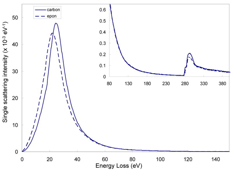
Single scattering spectra for carbon (solid line) and epon embedding material (dashed line) obtained from measured spectra by logarithmic deconvolution. Single scattering distribution is normalized so that its integrated intensity is unity. Inset with expanded intensity scale shows single scattering distribution in the region of the phosphorus L2,3 edge at 132 eV and the carbon K edge at 284 eV. The plasmon peak for epon is shifted 3 eV down in energy loss relative to the plasmon peak for carbon.
Having obtained the single scattering distribution Q(E), we are now able to calculate electron energy loss spectra for relative thicknesses of t/λ from 0.05 to 1.45 by using Eq. 6. These results are shown for carbon in Fig. 2, where it is evident that the background increases nonlinearly as a function of t/λ corresponding to the multiple scattering terms in Eq. 5. We can now easily compute the k0-ratio as a function of t/λ by integrating the spectral intensities over an appropriate energy window of 20 eV above and below the P L2,3 edge at 152 eV and 120 eV, respectively. In Fig. 3 the calculated values of k0 first decrease with increasing thickness until a minimum is reached at a t/λ value of ~0.6 for carbon and ~0.7 for epon, and then the values of k0 increase as higher order plural scattering terms dominate. The slightly narrower shape of the curve for evaporated carbon is due to differences in the single scattering distributions between carbon and epon, which we have described above. To correct for plural scattering in EFTEM imaging, we parameterize the k0-curves by fitting a polynomial through the calculated data points, as shown in Fig. 3, where fifth order polynomials are fitted through the calculated k0-values for both carbon and epon. Since there was a negligible difference between the k0-curve and fitted function, it was unnecessary to use a higher order polynomial. This parameterization enables us to calculate thickness-corrected k0 maps from measured t/λ images. The shape of the k0-curve can be understood by considering three ranges of t/λ. In the range of t/λ ~ 0 to ~0.4, the energy loss spectrum in the vicinity of the P L2,3 edge becomes steeper, which results in a decreasing k0-value. This increased steepness can be explained by double scattering consisting of a plasmon convoluted with the high-energy tail of the valence electron spectrum, which adds a contribution consisting of the same shaped tail but with a shift to a higher energy loss. For specimens of relative thickness greater than one mean free path, multiple scattering pushes the spectral intensity to higher energy losses so that the spectrum actually becomes less steep, which results in an increasing k0-value. Between these two ranges of t/λ where the minimum occurs, the k0-value remains nearly constant. Thus, in this middle thickness range of t/λ ~ 0.5 to ~0.9, the k0-value varies by only ~2%. This surprising result indicates that two-window EFTEM imaging of phosphorus is applicable to specimens that are thicker than previously realized [14]. In fact, this middle range of t/λ is commensurate with typical thicknesses of plastic-embedded biological sections, i.e., 100 nm to 200 nm for an accelerating voltage of 300 kV.
Figure 2.
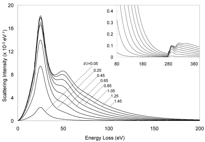
Carbon EELS for t/λ varying from 0.05 to 1.45, calculated from the single scattering distribution. As t/λ increases, the spectral shape changes due to plural scattering. Inset with expanded intensity scale, shows spectra in the region of the phosphorus L2,3 edge and the carbon K edge.
Figure 3.
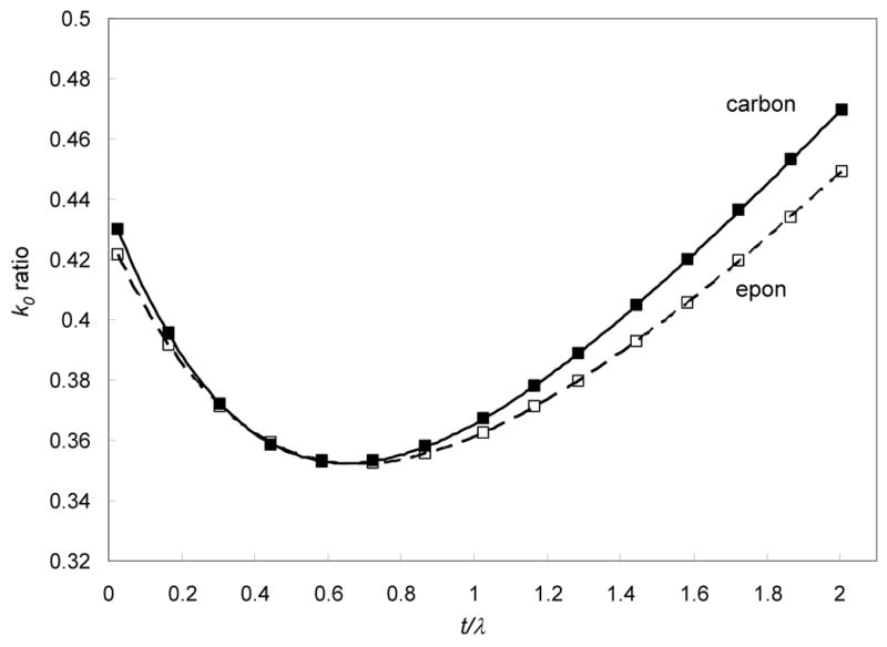
Ratio k0 of EELS intensity in energy band 152±10 eV to intensity in energy band 120±10 eV for carbon (solid squares) and epon embedding material (open squares), obtained from the calculated spectra such as the ones in Fig. 2. These energy bands are the ones used for two-window mapping of phosphorus with the L2,3 edge at 132 eV. Fifth order polynomial fits through the data are also shown for carbon (solid line) and epon (dashed line). For carbon, fitted polynomial was k0 = −0.005(t/λ)5 + 0.049(t/λ)4 − 0.192 (t/λ)3 + 0.397(t/λ)2 − 0.322(t/λ) + 0.438; and for epon k0 = −0.005(t/λ)5 + 0.044(t/λ)4 − 0.162 (t/λ)3 + 0.330(t/λ)2 − 0.275(t/λ) + 0.429.
4. Systematic and statistical errors in two-window elemental maps
Although there exists a thickness range over which the k0-values for the P L2,3 edge remains relatively constant, systematic errors in estimating the background do occur when using the standard two-window EFTEM imaging of phosphorus in specimens of non-uniform thickness. When relatively low concentrations of phosphorus occur in a specimen, it can be important to correct for these effects, which is now facilitated by our knowledge of the k0-curve, together with a measurement of the t/λ map.
The error in the signal estimation obtained by using a value of k0 for one specific thickness, k0′, instead of a thickness-dependent k0 is
| (8) |
where k0 and Ipre are both functions of t/λ. The first term in Eq. 8 is plotted as a heavy line in Figs. 4a and 4b, and the second term is plotted as a series of thinner lines for three values of k0′ corresponding to different specimen thicknesses. The systematic error in the signal estimation obtained by using a constant ratio k0′, rather than a thickness-dependent ratio k0(t/λ), is represented by the difference between the solid line and the thin lines. To help show these differences, the curves are plotted separately for thickness ranges of 0 < t/λ < 1.5 (Fig. 4a) and 0 < t/λ < 0.5 (Fig. 4b).
Figure 4.
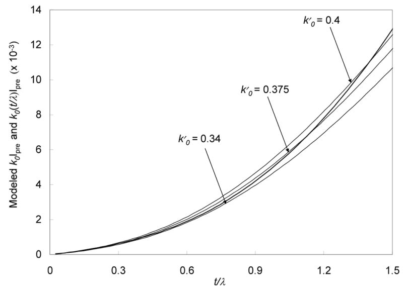
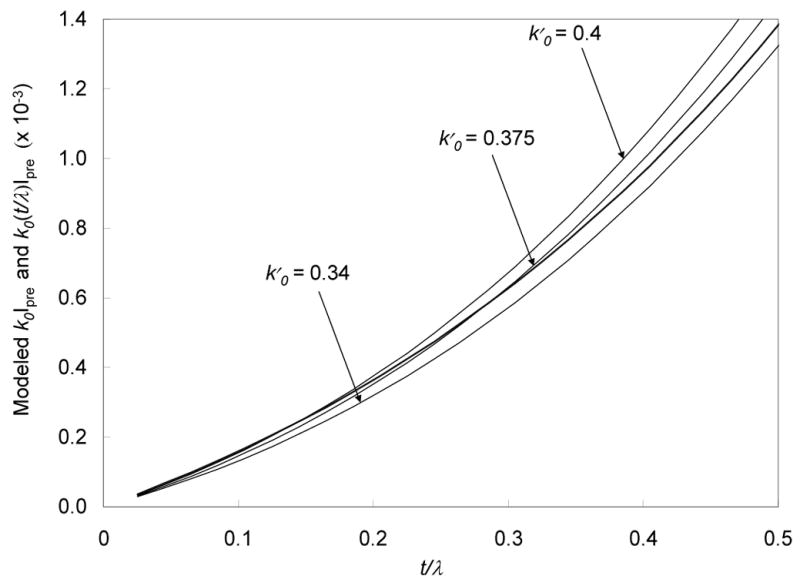
Post-edge background intensity for the phosphorus L2,3 excitation k0(t/λ)Ipre as a function of t/λ, calculated using the curve in Fig. 3 (heavy line), compared with the post-edge background k0’Ipre calculated by assuming constant ratios k0’ for post-edge to pre-edge intensities (thin lines); curves for three different values for k0’ (0.340, 0.375 and 0.400) are indicated. (a) t/λ in the range 0 to 1.5; and (b) t/λ in the range 0 to 0.5. The differences between the heavy line and the thin lines represent the systematic errors in the signal estimation at the phosphorus L2,3 edge.
The number of atoms per unit area n of an element can be determined from the net signal S(Δ,β) in its core edge, measured in an energy band Δ and inside a collection semi-angle β, through the expression [27,28,30,31]:
| (9) |
where σ(Δ,β) is the inelastic scattering cross section for the core level excitation for the energy band Δ and collection semi-angle β and I0(Δ,β) is the measured intensity in the transmitted electron beam, including the zero-loss peak for the same energy band and collection angle. The cross section σ(Δ,β) is obtained from the modified hydrogenic model incorporated into the Gatan EL/P software, as originally described by Egerton [32,33]. Provided that the specimen thickness is smaller than the inelastic mean free path λ and that the energy window Δ is less than about 20 eV, most of the low-loss intensity is contained in the zero-loss peak, in which case I0(Δ,β) can be approximated by the zero-loss intensity I0.
We can also write a similar equation as Eq. 9 for the systematic error in the number of atoms per unit area in terms of the systematic error in the core-edge signal, as given by Eq. 8. The systematic error in n is
| (10) |
Calculated curves for the systematic errors in the number of phosphorus atoms per unit area of a carbon specimen as a function of t/λ are plotted in Fig. 5 for ten values of k0′ from 0.33 to 0.42. Some of these values of k0′ fall outside the range predicted by the k0-curve in Fig. 3 calculated from the measured spectrum. There are two reasons for extending the range of k0′ values. First, the optimal two-window map, without k0-curve correction, is not necessarily obtained by using the k0 value corresponding to the mean specimen thickness. In Fig. 5 we see that the optimal value k0′ for a particular range of t/λ is the one for which the error curve has a minimum in the center of the thickness range, even if there is a substantial offset to the calculated number of phosphorus atoms per unit area. In practice the offset is simply determined by setting the phosphorus intensity to zero in a region of the specimen that is known not to contain the element. Thus, for a specimen having a thickness range of 0.7 < t/λ <1.0, the optimal k0′-value is 0.38; this results in a sizeable systematic error of about −200 phosphorus atoms/nm2, which can be removed subsequently by adding an intensity offset. The second reason for extending the range of k0′ is that experimentally measured k0-values obtained from post-edge and pre-edge images can be slightly different than the ones calculated from the modeled spectra due to the electron optical considerations. When the imaging filter is adjusted to pass electrons of a different energy loss, e.g., from 152 eV to 120 eV, the accelerating voltage of the microscope is changed by the corresponding difference in energy loss. This results in a slightly different focusing action of the condenser lenses in front of the specimen, whereas the action of the post specimen lenses is unaffected because electrons of the same energy pass through the energy-selecting slit. Although the filter controller feeds back digitally into the condenser lens excitation to adjust for changes in focus, this correction is not perfect and there is a change in the spot size as a function of energy loss offset. This effect is greatest when the condenser lens is adjusted close to a crossover at the specimen, which is typically the condition for collecting core-edge image data. Variation in the spot size of 3% results in a change in current and variation in k0-value of 6%, which would change the k0-value by 0.02. We have observed such changes in the FEI Tecnai TF30 and CM120 electron microscopes.
Figure 5.
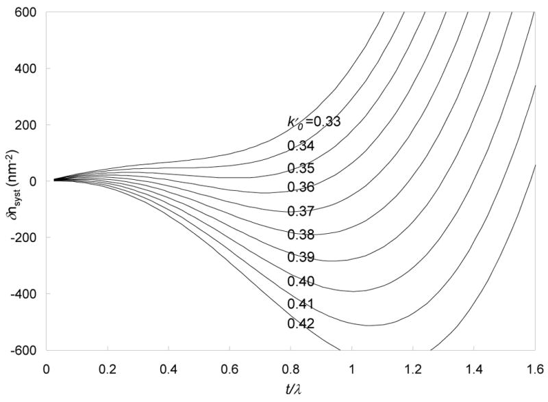
Calculated systematic error δ nsyst in the number of phosphorus atoms per unit area, for ten values of k0’ ranging from 0.33 to 0.42 with increments of 0.01. If there exists a δ nsyst curve that is relatively flat for a given range of t/λ, then a single value of k0 plus an offset can be used for elemental mapping. However, if there is no δ nsyst curve that is flat for that range of t/λ, then it is necessary to use the k0-curve correction.
Next we consider the statistical errors in two-window elemental maps caused by the limited available electron dose on the specimen. We have shown that it is possible to correct for systematic errors in samples as thick as one inelastic mean free path, but we need to take into account the increased statistical error in the extracted core edge signal due to the nonlinear increase in background underlying the core edge. The estimated variance of the signal, var(S), is given by the sum of the variances of the post edge intensity, var(Ipost), and the variance of the pre-edge intensity, var(k0Ipre):
| (11) |
Since k≈k0 for low concentrations of phosphorus, the variance in the signal can be written as,
| (12) |
The statistical error is therefore given by the standard deviation or the square root of the variance:
| (13) |
and the statistical error in the number of atoms per unit specimen area is
| (14) |
The statistical error in the number of phosphorus atoms per unit area is plotted logarithmically as a function of t/λ for different numbers of incident electrons in Fig. 6, from which it is evident that the statistical error increases by an order of magnitude when the specimen thickness increases from 0.5 to 1.5 mean free paths. For thin specimens with a t/λ of 0.2 and 107 electrons per pixel, Eq. 14 predicts that it should be feasible to detect 10 phosphorus atoms/nm2.
Figure 6.
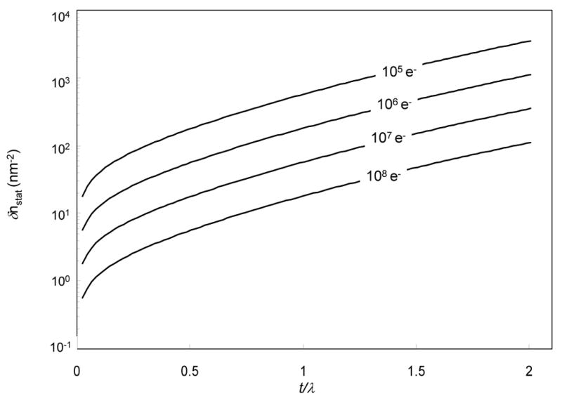
Calculated statistical error in number of phosphorus atoms per unit area as a function of t/λ plotted on a logarithmic scale; values correspond to one standard deviation a measurement of phosphorus in a carbon matrix. Statistical errors are shown for four different incident numbers of electrons (105, 106, 107 and 108) and for an accelerating voltage of 300 kV.
Typically, elemental maps are acquired from specimens with a thickness of 0.5 mean free paths and with exposures of 105 electrons per pixel, which would give a predicted statistical error of about 200 atoms/nm2. The form of Eq. 14 is simpler than previous analyses based on three-window mapping [28,34,35].
5. Results and Discussion
We first test our correction scheme on overlapping layers of an evaporated carbon film, in which no phosphorus is present. Unfiltered and zero-loss images recorded with an incident beam energy of 300 keV from a specimen region containing 4, 5 and 6 layers of carbon, each with a thickness of approximately 0.2 inelastic mean free paths, are shown in Figs. 7a and 7b respectively, from which it is straightforward to compute the t/λ map, as shown in Fig. 7c. A horizontal line profile, averaged over 50 pixels in the vertical direction to reduce statistical noise, is included under each image. Energy-selected images recorded at energy losses of 152 ± 10 eV and 120 ± 10 eV, corresponding to the post-edge and pre-edge windows for the phosphorus L2,3 excitation, are shown in Figs. 7d and 7e, respectively, and their ratio is displayed in Fig. 7f. Horizontal line profiles are again included below each image, from which it is seen that the k0-value varies from ~0.33 to ~0.36. In Figs. 7g, 7h and 7i we compare three different methods for determining the net phosphorus signal. The image in Fig. 7g was calculated using a single value for k0′ = 0.33 corresponding to the observed value in the thinnest region of the specimen. It is evident that the thickness effects are not corrected under these conditions. The fact that the observed k0-value is lower than expected from the k0-curve in Fig. 3 is explained by variations in condenser illumination when the energy loss offset is changed, as discussed above. The image in Fig. 7h was calculated by applying an adjusted k0-value of 0.375 and an offset of 100 counts. Using these parameters, we are able to correct for thickness variation across the boundary between 4 and 5 layers of carbon, but we are unable to correct for thickness changes across the boundary between 5 and 6 layers of carbon. This result can be understood from Fig. 5, where there are no flat regions in any of the error curves for different k0′ when t/λ varies from 0.8 to 1.2. To correct for plural scattering effects across the full range of thicknesses, it is necessary to apply the thickness-dependent k0-ratio method, the result of which is shown in Fig. 7i. As seen by the horizontal line profile across Fig.7i, the signal intensity S fluctuates around a constant value across the whole field, as expected for a specimen that contains no phosphorus. The constant level was set to zero by applying an offset, as described above.
Figure 7.
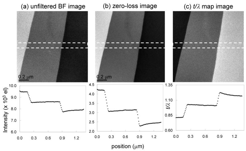
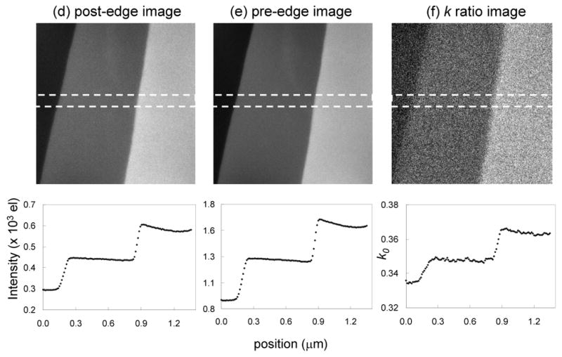
(a) Unfiltered image and (b) zero-loss image acquired from evaporated carbon film with overlapping layers; and (c) calculated t/λ map showing thickness variation from 0.8 to 1.2 inelastic mean free paths; horizontal line profiles are displayed below each panel; accelerating voltage was 300 kV. (d) Post-P L2,3 edge image, (e) pre-P L2,3 edge image, and (f) k-ratio image; line profiles are indicated. (g) Calculated P L2,3 signal with k0’ value of 0.335 reveals spurious intensities across the three layers. (h) Calculated signal with an adjusted k0’ value of 0.375 shows elimination of intensity difference across the two layers on the left side of the image but not between the two layers on the right. (i) Calculated signal obtained using the full k0-curve correction, showing elimination of contrast differences across all three layers; the narrow residual features at the boundaries of the layers are attributed to slight misalignment between the core-edge images and the low-loss images. The magnitude of intensity differences across the layers in images (g)–(i) can be seen in the line profiles below each panel.
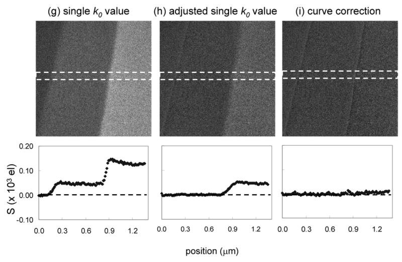
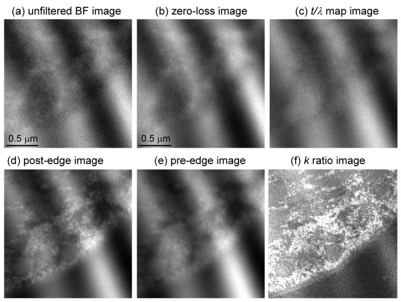
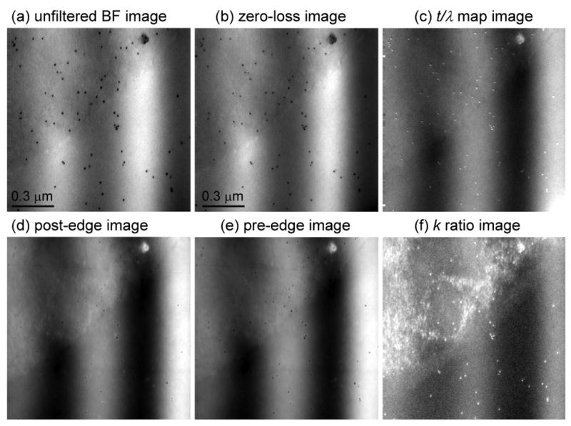
Next we apply the thickness-dependent k0-ratio correction scheme to map the distribution of phosphorus in a sectioned epon-embedded cell from a Drosophila larva. Figs. 8a, 8b and 8c show unfiltered, zero-loss and t/λ images, respectively, recorded at an incident beam energy of 300 keV from a sectioned cell that has a thickness ranging from 0.25 to 0.45 inelastic mean free paths. The diagonal bands in the t/λ image are due to compression during ultramicrotomy. These thickness variations are also observed in the phosphorus L2,3 post-edge and pre-edge images in Figs. 8d and 8e, and it is evident that they are not completely canceled in the ratio map displayed in Fig. 8f. The same thickness related artifacts are observed again in the distribution of phosphorus atoms per unit area calculated by using a single k0′-value of 0.34, as shown in Fig. 8g. By selecting a smaller k0′-value of 0.33 and adding an appropriate offset, we can eliminate the thickness artifacts in the phosphorus distribution, as shown in Fig. 8h. A full correction using a t/λ dependent k0-curve, shown in Fig. 8i, gives the same result as for Fig. 8h, demonstrating that it is not necessary to use the full correction scheme in a specimen for which t/λ values vary from 0.2 to 0.5. The accuracy and precision of the analyses can be assessed by the horizontal line profiles, each of which reveals a variation of ± 10 phosphorus atoms per nm2. The bright features in the phosphorus distributions are identified as ribosomes, which are distributed throughout the cytoplasm. As expected, the phosphorus per unit area is higher in the compressed regions of the specimen with greater t/λ values, whereas in the areas of the specimen containing only embedding material, the phosphorus distribution remains close to zero across the both the thicker and thinner regions.
Figure 8.
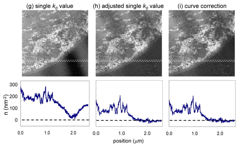
(a) Unfiltered image and (b) zero-loss image from part of an epon-embedded cell of Drosophila larva; and (c) calculated t/λ map showing thickness variation from 0.25 to 0.45 inelastic mean free paths, due to compression in preparation of sections; accelerating voltage was 300 kV. (d) Post-P L2,3 edge image, (e) pre-P L2,3 edge image, and (f) k-ratio image. (g) Calculated distribution of phosphorus per unit area assuming a single k0’ value of 0.343 reveals spurious intensity variations that follow the thickness variations in the epon; (h) Calculated distribution of phosphorus using an adjusted k0’ value of 0.33 eliminates intensity variations in the epon; (i) Calculated distribution of phosphorus using the full k0-curve correction gives the same result as in (h); horizontal line profiles shown below images (g)–(i) were averaged in vertical direction over 10 pixels.
Finally, we test our thickness correction scheme on a specimen that has a larger value of t/λ. Figs. 9a, 9b and 9c show unfiltered, zero-loss and t/λ images, respectively, from a sectioned cell of Drosophila larva. The corresponding post-edge, pre-edge and k-ratio images are shown in Figs. 9d, 9e and 9f, respectively. The images were recorded at a beam energy of 120 keV from a specimen that was tilted to an angle of 60° in order to double the value of t/λ in the beam direction. The need to record reliable elemental maps from tilted specimens arises in energy filtered electron tomography, in which the distributions of specific elements are reconstructed in three dimensions from tilt series [17]. In fact, the specimen used to obtain the images in Fig. 9 was prepared for EFTEM tomography and its surfaces were coated with 10-nm gold particles to facilitate alignment of the images from the tilt series, which are visible in all the panels of Fig. 9. The t/λ values in Fig. 9c range from 0.7 to 1.2 due to compression during sectioning. These thickness variations are large enough to introduce significant changes in spectral shape across the specimen; they are also seen clearly in Fig. 9f, where the bands of compression run across the cell into the plastic embedding material. The same thickness related artifacts are observed again in the distribution of phosphorus atoms calculated by using a single k0′-value of 0.345, as shown in Fig. 9g. By selecting an optimized single k0′ value of 0.385, we are able to reduce but not eliminate the thickness-dependent artifacts in the phosphorus map, which can be explained by the nonlinearity of the k0Ipre in the thickness range of this specimen. As shown in Fig. 9i, a full correction using the t/λ dependent k0-curve takes account of this nonlinearity and almost eliminates the thickness-dependent artifacts in the calculated phosphorus distribution. The effect of the three different background subtraction schemes can be assessed by the horizontal line profiles through the center of the image and averaged over 10 pixels in the vertical direction. In Fig. 9i, the calculated phosphorus distribution with the k0-curve correction fluctuates close to zero in the extracellular region of epon on the right side of the image, whereas large oscillations in apparent phosphorus concentrations are present in the maps obtained using constant k0-values.
Figure 9.
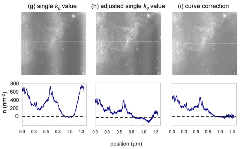
(a) Unfiltered image and (b) zero-loss image from part of an epon-embedded cell of Drosophila larva; and (c) calculated t/λ map showing thickness variation from 0.7 to 1.2 inelastic mean free paths, due to compression during preparation of sections; sample was tilted to angle of 60° to increase t/λ values deliberately and accelerating voltage was 120 kV; 10-nm gold particles deposited on the surface of this specimen are visible as dark features in the bright-field low-loss images and bright features in the inelastic images. (d) Post-P L2,3 edge image, (e) pre-P L2,3 edge image, and (f) k-ratio image. (g) Calculated distribution of phosphorus per unit area assuming a single k0’ value of 0.345 reveals spurious intensity variations that follow the thickness variations in the epon. (h) Calculated distribution of phosphorus using an adjusted k0’ value of 0.385 reduces but does not eliminate intensity variations in the epon. (i) Calculated distribution of phosphorus using the full k0-curve correction eliminates the intensity variations in the epon. Horizontal line profiles shown below images (g)–(i) were averaged in vertical direction over 10 pixels.
We anticipate that our thickness correction scheme could be used to map other elements such as sulfur, calcium or iron in biological specimens. However, application of the method will be complicated if there are overlapping features in the energy loss spectrum. For example, in the case of calcium, the strong carbon K edge at 285 eV is quite close in energy loss to the Ca L2,3 edge at 348 eV. Double scattering involving a plasmon plus a C K excitation can therefore drastically change the shape of the background underlying the Ca L2,3 edge [36–38]. The thickness correction in two-window mapping of calcium will therefore be much more difficult to apply than for phosphorus mapping. In such cases, there is an advantage in using an EFTEM spectrum-imaging technique, in which a series of energy-selected images are acquired in the vicinity of a core edge [22,23,39]. In this way, it is possible to build up an energy-loss spectrum at each pixel in an image, which allows more flexibility in background subtraction. The disadvantage of EFTEM spectrum-imaging is that the acquisition time and electron dose are increased.
6. Conclusions
We have shown that it is possible to correct for thickness variations in EFTEM elemental mapping by modeling small changes in the ratio of post-edge to pre-edge intensities as a function of specimen thickness measured in terms of the inelastic mean free path. The method has the advantage of retaining the two-window approach and only requires the additional acquisition of an unfiltered low-loss image and a zero-loss image, which provides a thickness map of the specimen and hence the distribution of post-edge to pre-edge intensity ratios. We have demonstrated the technique by mapping phosphorus in specimens that have large variations in thickness. The results show that reliable quantitative distributions of phosphorus can be obtained from specimens that are as thick as 1.2 inelastic mean free paths. The technique could be applied to map other elements including sulfur and calcium in biological systems, as well as certain types of non-biological materials such as polymers or amorphous solids. We anticipate that the correction scheme will be particularly useful for performing elemental tomography, which requires that specimens be tilted to about 70°, with a concomitant increase in specimen thickness by a factor of three. Our analysis also provides a framework for a detailed understanding of the systematic and statistical errors in EFTEM mapping of biological specimens and should be useful for assessing detection limits for phosphorus imaging of nucleic acid in unstained plastic sections. Furthermore, the results explain why uncorrected two-window EFTEM mapping of phosphorus can be applied successfully to thicker specimens than would be expected if it were simply assumed that errors increased monotonically with specimen thickness.
Acknowledgments
This research was supported by the Intramural Research Program of the National Institutes of Health.
Footnotes
Publisher's Disclaimer: This is a PDF file of an unedited manuscript that has been accepted for publication. As a service to our customers we are providing this early version of the manuscript. The manuscript will undergo copyediting, typesetting, and review of the resulting proof before it is published in its final citable form. Please note that during the production process errorsmaybe discovered which could affect the content, and all legal disclaimers that apply to the journal pertain.
References
- 1.Reimer L. Energy-Filtering Transmission Electron Microscopy. Berlin: Springer; 1995. [Google Scholar]
- 2.Egerton RF. Micron. 2003;34:127. doi: 10.1016/s0968-4328(03)00023-4. [DOI] [PubMed] [Google Scholar]
- 3.Gubbens AJ, Brink HA, Kundmann MK, Friedman SL, Krivanek OL. Micron. 1998;29:81. [Google Scholar]
- 4.Krivanek OL, Friedman SL, Gubbens AJ, Kraus B. Ultramicroscopy. 1995;59:267. doi: 10.1016/0304-3991(95)00034-x. [DOI] [PubMed] [Google Scholar]
- 5.Brink HA, Barfels MMG, Burgner RP, Edwards BN. Ultramicroscopy. 2003;96:367. doi: 10.1016/S0304-3991(03)00102-5. [DOI] [PubMed] [Google Scholar]
- 6.Benner G, Essers E, Huber B, Lang G, Matijevic M, Orchowski A, Rau WD, Schindler B, Schlossmacher P, Thesen A. Microsc Microanal. 2004;10(Suppl 2):860. [Google Scholar]
- 7.Hunt JA, Kothleitner G, Harmon R. Microsc Microanal. 1999;5(Suppl 2):616. [Google Scholar]
- 8.Hofer F, Warbichler P. In: Transmission Electron Energy Loss Spectrometry in Materials Science and the EELS Atlas. 2. Ahn C, editor. Wiley-VCH; Berlin: 2004. p. 159. Chapter 6. [Google Scholar]
- 9.Ottensmeyer FP. J Ultrastruct Res. 1984;88:121. doi: 10.1016/s0022-5320(84)80004-0. [DOI] [PubMed] [Google Scholar]
- 10.Bazett-Jones DP, Leblanc B, Herfort M. T Moss Science. 1994;264:1134. doi: 10.1126/science.8178172. [DOI] [PubMed] [Google Scholar]
- 11.Bazett-Jones DP, Hendzel MJ, Krulak MJ. Micron. 1999;30:157. doi: 10.1016/s0968-4328(99)00019-0. [DOI] [PubMed] [Google Scholar]
- 12.Wang YY, Ho R, Shao Z, Somlyo AP. Ultramicroscopy. 1992;41:11. doi: 10.1016/0304-3991(92)90091-w. [DOI] [PubMed] [Google Scholar]
- 13.Leapman RD, Rizzo NW. Ultramicroscopy. 1999;78:251. doi: 10.1016/s0304-3991(99)00031-5. [DOI] [PubMed] [Google Scholar]
- 14.Leapman RD. Ann NY Acad Sci. 1986;483:326. doi: 10.1111/j.1749-6632.1986.tb34539.x. [DOI] [PubMed] [Google Scholar]
- 15.Leapman RD, Ornberg RL. Ultramicroscopy. 1988;24:251. doi: 10.1016/0304-3991(88)90314-2. [DOI] [PubMed] [Google Scholar]
- 16.Midgley PA, Weyland M. Ultramicroscopy. 2003;96:413. doi: 10.1016/S0304-3991(03)00105-0. [DOI] [PubMed] [Google Scholar]
- 17.Leapman RD, Kocsis E, Zhang G, Talbot TL, Laquerriere P. Ultramicroscopy. 2004;100:115. doi: 10.1016/j.ultramic.2004.03.002. [DOI] [PubMed] [Google Scholar]
- 18.Frank J. Electron Tomography: Three-dimensional Imaging with the Transmission Electron Microscope. Plenum press; New York: 1992. [Google Scholar]
- 19.Koster AJ, Grimm R, Typke D, Hegerl R, Stoschek A, Walz J, Baumeister W. J Struct Biol. 1997;120:276. doi: 10.1006/jsbi.1997.3933. [DOI] [PubMed] [Google Scholar]
- 20.Marsh BJ, Mastronarde DN, Buttle KF, Howell KE. JR McIntosh Proc Natl Acad Sci USA. 2001;98:2399. doi: 10.1073/pnas.051631998. [DOI] [PMC free article] [PubMed] [Google Scholar]
- 21.Leapman RD, Jarnik M, Steven AC. J Struct Biol. 1997;120:168. doi: 10.1006/jsbi.1997.3937. [DOI] [PubMed] [Google Scholar]
- 22.Goping G, Pollard HB, Srivastava M, Leapman R. Microsc Res Tech. 2003;61:448. doi: 10.1002/jemt.10294. [DOI] [PubMed] [Google Scholar]
- 23.Thomas PJ, Midgley PA. Ultramicroscopy. 2001;88:179. doi: 10.1016/s0304-3991(01)00077-8. [DOI] [PubMed] [Google Scholar]
- 24.Leapman RD, Fiori CE, Swyt CR. J Microscopy. 1984;133:239. doi: 10.1111/j.1365-2818.1984.tb00489.x. [DOI] [PubMed] [Google Scholar]
- 25.Müller-Reichert T, Hohenberg H, O’Toole ET, McDonald K. J Microsc. 2003;212:71. doi: 10.1046/j.1365-2818.2003.01250.x. [DOI] [PubMed] [Google Scholar]
- 26.Batson PE, Silcox J. Phys Rev B. 1983;27:5224. [Google Scholar]
- 27.Egerton RF. Electron Energy Loss Spectroscopy. 2. Plenum Press; New York: 1996. [Google Scholar]
- 28.Leapman RD. In: Transmission Electron Energy Loss Spectrometry in Materials Science and the EELS Atlas. 2. Ahn C, editor. Wiley-VCH; Berlin: 2004. p. 49. Chapter 3. [Google Scholar]
- 29.Leapman RD, Swyt CR. Ultramicroscopy. 1988;26:393. doi: 10.1016/0304-3991(88)90239-2. [DOI] [PubMed] [Google Scholar]
- 30.Egerton RF. Ultramicroscopy. 1978;3:243. doi: 10.1016/s0304-3991(78)80031-x. [DOI] [PubMed] [Google Scholar]
- 31.Isaacson M, Johnson D. UItramicroscopy. 1975;1:33. doi: 10.1016/s0304-3991(75)80006-4. [DOI] [PubMed] [Google Scholar]
- 32.Egerton RF. Ultramicroscopy. 1979;4:169. [Google Scholar]
- 33.Egerton RF. In: Proc. 39th Ann. Meeting of Electron Microsc. Soc. Am. Bailey GW, editor. Claitor's Publishing; Baton Rouge, Louisiana: 1981. p. 198. [Google Scholar]
- 34.Egerton RF. Ultramicroscopy. 1982;9:387. [Google Scholar]
- 35.Unser M, Ellis JR, Pun T, Eden M. J Microsc. 1987;145:245. [PubMed] [Google Scholar]
- 36.Shuman H, Somlyo AP. Ultramicroscopy. 1987;21:23. doi: 10.1016/0304-3991(87)90004-0. [DOI] [PubMed] [Google Scholar]
- 37.Leapman RD, Hunt JA, Buchanan RA, Andrews SB. Ultramicroscopy. 1993;49:225. doi: 10.1016/0304-3991(93)90229-q. [DOI] [PubMed] [Google Scholar]
- 38.Feng J, Somlyo AV, Somlyo AP. J Microsc. 2004;215:92. doi: 10.1111/j.0022-2720.2004.01342.x. [DOI] [PubMed] [Google Scholar]
- 39.Hunt JA, Williams DB. Ultramicroscopy. 1991;38:47. [Google Scholar]