Abstract
Scanning probe microscopy has become a powerful tool to detect structural changes in small clusters of atoms. Herein, we use an atomic force microscope to measure the length of gold nanowire structures during extension and compression cycles. We have found that nanowires elongate under force in quantized steps of up to three integer multiples of 1.76 Å and that they shorten spontaneously in steps of 1.52 Å. Our results can be explained by the sliding of crystal planes within the gold nanowires creating stacking faults that change the local structure from face-centered cubic to hexagonal close packed. Our data also show that there can be up to three simultaneous slip events, in good agreement with the tetrahedral arrangement of slip planes in a gold crystal. These experiments provide direct evidence for the mechanism underlying the plastic deformation of a nanowire. A similar approach can be used to examine the atomic events underlying the plastic failure of other metals and their alloys.
Nanowires are easily formed between metal contacts that are pushed together and have been investigated because of their promise as conductors in mesoscopic scale electronic devices (1–18). Nanowires exhibit quantized ballistic electronic conductance (10–17) and a yield strength that can be more that 20 times bigger than bulk (1, 3, 5–9). Gold nanowires, when placed under a stretching force, undergo atomic rearrangements (1–9) until they form single atom wires and then break (1, 14, 16, 17, 19). On elongation, nanowires are thought to reach configurations that are similar to those observed in atomic clusters including the assembly of “magic number” cluster structures (15, 17). Herein, we use an atomic force microscope (AFM; ref. 20) in air and at room temperature to form gold nanowires and to monitor their length during elongation/compression cycles. We find that nanowires elongate and shorten in quantized steps whose lengths correspond to the forced displacements of the {111} crystal planes that produce stacking faults in the gold lattice (21).
Materials and Methods
AFM.
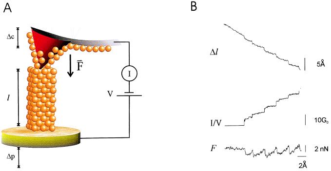
Our custom-made AFM apparatus as well as its mode of operation are identical to apparatuses that we have described recently (22, 23). The AFM was constructed with a Digital Instruments (Santa Barbara, CA) AFM detector head mounted on top of a single-axis piezoelectric actuator. Data acquisition and control of the piezo movement were done simultaneously with a personal computer mounted data acquisition board (AT-MIO-16X; National Instruments, Austin, TX) with custom-written software (labview, National Instruments). The AFM cantilevers (TappingMode Etched Silicon Probe, Digital Instruments) had a spring constant, kc, of 20–100 N/m. The length of the nanowires was calculated by subtracting the cantilever deflection from the travel of the piezoelectric actuator (Δl = Δp − Δc; see Fig. 1).
Figure 1.
(A) Schematic of the experimental set-up used to measure the length and conductance of single gold nanowires. The figure depicts an AFM cantilever, coated with gold, making contact with a nanowire. A piezoelectric positioner moves the nanowire by Δp, which results in a deflection of the cantilever by Δc. During compression or extension cycles, the change in length of the nanowire is measured as Δl = Δp − Δc. The cantilever exerts a force F = kΔc on the nanowire, where k is the cantilever spring constant. Together with the changes in length, Δl, we also measure the nanowire conductance G. (B) An example of simultaneous recordings of Δl, G = I/V, and F obtained on compressing a gold nanowire.
Gold Nanowires.
Glass coverslips were coated with 40 nm of chromium/nickel (80Cr/20Ni; Goodfellow, Cambridge, England) and 100 nm of pure gold (99.99%; Goodfellow) with a high vacuum evaporator (Edwards, Wilmington, MA). AFM cantilevers were coated on both sides with a 20-nm layer of chromium/nickel and a 50-nm layer of gold. Gold nanowires were formed in air and at room temperature by pressing a gold-coated AFM cantilever against a gold-coated coverslip. The electrical conductance of gold nanowires was measured by clamping the voltage across the AFM tip and the gold-coated coverslip and measuring the resulting current by means of a current-to-voltage converter with a 50-kΩ feedback resistor.
Results and Discussion
Gold nanowires, a few atoms across and 5–10 nm long, were readily formed in air and at room temperature by pressing a gold-coated AFM cantilever (spring constants = 20–100 N/m) against a gold-coated coverslip. Fig. 1A shows a schematic diagram of our set-up. The nanowires could be compressed by a few nanometers and then stretched back by moving a piezoelectric actuator that pushed or pulled the nanowire against the AFM cantilever (1–9). During these cycles, we measured the force (F; Fig. 1 A and B) applied to the nanowire and monitored its length (l) by subtracting the displacement of the piezoelectric actuator from the movement of the cantilever, Δl = Δp − Δc (Fig. 1 A and B). In addition to measuring force and length, we also simultaneously measured the nanowire conductance (G; Fig. 1 A and B), which is an estimate of the cross-sectional area of the nanowire contact, valid in the Sharvin limit (8, 9). Fig. 1B shows a typical recording of Δl, G, and F obtained on compressing a gold nanowire. As shown before, the compressive force on a nanowire varies in a sawtooth pattern with peaks of ≈2 nN, which coincide with step increases in nanowire conductance (7). We have found that during these cycles, the length of the nanowire also changes in a stepwise manner (Δl, Fig. 1B) and that measurements of length can describe the plastic deformation of a nanowire accurately.
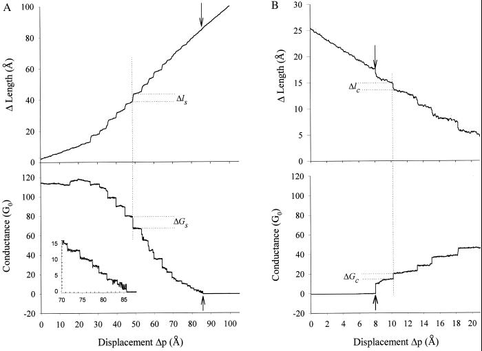
In Fig. 2, we show details of simultaneous recordings of length and conductance measured on pulling and compressing gold nanowires with our AFM instrument. The tensile phase of the cycle shows both elastic and plastic deformations (Fig. 2A). The elastic deformation is observed easily at the beginning of the recording and is characterized by a continuous increase in the length of the nanowire, while, at the same time, the conductance declines slightly. During the forced extension, a point is reached where the accumulated strain is relieved by a plastic event that results in a stepwise elongation of the nanowire, simultaneously causing a step reduction in conductance (1). The nanowire continues to elongate with a mixture of clearly distinguishable elastic and plastic events until the contact between the tip and the nanowire breaks (Fig. 2A, arrow). During the compressive phase, the nanowires also shorten with a mixture of elastic and plastic events (Fig. 2B, arrow). Initially, the AFM tip jumps to contact with the nanowire, which then begins to shorten in steps (Fig. 2B). These plastic events are accompanied by step increases in conductance. In the early phase of nanowire shortening, we observed that many steps occurred spontaneously at a negligible applied force (<100 pN; not shown). Thus, on reestablishing contact with the AFM tip, the nanowires undergo spontaneous shortening.
Figure 2.
Stepwise changes in length and conductance of gold nanowires during a stretching and compression cycle. (A) During stretching, a nanowire elongates in steps (Δls; Upper). Each step increase in length typically coincides with a step reduction in conductance (ΔGs; Lower). The arrows indicate the point at which the nanowire breaks. (Inset) Amplified record of the conductance steps just before breaking off. (B) During compression, a nanowire also shortens in steps (Δlc; Upper), each of which coincides with step increases in conductance (ΔGc; Lower). The arrows indicate the point at which the AFM tip contacts the nanowire for the first time. The nanowire conductance is shown in units of G0, the quantum unit of ballistic electronic conductance (G0 ≈ 77 μS). The abscissa in all records corresponds to Δp, calibrated in Å.
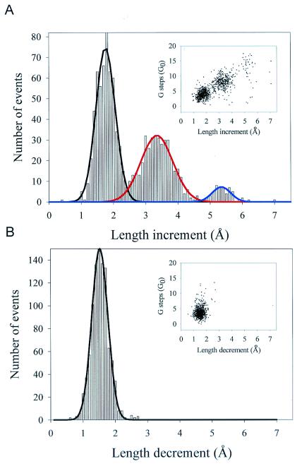
Fig. 3A shows a histogram of the size of the elongation steps. The figure shows three distinct peaks at 1.76 Å, 3.35 Å, and 5.35 Å, showing that elongation occurs in integer multiples of ≈1.7 Å. The magnitude of the elongation step is correlated only loosely with the magnitude of the corresponding step decrease in conductance, with several step elongation events showing no change in conductance (Fig. 3A Inset). Fig. 3B shows a histogram of the shortening step sizes. In this case, we observe a distribution with a single peak at 1.52 Å. Step shortenings also correlate poorly with the size of the corresponding step increases in conductance (Fig. 3B Inset).
Figure 3.
Histograms of the quantized changes in length observed during the extension or compression of gold nanowires. (A) Histogram of Δls values (n = 1,000). Gaussian fits to the individual peaks of the histogram give distributions that peak at 1.76 Å, 3.35 Å, and 5.35 Å (solid lines). (Inset) The relationship between the conductance steps, ΔGs, and the length increments, Δls. (B) Histogram of Δlc values (n = 776). A Gaussian fit to the data peaks at 1.52 Å (solid line). (Inset) The relationship between the conductance steps, ΔGc, and the length decrements, Δlc.
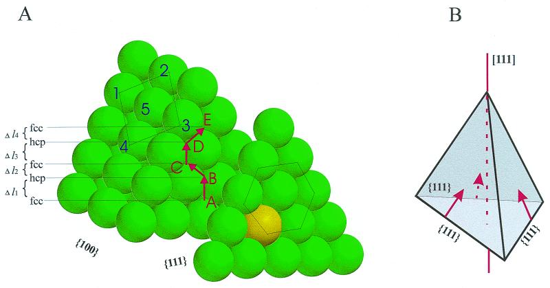
It is generally accepted that plastic elongation of a gold face-centered cubic (fcc) crystal structure involves the sliding of {111} planes with respect to each other (4, 19, 21). Recent experiments demonstrated that gold nanowires could be pulled into single atom wires characterized by a ballistic electronic conductance of ≈77 μS (G0; refs. 14 and 16). In these experiments, the single-atom wires were observed to break at lengths that were multiple integers of 3.6 Å (or 2.7 Å, see footnote 21 in ref. 24), lengths that were related to the stretched Au–Au bond length (14). In contrast to these results, the forced elongation of the thicker nanowires reported herein occurs in steps of ≈1.7 Å, a length that does not match that of the Au–Au bond (2.88 Å) or the interlayer distance of an fcc gold crystal (2.04 Å). The discrepancy becomes even larger if we take into account that the gold nanowires are typically stretched by ≈15 nN of force. Hence, it is likely that the magnitude of the quantized elongation events results from the geometry of the sliding of crystal planes in the nanowires. Fig. 4A examines this possibility. Although gold atoms form an fcc lattice, the sliding of a {111} plane will alternatively form either an fcc or a hexagonal-close packed (hcp) structure with its neighbors (21). These events (fcc-to-hcp transitions) form structures known as stacking faults and are thought to be of common occurrence during plastic deformation (4, 19, 21). Fig. 4A shows a gold crystal oriented in the [111] direction and traces the path of a gold atom during consecutive slide events of a {111} plane, which is inclined to the [111] direction at 19.5°. The {111} planes begin as fcc and then, after a first step (Fig. 4A,  ,
,  | = 1.66 Å), become hcp, and a subsequent step packs the planes again into an fcc lattice (Fig. 4A,
  , |
, | | = 1.66 Å). The first fcc-to-hcp transition contributes with a total displacement of Δl = 1.66 Å⋅cos(19.5°) = 1.56 Å in the z axis, which is close but not exactly the value observed experimentally. By contrast, the second transition (hcp to fcc) occurs at an angle of 60° and is calculated to contribute with a much smaller step size of only Δl = 0.78 Å, which we do not observe. Table 1 shows the calculated values of Δl predicted for fcc-to-hcp transitions for various crystal orientations. It is unlikely that the nanowires have a single, well defined crystalline structure. We speculate that there will be a mixture of crystalline domains oriented randomly, intermixed with dislocations and stacking faults.
Figure 4.
A model for the quantized plastic elongation of a gold nanowire. (A) A nanowire has been cleaved along {111} planes to expose the slippage of a neighboring layer during plastic deformation. The atoms labeled 1–5 show the standard fcc arrangement of gold. The red line marks the stepwise trajectory of an atom from the slipping plane (gold colored). The slip results in the formation of a stacking fault and creation of a locally hcp crystal structure (AB transition). A subsequent slip (BC transition) restores the local structure back to the fcc arrangement. The slips displace the {111} planes by 1.66 Å each time. However, their contribution to the elongation of the nanowire will depend on their relative inclination with respect to the pulling direction (e.g., Δl1, Δl2, etc.; see Table 1). (B) Tetrahedral arrangement of {111} planes when the crystal is oriented in the [111] direction. Stacking faults can occur in one or all of the {111} planes that are oriented toward the pulling direction (three planes in this case; see Table 1).
Table 1.
Predicted length increments of a gold nanowire caused by the fcc–hcp slips in the {111} plane at different crystal orientations of the wire axis
| Crystal orientation | Direction
|
||
|---|---|---|---|
| [111] | [110] | [100] | |
| {111} Inclination* | 19.5° | 54.7° | 35.3° |
| Δlfcc–hcp | 1.56 Å (94%)† | 0.96 Å (58%)† | 1.36 Å (82%)† |
| Δlhcp–fcc | 0.78 Å (47%)† | 0.48 Å (29%)† | 0.88 Å (53%)† |
| No. of {111} planes | 3 | 2 | 4 |
The inclination angle of the {111} planes relative to the pulling direction. We assume that, in each case, the direction of the applied force coincides with the wire axis (crystal orientation).
Percentage of the force acting in the slip direction.
Schmid's law (21) predicts that the preferred slippage modes will be those that experience the greatest component of the force in the slip direction. Therefore, in the case of the nanowires, the preferred slippage will be {111} planes undergoing fcc-to-hcp transitions in a crystal oriented in the [111] direction (Table 1). It is also suggestive that the histogram of Fig. 3A shows three distinct peaks, in agreement with the fact that, in the [111] orientation, there are three {111} planes that can slide with high probability (Table 1). The maximal predicted step elongation (Δl = 1.56 Å) is smaller than the observed first peak of the distribution (Fig. 3A; Δl1 = 1.76 Å). However, the calculations of Table 1 were done for a relaxed gold crystal, whereas our measurements are done under an applied force. Nanowire stretching was done typically under an average pulling force of 15 nN (n = 1,000, where n is the number of measured steps). The elongation events of the first peak in the distribution shown in Fig. 3A occurred at an average force of 12.2 nN (n = 557) and an average conductance of G = 52 G0 (n = 557), which corresponds to a cross-sectional area of 4.16 nm2 (calculated as Ac ≈ 0.08⋅G/G0 nm2; ref. 8). Assuming a Young's modulus of ≈40 × 109 N/m2 (7), we calculate a stretched Δl = 1.67 Å, which is close to our experimental observations.
As shown in Fig. 2, after stretching a nanowire to the point of rupture, we reversed the direction of the piezoelectric actuator and brought the AFM tip back in contact with the standing nanowire structure. As soon as contact was reestablished, the nanowire tended to collapse on its own, pulling the cantilever down with each shortening step and generating a pulling force of F = 1.35 nN (n = 776). Only after this force was relaxed to zero by steadily moving the nanowire up against the cantilever could a new shortening step be observed. A histogram of the steps obtained this way is shown in Fig. 3B. This time, the distribution of step sizes is represented by a single peak with a step size of Δl = 1.52 Å. Higher multiples are not observed, probably because the pulling force developed by a spontaneous shortening step will prevent their occurrence. Because these spontaneous shortening steps were obtained at F = 1.35 nN (n = 776) and an average conductance G = 23.2 G0 (n = 776), we calculate that the bonds are stretched by less than 1%. Hence, the distribution of step sizes shown in Fig. 3B (Δl = 1.52 Å) is a better measure of the slippage distance and is in excellent agreement with the predicted {111} slippage of gold crystals oriented in the [111] direction (Δl = 1.56 Å; see Table 1).
Our experimental results show that nanowire elongation events are quantized following Δl = n⋅1.76 Å, where n = 1, 2, or 3. These observations suggest elongation steps that involve one, two, or three simultaneous {111} slip events. Molecular dynamics simulations of nanowire stretching have predicted that the plastic extension of gold nanowires is due to the slippage of {111} planes (4, 19). Furthermore, these simulations predicted that a principal mode of sliding was due to a “three-plane slip” mechanism where stacking faults would occur in all three faces of the slip tetrahedron (ref. 19; also see Fig. 4B). Our observations strongly suggest that three-plane slips do occur but at a probability lower than that of either two- or just one-plane slips (see Fig. 3A).
Abbreviations
- AFM
atomic force microscope/microscopy
- fcc
face-centered cubic
- hcp
hexagonal close packed
Footnotes
This paper was submitted directly (Track II) to the PNAS office.
References
- 1.Landman U, Luedtke W D, Burnham N A, Colton R J. Science. 1990;248:454–461. doi: 10.1126/science.248.4954.454. [DOI] [PubMed] [Google Scholar]
- 2.Landman U, Luedtke W D, Salisbury B E, Whetten R L. Phys Rev Lett. 1996;77:1362–1365. doi: 10.1103/PhysRevLett.77.1362. [DOI] [PubMed] [Google Scholar]
- 3.Landman U, Luedtke W D, Gao J. Langmuir. 1996;12:4514–4528. [Google Scholar]
- 4.Landman U, Barnett R N, Luedtke W D. Z Phys D At Mol Clusters. 1997;40:282–287. [Google Scholar]
- 5.Agraït N, Rubio G, Vieira S. Phys Rev Lett. 1995;74:3995–3998. doi: 10.1103/PhysRevLett.74.3995. [DOI] [PubMed] [Google Scholar]
- 6.Agraït N, Rubio G, Vieira S. Langmuir. 1996;12:4505–4509. [Google Scholar]
- 7.Rubio G, Agraït N, Vieira S. Phys Rev Lett. 1996;76:2302–2305. doi: 10.1103/PhysRevLett.76.2302. [DOI] [PubMed] [Google Scholar]
- 8.Stalder A, Dürig U. Appl Phys Lett. 1996;68:637–639. [Google Scholar]
- 9.Stalder A, Dürig U. J Vac Sci Technol B. 1996;14:1259–1263. [Google Scholar]
- 10.Agraït N, Rodrigo J G, Vieira S. Phys Rev B Solid State. 1993;47:12345–12348. doi: 10.1103/physrevb.47.12345. [DOI] [PubMed] [Google Scholar]
- 11.Pascual J I, Mendez J, Gomezherrero J, Baro A M, Garcia N, Binh V T. Phys Rev Lett. 1993;71:1852–1855. doi: 10.1103/PhysRevLett.71.1852. [DOI] [PubMed] [Google Scholar]
- 12.Krans J M, Muller C J, Yanson I K, Govaert T C M, Hesper R, van Ruitenbeek J M. Phys Rev B Solid State. 1993;48:14721–14724. doi: 10.1103/physrevb.48.14721. [DOI] [PubMed] [Google Scholar]
- 13.Krans J M, van Ruitenbeek J M, Fisun V V, Yanson I K, Jongh L J. Nature (London) 1995;375:767–769. [Google Scholar]
- 14.Yanson A I, Bollinger G R, van den Brom H E, Agrait N, van Ruitenbeek J M. Nature (London) 1998;395:783–785. [Google Scholar]
- 15.Yanson A I, Yanson I K, van Ruitenbeek J M. Nature (London) 1999;400:144–146. [Google Scholar]
- 16.Ohnishi H, Kondo Y, Takayanagi K. Nature (London) 1998;395:780–783. [Google Scholar]
- 17.Barnett R N, Landman U. Nature (London) 1997;387:788–791. [Google Scholar]
- 18.Stalder A, Dürig U. Probe Microsc. 1998;1:135–152. [Google Scholar]
- 19.Sorensen M R, Brandbyge M, Jacobsen K W. Phys Rev B Solid State. 1998;57:3283–3294. [Google Scholar]
- 20.Binnig G, Quate C F, Gerber C. Phys Rev Lett. 1986;56:930–933. doi: 10.1103/PhysRevLett.56.930. [DOI] [PubMed] [Google Scholar]
- 21.Kittel C. Introduction to Solid State Physics. 5th Ed. New York: Wiley; 1976. pp. 567–571. [Google Scholar]
- 22.Oberhauser A F, Marszalek P E, Erickson H P, Fernandez J M. Nature (London) 1998;393:181–185. doi: 10.1038/30270. [DOI] [PubMed] [Google Scholar]
- 23.Marszalek P E, Oberhauser A F, Pang Y-P, Fernandez J M. Nature (London) 1998;396:661–664. doi: 10.1038/25322. [DOI] [PubMed] [Google Scholar]
- 24.Sánchez-Portal D, Artacho E, Junquera J, Ordejón P, García A, Soler J M. Phys Rev Lett. 1999;83:3884–3887. [Google Scholar]


