Abstract
Micrometer-sized one-dimensional photonic crystals of porous Si that spontaneously assemble, orient, and sense their local environment are prepared. The photonic crystals are generated by electrochemically etching two discrete porous multilayered dielectric mirrors into Si, one on top of the other. The first mirror is chemically modified by hydrosilylation with dodecene before the etching of the second mirror, which is prepared with an optical reflectivity spectrum that is distinct from the first. The entire film is removed from the substrate, and the second mirror is then selectively modified by mild thermal oxidation. The films are subsequently fractured into small particles by sonication. The chemically asymmetric particles spontaneously align at an organic liquid–water interface, with the hydrophobic side oriented toward the organic phase and the hydrophilic side toward the water. Sensing is accomplished when liquid at the interface infuses into the porous mirrors, inducing predictable shifts in the optical spectra of both mirrors.
Microscopic devices that can move toward specific targets, isolate and detect chemical or biological compounds, and report this information to the macroscopic world could be useful for a variety of environmental monitoring, medical diagnostic, or therapeutic applications. Many of the components needed for such devices are too small or complex to be fabricated by using conventional lithographic tools, and the development of new techniques that can manipulate matter at the nanoscale is currently of great interest. So-called self-assembly reactions provide a convenient means of constructing one-, two-, and three-dimensional objects in this size regime. For example, covalent bonds formed between alkanethiols and gold substrates have been used to pattern surfaces in two dimensions (1, 2), surface affinity properties have been used to self-assemble colloidal photonic crystals in two and three dimensions (3–6), and complementary interactions between DNA base pairs have been used to assemble nanoparticles into three-dimensional networks (7–9). These hierarchical structures have been used for various optics and sensor applications (3–9). In general, semiconducting or metallic nanocrystals or monodisperse polymeric beads are the building blocks for this bottom-up synthetic approach, where the structures are held together by van der Waals forces, hydrogen bonding, or other specific chemical interactions (5, 6, 10–12).
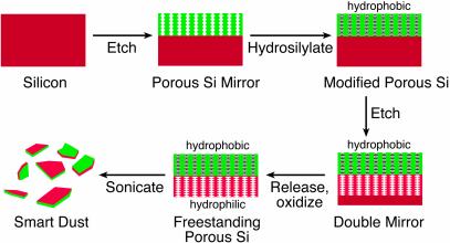
The present work represents an effort to use more complex building blocks with greater functionality as construction elements. Micrometer-sized one-dimensional photonic crystals of porous Si with optical spectra that change when they absorb chemicals are used. The method uses electrochemical etching and surface chemistry in tandem to prepare the nanostructured photonic crystals and a self-assembly mechanism resembling that by Mao et al. (13) to construct the sensor element at a targeted interface. The materials are prepared in two steps (as outlined in Fig. 1). In the first step, a one-dimensional photonic crystal is produced by electrochemically etching Si by using a time-varying electrical current. The second step involves chemically modifying the porous Si photonic structure. Steps 1 and 2 can be repeated on the same wafer, generating stratified porous Si photonic structures, the pore structure and chemical composition of which vary in a controlled fashion in the Si wafer. The films then are fractured into small particles, each particle containing in its nanostructure the necessary components to allow self-assembly, spectroscopic identification, and chemical sensing. Targeting and orientational order are imposed in the present work by interactions between the two chemically distinct faces of the photonic crystals at a liquid–liquid interface. Sensing is accomplished when liquid at the interface infuses into the porous mirrors, inducing predictable shifts in the optical spectra of both mirrors. Thus the microscopic photonic crystals spontaneously assemble, orient, and sense their local environment.
Fig. 1.
Scheme showing the synthesis of bifunctional smart-dust particles. A multilayered porous Si dielectric mirror (rugate filter) first is etched into the single-crystal Si substrate. The film then is hydrosilylated to generate a chemically stable hydrophobic mirror. A second rugate filter with a different periodicity is then etched into the substrate immediately beneath the first. The entire structure is removed from the Si substrate by the application of a current pulse. Thermal oxidation then imparts hydrophilic character to the second mirror. The bifunctional, freestanding film then is placed in water and fractured into micrometer-sized particles by ultrasonication.
Materials and Methods
The synthetic scheme followed to produce self-assembling and self-organizing bifunctional particles of porous Si photonic crystals is described in Fig. 1. A multilayered porous Si dielectric mirror first is electrochemically etched into the single-crystal Si (100) substrate (degenerate p type, B-doped, <1 mΩ–cm resistivity, obtained from Siltronix, Geneva). The etching solution consists of a 1:3 by volume mixture of absolute ethanol (Aldrich Chemicals) and aqueous 49% HF (Quantum Chemicals, Aukland, New Zealand). Etching is carried out in a Teflon cell by using a two-electrode configuration with a Pt mesh counter electrode. A sinusoidal current density waveform varying between 11.5 and 34.6 mA/cm2 is applied for 100 cycles and a periodicity of 7 s (14, 15). This side of the porous mirror is then thermally hydrosilylated with 1-dodecene following published procedures (16, 17). The second mirror is then prepared by placing the sample back in the Teflon etch cell and applying a sinusoidal current density varying between 11.5 and 34.6 mA/cm2, with 100 repeats and a periodicity of 8.7 s. The entire structure is then removed from the Si substrate by application of a current density pulse of 15.4 mA/cm2 for 45 s in an ethanol solution that is 3.3% by weight aqueous HF. The freestanding film is then placed in an oven in air at 100°C for 15 h. This step preferentially produces a thermal oxide on the more reactive, hydrogen-terminated freshly etched layer. For the small-particle studies the film is broken into micrometer-sized particles by ultrasonication as described (18).
Results and Discussion
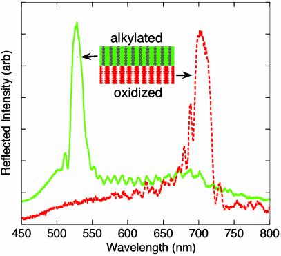
Porous Si prepared by using a sinusoidal current density waveform possesses an approximately sinusoidal porosity gradient in the direction of pore propagation (normal to the wafer surface in the present work). The porosity gradient results in a periodic variation in refractive index in the film. This structure, generally referred to as a rugate filter (19), produces a sharp diffraction feature in the optical reflectivity spectrum of the film (Fig. 2). The wavelength of the reflectivity maximum is determined by the periodicity and amplitude of the current waveform used in the etch (18).
Fig. 2.
Reflectivity spectra of a bifunctional porous Si rugate film. The green solid trace is obtained from the side of the film that contained a mirror etched by using a sinusoidal current varying between 11.5 and 34.6 mA/cm2. This side of the porous mirror then was hydrosilylated with 1-dodecene. The red dashed trace is obtained from the side of the film that contained a second mirror, etched by using a sinusoidal current varying between 11.5 and 34.6 mA/cm2 and then removed from the Si substrate. This side of the porous mirror was thermally oxidized. The total thickness of the porous Si film is ≈100 μm. The optical reflectivity spectra were obtained by using an Ocean Optics SD2000 charge-coupled device spectrometer fitted with focusing optics and by using tungsten light illumination. arb, arbitrary.
The procedure used to generate the chemically and optically asymmetric photonic structures used in this work is outlined in Fig. 1. A single rugate filter is first prepared. This film then is thermally hydrosilylated with dodecene following published procedures (16, 17), generating a chemically stable hydrophobic mirror. A second rugate filter with a different periodicity is then etched into the substrate immediately beneath the first. The oxide imparts hydrophilic character to the second mirror while the hydrosilylated side retains its hydrophobic nature, as determined by contact angle measurements (advancing contact angle with water: hydrophobic side, 92°; hydrophilic side, 39°). The chemical nature of the two faces is confirmed by diffuse reflectance infrared spectroscopy (Fig. 6, which is published as supporting information on the PNAS web site, www.pnas.org); absorption bands characteristic of aliphatic C—H vibrational modes (2,960–2,850 and 1,470 cm–1) are observed from the hydrosilylated side and a prominent band assigned to Si—O stretching (1,054 cm–1) is observed after oxidation.
The tandem etch/modify method described above provides a general means for producing optical films with spatially resolved, chemically distinct layers. The main requirement of the chemical modification reactions is that they be stable to the hydrofluoric acid etchant used in generating subsequent porous Si layers. It is anticipated that a number of chemical and electrochemical modification strategies developed for porous Si can be used with this procedure (20–22).
The bifunctional films will orient spontaneously at the surface of water, with the hydrophobic side facing up. If a small (≈2-mm on an edge) piece of the film floating on a water surface is picked up with forceps and flipped over, it will right itself spontaneously. The phenomenon is easily observed with the unaided eye due to the significant color difference between the hydrophobic and hydrophilic mirrors (green vs. red, respectively, in the present study). The addition of a hydrophobic liquid that is immiscible with water (such as heptane) to the water layer causes the films to localize at the liquid–liquid interface, with the hydrophobic mirror facing the hydrophobic liquid phase.
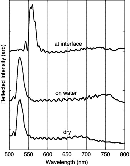
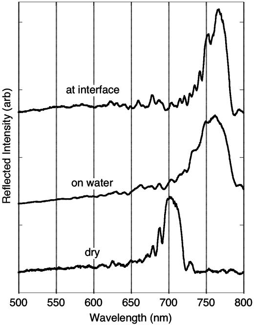
The reflectivity spectrum from the bifunctional mirrors provides a signal that reports on the interfacial interaction. The position of the spectral peaks in porous Si dielectric mirrors is a strong function of the average refractive index of the layers, and shifts in the photonic features have been shown to provide a very sensitive transduction modality for sensing of condensable vapors (23, 24), proteins (25, 26), DNA, and other molecules that can enter the pores (23, 25–28). In this work, the hydrosilylated layer is designed to display a spectral wavelength maximum of 530 nm in air. Liquid water will not infiltrate the hydrophobic pores, and the peak displays no discernable shift when the film is in contact with water (Fig. 3, “on water”). By contrast, in the presence of the heptane phase, the spectral feature shifts to 560 nm (Fig. 3, “at interface”). The complementary effect is observed on the opposite side of the film. In the present study the hydrophilic mirror displays a wavelength maximum of 702 nm (Fig. 4, “dry”); in contact with water the main spectral feature shifts to 762 nm (Fig. 4, “on water”). Subsequent addition of heptane to form the two-phase mixture does not shift this peak significantly (to 767 nm, Fig. 4, “at interface”).
Fig. 3.
Reflectivity spectra of the hydrophobic (alkylated) side of the bifunctional porous Si film from Fig. 2. The bottom trace (“dry”) is the same data represented by the solid line in Fig. 2 obtained with the sample in air. The “on water” trace represents the spectrum of the hydrophobic side of the sample when it is floating on water (obtained by looking down on the sample from above). The “at interface” trace represents the spectrum of the sample sitting at the water–heptane interface (obtained by looking through the heptane phase). Spectra are offset along the y axis for clarity. arb, arbitrary.
Fig. 4.
Reflectivity spectra of the hydrophilic (oxidized) side of the bifunctional porous Si film from Fig. 2. The bottom trace (“dry”) is the same data represented by the dashed line in Fig. 2 obtained with the sample in air. The “on water” trace represents the spectrum of the hydrophilic side of the sample when it is floating on water (obtained by looking up at the sample through the water layer). The “at interface” trace represents the spectrum of the sample sitting at the water–heptane interface (obtained by looking through the water phase). Spectra are offset along the y axis for clarity. arb, arbitrary.
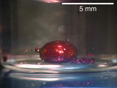
The same optical effects are observed on smaller [so-called smart-dust (14, 18, 29)] particles made by fracture of porous Si films through ultrasonication. The bifunctional, freestanding film is placed in ethanol and fractured into micrometer-sized particles by ultrasonication. The particles are observed to spontaneously assemble and orient at the interface of a small drop of dichloromethane in water (Fig. 5 and Figs. 7 and 8, which are published as supporting information on the PNAS web site). Spectra similar to those observed with the larger (mm-sized) films (Figs. 3 and 4) are observed on the micrometer-sized particles as well (Fig. 7), confirming that self-orientation and self-assembly occur with the small particles. In this case it is very difficult to measure the reflectivity spectrum from an individual particle but quite simple to measure the spectrum from an ensemble of the particles once they have assembled and oriented at the interface. The targeted assembly process thus provides an important amplification function.
Fig. 5.
Optical photograph of the bifunctional porous Si smart-dust particles assembled at the interface of a small drop of dichloromethane in a vial of water. The particles contain a hydrophobic green mirror and a hydrophilic red mirror on opposite sides; the red mirror is presented to the viewer.
The chemically asymmetric smart-dust particles enable interesting applications in high-throughput screening, drug discovery, biomedical implants, information display, optical switching, and chemical and biological sensor fields. We have demonstrated the use of the chemically stratified materials as a self-assembling chemical sensor in this work. The chemically asymmetric particles spontaneously target and align themselves at an organic liquid–water interface with the hydrophobic side oriented toward the organic phase and the hydrophilic side toward the water. A characteristic shift in the optical spectra of both mirrors signals the arrival of the particle at the interface. With the appropriate recognition elements attached, these self-targeting and self-orienting materials may be applied to a variety of interesting problems. For example, the particles might be used to locate, identify, and/or destroy certain cell types in the body or they might be used to locate and identify pathogenic bacteria in food or drinking water. Several features of porous Si are useful in this regard: porous Si has been shown to be biocompatible, and it has been investigated as a component in resorbable drug-delivery systems; (30–34) the photonic features from the multilayers can be observed at a distance or through human tissue; (14, 30) and the porous layers can act as a sensitive biosensor for proteins or DNA (23, 25–28).
Supplementary Material
Acknowledgments
We thank Prof. Kris Pister (University of California, Berkeley), Prof. Erkki Ruoslahti (The Burnham Institute), Prof. Sangeeta Bhatia (University of California at San Diego), and Victor Navone for inspiring discussions. We acknowledge financial support from the National Science Foundation and Air Force Office of Scientific Research Grant F49620-02-1-0288. J.R.L. thanks the University of California at San Diego California Institute of Telecommunications and Information Technology for a graduate fellowship.
References
- 1.Xia, Y., Rogers, J. A., Paul, K. E. & Whitesides, G. M. (1999) Chem. Rev. (Washington, D.C.) 99, 1823–1848. [DOI] [PubMed] [Google Scholar]
- 2.Porter, M. D., Bright, T. B., Allara, D. L. & Chidsey, C. D. (1987) J. Am. Chem. Soc. 109, 3559–3568. [Google Scholar]
- 3.Shelekhina, V. M., Prokhorov, O. A., Vityaz, P. A., Stupak, A. P., Gaponenko, S. V. & Gaponenko, N. V. (2001) Synth. Met. 124, 137–139. [Google Scholar]
- 4.Wijnhoven, J. E. G. J. & Vos, W. L. (1998) Science 281, 802–804. [DOI] [PubMed] [Google Scholar]
- 5.Xu, X., Majetich, S. A. & Asher, S. A. (2002) J. Am. Chem. Soc. 124, 13864–13868. [DOI] [PubMed] [Google Scholar]
- 6.Lee, K. & Asher, S. A. (2000) J. Am. Chem. Soc. 122, 9534–9537. [Google Scholar]
- 7.Park, S.-J., Lazarides, A. A., Mirkin, C. A. & Letsinger, R. L. (2001) Angew. Chem. Int. Ed. Engl. 40, 2909–2912. [PubMed] [Google Scholar]
- 8.Gerion, D., Parak, W. J., Williams, S. C., Zanchet, D., Micheel, C. M. & Alivisatos, A. P. (2002) J. Am. Chem. Soc. 124, 7070–7074. [DOI] [PubMed] [Google Scholar]
- 9.Loweth, C. J., Caldwell, W. B., Peng, X., Alivisatos, A. P. & Schultz, P. G. (1999) Angew. Chem. Int. Ed. Engl. 38, 1808–1812. [DOI] [PubMed] [Google Scholar]
- 10.Murray, C. B., Kagan, C. R. & Bawendi, M. G. (1995) Science 270, 1335–1338. [Google Scholar]
- 11.Collier, C. P., Vossmeyer, T. & Heath, J. R. (1998) Annu. Rev. Phys. Chem. 49, 371–404. [DOI] [PubMed] [Google Scholar]
- 12.Mirkin, C. A., Letsinger, R. L., Mucic, R. C. & Storhoff, J. J. (1996) Nature 382, 607–609. [DOI] [PubMed] [Google Scholar]
- 13.Mao, C., Thalladi, V. R., Wolfe, D. B., Whitesides, S. & Whitesides, G. M. (2002) J. Am. Chem. Soc. 124, 14508–14509. [DOI] [PubMed] [Google Scholar]
- 14.Schmedake, T. A., Cunin, F., Link, J. R. & Sailor, M. J. (2002) Adv. Mater. 14, 1270–1272. [Google Scholar]
- 15.Vincent, G. (1994) Appl. Phys. Lett. 64, 2367–2369. [Google Scholar]
- 16.Stewart, M. P. & Buriak, J. M. (1998) Angew. Chem. Int. Ed. Engl. 37, 3257–3260. [DOI] [PubMed] [Google Scholar]
- 17.Boukherroub, R., Wojtyk, J. T. C., Wayner, D. D. M. & Lockwood, D. J. (2002) J. Electrochem. Soc. 149, 59–63. [Google Scholar]
- 18.Cunin, F., Schmedake, T. A., Link, J. R., Li, Y. Y., Koh, J., Bhatia, S. N. & Sailor, M. J. (2002) Nat. Mater. 1, 39–41. [DOI] [PubMed] [Google Scholar]
- 19.Berger, M. G., Arens-Fischer, R., Thoenissen, M., Krueger, M., Billat, S., Lueth, H., Hilbrich, S., Theiss, W. & Grosse, P. (1997) Thin Solid Films 297, 237–240. [Google Scholar]
- 20.Dubois, T., Ozanam, F. & Chazalviel, J.-N. (1997) in Proceedings of the Electrochemical Society, eds. Schmuki, P., Lockwood, D. J., Isaacs, H. & Bsiesy, A. (Electrochemical Society, Pennington, NJ), Vol. 97-7, pp. 296–311. [Google Scholar]
- 21.Gurtner, C., Wun, A. W. & Sailor, M. J. (1999) Angew. Chem. Int. Ed. Engl. 38, 1966–1968. [DOI] [PubMed] [Google Scholar]
- 22.Buriak, J. M. (2002) Chem. Rev. (Washington, D.C.) 102, 1272–1308. [Google Scholar]
- 23.Snow, P. A., Squire, E. K., Russell, P. S. J. & Canham, L. T. (1999) J. Appl. Phys. 86, 1781–1784. [Google Scholar]
- 24.Gao, T., Gao, J. & Sailor, M. J. (2002) Langmuir 18, 9953–9957. [Google Scholar]
- 25.Arwin, H., Gavutis, M., Gustafsson, J., Schultzberg, M., Zangooie, S. & Tengvall, P. (2000) Phys. Status Solidi A 182, 515–520. [Google Scholar]
- 26.Collins, B. E., Dancil, K.-P., Abbi, G. & Sailor, M. J. (2002) Adv. Funct. Mat. 12, 187–191. [Google Scholar]
- 27.Chan, S., Horner, S. R., Miller, B. L. & Fauchet, P. M. (2001) J. Am. Chem. Soc. 123, 11797–11798. [DOI] [PubMed] [Google Scholar]
- 28.Sailor, M. J. (1997) in Properties of Porous Silicon, ed. Canham, L. (Short Run, London), Vol. 18, pp. 364–370. [Google Scholar]
- 29.Warneke, B., Last, M., Liebowitz, B. & Pister, K. S. J. (2001) Computer 34, 44–51. [Google Scholar]
- 30.Li, Y. Y., Cunin, F., Link, J. R., Gao, T., Betts, R. E., Reiver, S. H., Chin, V., Bhatia, S. N. & Sailor, M. J. (2003) Science 299, 2045–2047. [DOI] [PubMed] [Google Scholar]
- 31.Canham, L. T., Reeves, C. L., Loni, A., Houlton, M. R., Newey, J. P., Simons, A. J. & Cox, T. I. (1997) Thin Solid Films 297, 304–307. [Google Scholar]
- 32.Canham, L. T., Stewart, M. P., Buriak, J. M., Reeves, C. L., Anderson, M., Squire, E. K., Allcock, P. & Snow, P. A. (2000) Phys. Status Solidi A 182, 521–525. [Google Scholar]
- 33.Mayne, A. H., Bayliss, S. C., Barr, P., Tobin, M. & Buckberry, L. D. (2000) Phys. Status Solidi A 182, 505–513. [Google Scholar]
- 34.Canham, L. T. (1995) Adv. Mater. 7, 1033–1037. [Google Scholar]
Associated Data
This section collects any data citations, data availability statements, or supplementary materials included in this article.


