Abstract
We present detailed experimental and theoretical studies of the mechanics of thin buckled films on compliant substrates. In particular, accurate measurements of the wavelengths and amplitudes in structures that consist of thin, single-crystal ribbons of silicon covalently bonded to elastomeric substrates of poly(dimethylsiloxane) reveal responses that include wavelengths that change in an approximately linear fashion with strain in the substrate, for all values of strain above the critical strain for buckling. Theoretical reexamination of this system yields analytical models that can explain these and other experimental observations at a quantitative level. We show that the resulting mechanics has many features in common with that of a simple accordion bellows. These results have relevance to the many emerging applications of controlled buckling structures in stretchable electronics, microelectromechanical systems, thin-film metrology, optical devices, and others.
Keywords: buckling, stiff thin film, compliant substrate, stretchable electronics
Nonlinear buckling of thin, high modulus plates on compliant supports represents a classic problem in mechanics. Over the last several decades, numerous theoretical and experimental studies of this phenomenon have been performed (1–17). Although buckling has historically been viewed as a mechanism for structural failure, pioneering work in the late 1990s (18) showed that this behavior can be controlled in micro- and nanoscale systems to generate interesting structures with well defined geometries and dimensions in the 100 nm to 100 μm range. These observations created renewed interest in this area that persists today, with many active research groups currently exploring basic scientific aspects as well as applications in stretchable electronics (10–14, 19), micro- and nanoelectromechanical systems (MEMS and NEMS) (20), tunable phase optics (1, 21), force spectroscopy in cells (22), biocompatible topographic matrices for cell alignment (23, 24), high-precision micro- and nanometrology methods (15–17, 25), and pattern formation for micro/nanofabrication (18, 26–31). In these systems, controlled buckling is realized in thin films deposited, typically by vapor phase or physical transfer processes, onto prestrained elastomeric substrates. The prestrain is usually generated by one of two methods. The first involves thermally expanded elastomeric substrates, where the strains are on the order of a few percent (1, 10, 15–17). Depositing a film onto a heated substrate and then cooling the system lead to compressive strains in the film when its coefficient of thermal expansion is smaller than that of the substrate. Sufficiently large compression leads to buckling instabilities in the film that create “wavy” deformations (i.e., periodic, out-of-plane displacements of the film and surface region of the substrate). The second method uses mechanically stretched elastomeric substrates where the strain associated with the stretching (i.e., the prestrain) can range from a fraction of a percent to a few tens (1, 19) and even a few hundreds of a percent (32). Depositing a film on this stretched substrate and then releasing the prestrain can create wavy structures. The designs of these systems can range from simple layouts consisting of uniform films on flat substrates (16, 18, 21) to complex lithographically patterned films on substrates with structures of relief embossed on their surfaces (18, 33, 34). The diversity of wavy geometries enabled by these strategies creates considerable engineering flexibility in the types of structures that can be formed. A fundamental understanding of the physics is important because it can provide a foundation for developing routes to exploit this behavior in fields ranging from biology to nanoscale metrology to unusual electronics.
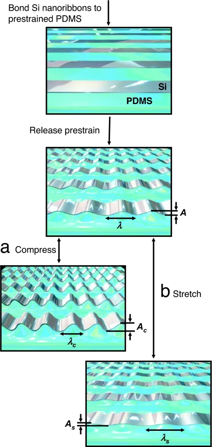
This article focuses on a class of system whose fabrication is illustrated in Fig. 1, although the basic theoretical considerations apply to all related systems in which buckling occurs. Here, thin ribbons of single-crystal semiconductors derived from high-quality wafer-based sources of material are chemically bonded to flat, prestrained elastomeric substrates of poly(dimethylsiloxane) (PDMS) (10). Releasing the prestrain leads to compressive strains on the ribbons that generate the wavy layouts. Applying strains to these structures and observing them with high-resolution microscopy techniques reveals the nature of their deformations and responses to strain.
Fig. 1.
Schematic illustration of the process for fabricating buckled, or wavy, single-crystal Si ribbons (silver) on a PDMS (blue) substrate (upper two frames). The lower two frames illustrate the response of these structures to strains applied to the PDMS.
Structures like those in Fig. 1 are of interest for applications in electronics. In particular, wavy electronic materials, such as the single-crystal inorganic semiconductors of Fig. 1 (10) or polycrystalline films of evaporated metals (11–14, 18, 19), provide fully reversible mechanical stretchability in electronic interconnects (11–14, 19) or in the active devices themselves, including metal-oxide field effect transistors (MOSFETs) (10), metal-semiconductor field effect transistors (MESFETs) (35), p–n junction diodes (10), and Schottky diodes (36). Integrated electronics that use such components could be important for devices such as flexible displays (37), eye-like digital cameras (38), comformable skin sensors (39), intelligent surgical gloves (40), and structural health monitoring devices (41). Besides their potential role in these applications, wavy single-crystal inorganic films provide valuable testbeds for examining the basic mechanics of the buckling process and the mechanical response of the wavy structures to applied strains. Unlike the related and more thoroughly studied cases of amorphous or polycrystalline films, high-purity single-crystal materials can be designed with dimensions (i.e., thicknesses, widths, and lengths) and mechanical properties (i.e., Young's modulus and Poisson ratio) that are extremely well controlled. Recent methods have been developed to allow the integration of defect-free single-crystal films with elastomeric substrates (10). These techniques enable systematic and repeatable studies of the buckling mechanics, to a precision that was not possible in previously studied systems. This article presents results of experiments that demonstrate the fundamental aspects of the buckling process. Theoretical reexamination of this classical problem leads to an analytical mechanics theory that provides a coherent and quantitatively accurate picture of the mechanics, which has direct connections to simple mechanics of an accordion bellows. Some implications of these findings on applications of buckled systems in electronics are presented.
Results and Discussion
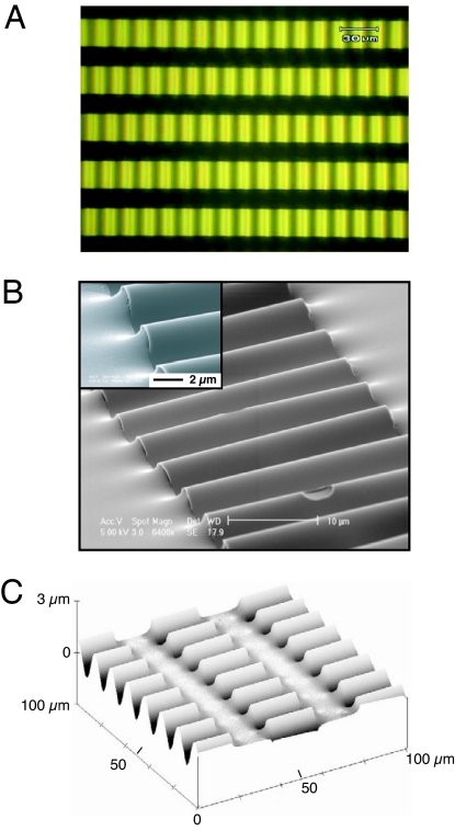
Fig. 2 shows optical, scanning electron, and atomic force micrographs of structures similar to those schematically illustrated in Fig. 1. Silicon-on-insulator (SOI) substrates or epitaxial layers on bulk wafers provided sources of high-quality single-crystal films with semiconductor device-grade levels of materials purity, uniformity in thickness (less than ±3%), and mechanical properties. Manipulating the surface chemistry of the ribbons created from these layers and the PDMS substrates enables covalent interfacial bonds to form between these two materials upon physical contact. In particular, silane coupling reactions between hydroxyl groups on the native oxide surfaces of Si ribbons and UV/ozone activated surfaces of the PDMS lead to exceptionally strong adhesion (42) and intimate mechanical coupling, as illustrated in the images of Fig. 2. In fact, the failure modes under extreme strains are cohesive in the ribbons (i.e., the ribbons crack) or the PDMS (i.e., the PDMS tears); adhesive failures at the interfaces are not observed. Wavy structures formed in this manner are highly sinusoidal (Fig. 2), with excellent uniformity in the amplitudes (less than ±5%) and wavelengths (less than ±3%) over large areas (up to 15 mm × 15 mm). Precision mechanical stages provide accurate means for applying strain to these structures. In situ scanning electron, optical, and atomic force microscopy can be used to quantify the mechanical responses.
Fig. 2.
Optical (A), scanning electron (B), and atomic force (C) micrographs of wavy, single-crystal Si ribbons. For A and C, 20-μm-wide and 100-nm-thick Si ribbons were used with PDMS prestrained to ≈28% for A and ≈23% for C. For B, 30-μm-wide, 150-μm-long, and 100-nm-thick Si ribbons were used with a PDMS prestrain of ≈15%.
Several mechanics models have been developed for buckling in composite structures of this type. Unlike classical column buckling analyses (e.g., ref. 43 and 44) that focus on the buckling load, these models describe results in terms of the wavelength and amplitude of the wavy structures. These dimensions are important in the emerging applications mentioned previously. Such models, whose range of applicability lies in the small deformation limit, all lead to the following predictions. For a thin film of thickness h and elastic modulus Ef on a prestretched substrate (prestrain, εpre) of modulus Es, releasing the prestrain leads to purely sinusoidal displacement distributions with wavelengths of (2–9, 45–47)
This equation predicts that the wavelength depends only on the film thickness and the film/substrate modulus ratio, and not on the prestrain εpre. The amplitude for the buckling process is given by (8)
 |
where
is defined as the critical buckling strain, or the minimum strain needed to induce buckling.
Because of the small deformation approximations and linear stress–strain behavior used to derive Eqs. 1 and 2, these results apply not only to the buckling process itself, but also to the response of the buckled system to applied strains, εapplied, by εpre − εapplied. In other words, Eq. 1 suggests not only that the buckling wavelength is independent of prestrain, but also that this wavelength will not change with strain (tensile or compressive) applied (εapplied) to the system after formation of the buckled structure, provided that the total strain (εpre − εapplied) is larger than εc. Eq. 2 can be used to describe this postbuckling behavior by simply replacing εpre by εpre − εapplied.
Eqs. 1 and 2 imply displacements that are tangential to the local surface relief, yielding a displacement trajectory that has the shape of a wave whose wavelength is fixed. The prestrain-independent wavelength in Eq. 1 and, by implication, the wavy motion trajectory have been widely applied to many experimental systems, with some level of qualitative or, in some cases, claimed quantitative agreement. These previous studies do not, however, provide sufficient precision to test rigorously the predictions of Eqs. 1 and 2 because they involve experimental uncertainties due to some combination of factors including poorly defined film/substrate interfaces, unknown mechanical properties in the films or substrates, poor spatial uniformity in the critical dimensions and mechanical properties, and/or the formation of micro- or nanocracks during film deposition or strain relaxation. The system of Figs. 1 and 2 avoids these limitations because of the highly controlled nature of the single-crystal films and the strong bonding to the elastomeric supports.
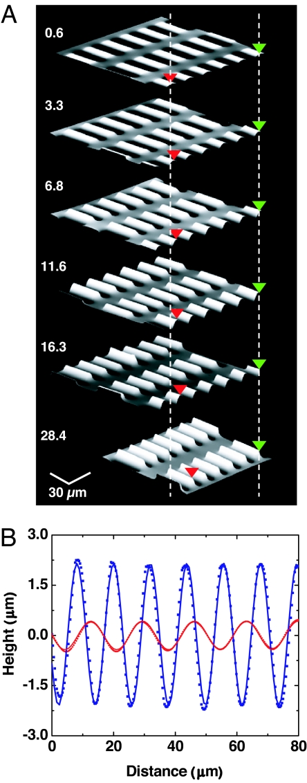
The most direct experimental test of the existing models involves the measurement of wavelengths in the well controlled systems of Figs. 1 and 2 at various εpre. All strains, for this case and the others that follow, were determined from the measured contour λcontour and wavelengths λ of the buckled ribbons and given by (λcontour − λ)/λ. Fig. 3 shows the results for the case of ribbons of single-crystal silicon with thicknesses of 100 nm on PDMS. The mean wavelength, ≈15 μm, is comparable to λo (≈18 μm) evaluated by using Eq. 1 with literature values for the mechanical properties (Ef = 130 GPa, Es = 1.8 MPa, vf = 0.27, vs = 0.48) (25, 48). The measurements show, however, a qualitative behavior characterized by a clear and systematic decrease in wavelength with increasing prestrain, contrary to the prediction of Eq. 1. Hints of similar variations in wavelength have also been reported for layers of polystyrene on PDMS substrates when the prestrain varies from ≈0% to 10% (1), and in platinum films on rubber substrates for prestrains of ≈400% (32). This strain-dependent wavelength behavior has also been observed in postbuckling studies of single-crystal Si and GaAs ribbons in the layouts of Figs. 1 and 2, where the wavelength varies systematically and in linear proportion to the applied strains (10, 49). These discrepancies between existing theory and experiments have been attributed to various effects, including nonlinearities in the stress–strain responses of the film or substrate materials (1), partial delamination of the films from the substrates, and finite size effects in the films (10). Detailed experimental studies indicate, however, that none of these explanations is valid for the case of the single-crystal systems of the type presented here. First, nonlinearities in the stress–strain behavior of the materials might be expected to lead to nonsinusoidal displacement profiles in the wavy structures, in contrast to the highly sinusoidal behavior observed in experiment, such as that shown in Fig. 3. In addition, independent measurements show that the elastic modulus of PDMS is constant, to a good approximation, for strains of up to several tens of a percent (50). Silicon and gallium arsenide single crystals exhibit linear responses up to strains that approach the fracture point (51). Second, detailed imaging studies such as those in Fig. 2 show that bonding in well designed systems can be extremely good. Third, finite size effects are likely unimportant because qualitatively similar variations in wavelength are observed in systems with ribbon widths between 2 and 100 μm, with thicknesses between 20 and 320 nm, with lengths between 5 and 15 mm, and on substrates with thicknesses between 0.5 and 5 mm.
Fig. 3.
The wavelength decreases as the prestrain increases, and the behavior of the buckled thin film is highly sinusoidal. (A) Atomic force micrographs of buckled Si ribbons (100 nm thickness) on PDMS, formed with various prestrains (indicated on the left in percent). The red and green triangles and the vertical dashed lines define particular relative locations on the samples, to illustrate more clearly the changes. The wavelength systematically decreases as the prestrain εpre increases. (B) Line cut profiles of a representative ribbon for the cases of εpre = 28.4% (blue) and εpre = 0.6% (red). The symbols are measured data; the lines are sinusoidal fits.
In the following, we present a buckling theory that accounts for finite deformations and geometrical nonlinearities to yield a quantitatively accurate description of the system. This buckling theory is different from previous models in the following three important aspects:
The initial strain-free (or stress-free) configurations for the substrate and film are different (i.e., the film is free of strain in the top frame of Fig. 1, whereas the substrate is free of strain in the second frame of Fig. 1, except near the film–substrate interface).
The strain-displacement relation in the substrate (as well as the film) is nonlinear.
The stress–strain relation in the substrate is characterized by the nonlinear neo-Hookean constitutive law.
Some details of this analysis, with derivations of expressions for the wavelengths and amplitudes of the wavy structures, appear in Materials and Methods.
Wavelength and Amplitude in Initial Buckling.
As with the previous analyses, the new theory predicts purely sinusoidal buckling displacements when the prestrain, εpre, exceeds the critical strain, εc. The wavelength, however, is different from that given by existing theories and can be written
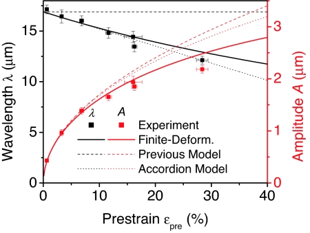
where λ0 is the wavelength in Eq. 1 and ξ = 5εpre(1 + εpre)/32. As shown in Fig. 4, λ depends on prestrain and quantitatively agrees with the experimental data without any parameter fitting, when the following values are used for the film thickness and modulus and substrate modulus: h = 100 nm, Ef = 130 GPa, Es = 1.8 MPa, vf = 0.27, vs = 0.48. An intuitive understanding of Eq. 3 is as follows: λ0/(1 + εpre) represents the change of wavelength expected based on simple accordion bellows mechanics; 1/(1 + ξ)1/3, which depends only on prestrain, results from the geometrical nonlinearity (finite deformation) and nonlinear constitutive model. For small prestrain, the value of λ approaches λ0, although it retains the same functional variation with εpre down to prestrains arbitrarily close to σc. As compared with the geometrical nonlinearity, the constitutive model of the substrate plays a relatively minor role on the prestrain-dependent wavelength and amplitude. Other constitutive models (e.g., linear relation between the second Piola–Kirchhoff stress and Green strain) that have the same linear elastic properties give essentially the same prestrain dependence of the wavelength. For the prestrain εpre = 28.4%, the present model gives the wavelength 12.9 μm, which agrees satisfactorily with the experimentally measured wavelength 12.1 ± 0.4 μm. Without accounting for the geometrical nonlinearity, the wavelength would be 14.6 μm, which shows the dominant effect of geometrical nonlinearity at the large strain.
Fig. 4.
Wavelength and amplitude of buckled structures of Si (100 nm thickness) on PDMS as a function of the prestrain. The finite-deformation buckling theory yields wavelengths and amplitudes that both agree well with experiments. Also shown are results from previous mechanics models (i.e., small deformation limit) and the simple accordion model.
The amplitude, according to the finite deformation theory, is
where A0 is the amplitude in Eq. 2. As shown in Fig. 4, the amplitude given by the Eq. 4 expression agrees well with the experimental data, whereas the amplitude A0 clearly overestimates. Similar to Eq. 3, an intuitive understanding of Eq. 4 is as follows: represents the change of amplitude expected based on simple accordion bellows mechanics; 1/(1 + ξ)1/3, which depends only on prestrain, results from the geometrical nonlinearity and nonlinear constitutive model in the substrate.
Membrane and Peak Strains in the Thin Film.
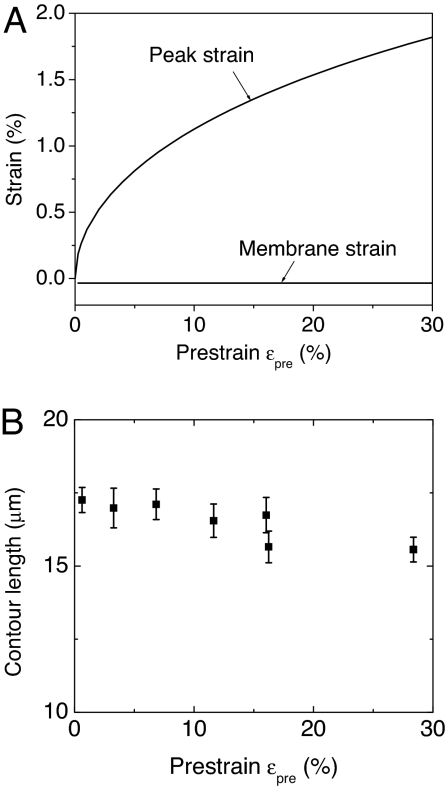
The new theory and the accuracy with which it reproduces experimental observation provide opportunities to reexamine the nature of strains and displacements in buckled systems. For εpre < εc (= 0.034% for the Si/PDMS system), relaxing the prestrain does not lead to buckling. Instead, the film supports small compressive strain (<0) that is very close to −εpre, which we refer to as membrane strain. When εpre > εc, the film buckles to relieve some of the strain; the membrane strain, εmem, as evaluated at the plane that lies at the midpoint of the thickness of the film, remains and has a magnitude almost equal to −εc. The peak strains εpeak in the film are equal to the sum of membrane strain εmem and the strain induced by the buckled geometry. In most cases of practical interest, the strain associated with the buckled geometry is much larger than εmem, thus this peak strain can be written
 |
The magnitude of εpeak is typically much smaller than the overall strain, εpre − εmem, that the film accommodates by buckling. For example, in the case of εpre = 28%, εpeak is only 1.8% for the system of Fig. 2. This mechanical advantage provides an effective level of stretchability/compressibility in materials that are intrinsically brittle. As a result, εpeak determines the point at which fracture occurs in the film. For Si, the fracture strain is in the range of εfracture (for either compression or tension). The maximum allowable prestrain is, therefore, approximately
which, for the system examined here, is ≈37% or almost 20 times larger than εfracture.
Fig. 5A shows the εpeak and εmem as a function of εpre. The membrane strain is negligible compared with the peak strain. Likewise, the peak strain is much smaller than the prestrain, such that the system can accommodate large strains. The measured contour length of the buckled Si film on PDMS substrate, shown in Fig. 5B, is approximately constant and is independent of the prestrain. This result is consistent with a negligibly small value for εmem.
Fig. 5.
Strains and contour length of the buckled thin film. (A) Membrane and peak strain in the Si as a function of prestrain for a system of buckled Si ribbons (100 nm thickness) on a PDMS substrate. The membrane strain is a small and constant throughout this range. (B) Measured contour length of the buckled Si structures as a function of prestrain. The nearly constant contour length is consistent with a small membrane strain.
Postbuckling Behavior.
When the buckled system is subjected to an applied strain εapplied, the wavelength and amplitude become
 |
where ζ = 5(εpre − εapplied)(1 + εpre)/32. The amplitude A vanishes when the applied strain reaches the prestrain plus the critical strain εc. In this situation, the membrane strain is equal to −εc. Additional applied strain relaxes the membrane strain and then, ultimately, appears as tensile strain in the silicon up to the point of fracture. The peak strain in the film is
 |
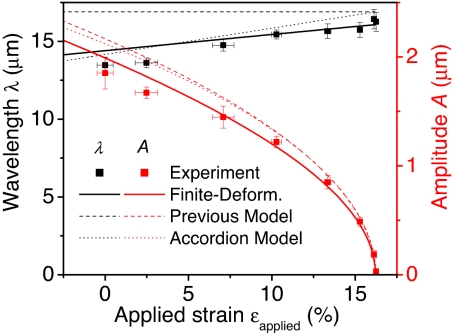
Fig. 6 gives the experimentally measured and theoretically predicted wavelength λ and amplitude A versus applied strain εapplied for a buckled Si thin-film/PDMS substrate formed with a prestrain of 16.2%, and other parameters the same as those of the examples described in the other sections. The constant wavelength and the amplitude predicted by the existing mechanics models, given by Eq. 2 with εpre replaced by εpre − εapplied, are also shown. The measured wavelength increases for tension and the measured amplitude decreases, reaching zero once the tensile strain reaches the prestrain. The finite-deformation buckling theory agrees well with experiments for both amplitude and wavelength. The existing mechanics models also capture the amplitude trend but deviate from the experimental results for large tensile strain (>10%).
Fig. 6.
Wavelength and amplitude of buckled structures of Si (100 nm thickness) on PDMS formed with a prestrain of 16.2%, as a function of the applied strain. The measured wavelength increases for tensile strain and the measured amplitude decreases, reaching zero once the tensile strain reaches the prestrain. The finite-deformation buckling theory yields wavelengths and amplitudes that both agree well with experiments. Results from previous mechanics models (i.e., small deformation limit) and the simple accordion model are also shown.
Comparison with Accordion Mechanics.
The finite deformation model introduced here captures quantitatively all of the experimental observations. A point of interest, however, is that the variations in amplitude and wavelength, with both prestrain and applied strain, can be captured with reasonable accuracy, for the systems studied here, with the very simple accordion model. In this model, the wavelength varies according to a simple rule of λ = λ0(1 − εpre + εapplied), where λ0 is the buckling wavelength at the onset of buckling given by Eq. 1. The value of λ0 cannot, of course, be determined with this accordion model, but it can be treated as a fitting parameter to describe experimentally measured data. For the amplitude, the accordion model assumes a constant contour length that provides an equation in integral form to compute the amplitude via
 |
Figs. 4 and 6 show the predicted variations in wavelength and amplitude with εpre and εapplied, based on this model. Although the results do not match exactly the experiment, the degree of agreement is remarkable, thereby indicating that the accordion picture of the mechanics of this system provides a good approximation of its qualitative behavior.
Conclusions
In summary, this work presents experimental data that reveal many details of the mechanical behavior of buckled thin films on compliant supports, with a focus on ribbons of single-crystal silicon on PDMS. Theoretical modeling, performed in a manner that removes certain approximations implemented in previous models of this class of system, quantitatively reproduces the observations. The results show that the structures behave, approximately, with the mechanics of an accordion bellows, in which strains are accommodated through changes in the amplitudes and the wavelengths of the buckled geometries. These conclusions and the detailed analyses are important for the many envisioned applications for buckled thin film/substrate systems.
Materials and Methods
Fabrication and Measurements.
The single-crystal Si (100) ribbons were derived from SOI wafers (SOItec), with top Si thicknesses between 20 and 300 nm. The first step in the fabrication involved patterning a layer of photoresist (AZ5214) in the geometry of the ribbons (2–100 μm wide, separated by 2–100 μm; 5–15 mm in length) on top of an SOI wafer using conventional photolithographic methods (Karl Suss MJB-3 contact mask aligner). Etching the exposed top Si layer by SF6 reactive ion etching (PlasmaTherm) defined the ribbons. Undercut etching of buried oxide layer with HF released the Si ribbons and left them resting on the underlying Si substrate. The PDMS (Sylgard 184; Dow) substrates were formed by casting and thermally curing (70°C for >4 h) a 10:1 (weight) mixture of base resin to crosslinking agent against a surface functionalized silicon wafer. Flat slabs of PDMS (0.5–5 mm thick) formed in this manner served as the substrates. Precision translation stages were used for stretching and compressing these substrates. The process for integrating the Si ribbons with the PDMS substrates began with exposure of the PDMS to UV (low-pressure mercury lamp, BHK, 173 μW/cm2 from 240 to 260 nm, at a distance of ≈10 mm) induced ozone for 1–3 min to create surface  OH groups, with the substrates in the stretching stage. Placing a processed SOI wafer against the PDMS and then removing the wafer transferred the Si ribbons to the PDMS through the action of strong, covalent
  O
O Si
Si O
O bonds that form at the interface. To avoid bonding between the PDMS and the silicon wafer of the SOI substrate (i.e., the handle wafer), the contact between the PDMS and the processed SOI was limited to ≈1 min. For this contact duration, the PDMS/Si adhesion was sufficiently strong that removing the PDMS lifted the Si ribbons from the Si handle wafer but sufficiently weak that the PDMS did not stick to the exposed regions of the wafer. After peeling back the PDMS with the Si ribbons on its surface, the bonding was allowed to run to completion (>10 min at room temperature) before releasing or applying strains. The translation stage for controlling the strain was designed to fit into optical, scanning electron, and atomic force microscopes, for the purpose of in situ observation. Optical microscopy was used to determine the wavelength by measuring the distance between two points in the image and dividing by the number of waves in between. Atomic force microscopy (DI 3100; Veeco) was used to determine the amplitudes and to verify the wavelength measurements.
Analysis.
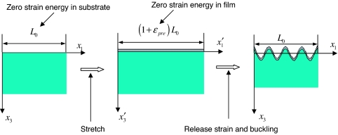
Fig. 7 defines the parameters and variables for three stages of controlled buckling in Fig. 1. Fig. 7 Left (stage I) illustrates the initial state of the PDMS before prestretching with original length L0, which represents its zero strain energy configuration. Fig. 7 Middle (stage II) shows the stretched PDMS attached to an undeformed Si film. After prestretching, the length of the PDMS is L0(1 + εpre), which is also the original length of the undeformed Si film. Fig. 7 Middle also gives the zero strain energy state of the Si. Relaxing the prestrain will buckle the Si film, as shown in Fig. 7 Right (stage III). The positions in the substrate in stage I (and III) are related to stage II by x′ = x(1 + εpre). The normal displacement on the substrate is w = A cos(2πx/λ). The thin-film membrane energy and bending energy per unit length can be obtained from the von Karman plate theory (52) and are given by
and
respectively. [Details are given in the supporting information (SI).] The total energy in the film is (Um + Ub)L0(1 + εpre), where L0(1 + εpre) is the film length at its strain-free stage.
Fig. 7.
Three sequential configurations for the thin film/substrate buckling process. (Left) Undeformed substrate with the original length L0, which represents the zero strain energy state. (Middle) Substrate deformed by the prestrain and the integrated film, which represents its zero strain energy state. (Right) Deformed (buckled) configuration.
The substrate is subjected to the surface displacement w = A cos(2πx/λ) and prestrain εpre. For large deformation, the Green strains EIJ in the substrate are related to the displacements u by (53) EIJ = (uI,J + uJ,I + uK,IuK,J). The stress–strain relation of polymer is nonlinear and is usually characterized by the neo-Hookean constitutive law for the second Piola–Kirchhoff stress TIJ and Green strain (53). The force equilibrium equations (53) are (TJKFiK),J = 0, where FiK is the deformation gradient.
The governing equations for the substrate become highly nonlinear. Because the amplitude A is much less than the wavelength λ, we identify A/λ as a small parameter and expand the displacement field to the order of A/λ, (A/λ)2 and (A/λ)3. For an incompressible substrate, the energy per unit length is Us = (π/3)Es(A2/λ)(1 + (5/32)(π2A2/λ2)). (Details are given in the SI.) Minimization of total energy per unit length, Utot = (Um + Ub)(1 + εpre) + Us, i.e., ∂Utot/∂A = ∂Utot/∂λ = 0 gives the wavelength and amplitude in Eqs. 3 and 4.
Supplementary Material
Acknowledgments
We thank J. Hanlon of the Beckman Institute for the images of Fig. 1 and T. Banks and K. Colravy for help with processing using facilities at the Frederick Seitz Materials Research Laboratory. This material is based on work supported by the National Science Foundation under Grant DMI-0328162 and the U.S. Department of Energy, Division of Materials Sciences, under Award DEFG02-91ER45439, through the Frederick Seitz Materials Research Laboratory and Center for Microanalysis of Materials at the University of Illinois at Urbana–Champaign. H.J. acknowledges the support from National Science Foundation Grant CMMI-0700440, and Y.H. acknowledges support from the National Natural Science Foundation of China.
Abbreviations
- PDMS
poly(dimethylsiloxane)
- SOI
silicon-on-insulator.
Footnotes
The authors declare no conflict of interest.
This article is a PNAS Direct Submission.
This article contains supporting information online at www.pnas.org/cgi/content/full/0702927104/DC1.
Ē = E/(1 − v2) is the plane-strain modulus, and v is the Poisson ratio.
References
- 1.Harrison C, Stafford CM, Zhang WH, Karim A. Appl Phys Lett. 2004;85:4016–4018. [Google Scholar]
- 2.Huang R. J Mech Phys Solids. 2005;53:63–89. [Google Scholar]
- 3.Huang R, Im SH. Phys Rev E. 2006;74:12. doi: 10.1103/PhysRevE.74.026214. [DOI] [PubMed] [Google Scholar]
- 4.Huang R, Suo Z. J Appl Phys. 2002;91:1135–1142. [Google Scholar]
- 5.Huang R, Suo Z. Int J Solids Struct. 2002;39:1791–1802. [Google Scholar]
- 6.Huang R, Yin H, Liang J, Sturm JC, Hobart KD, Suo Z. Acta Mech Sin. 2002;18:441–456. [Google Scholar]
- 7.Huang ZY, Hong W, Suo Z. Phys Rev E. 2004;70:4. doi: 10.1103/PhysRevE.70.030601. [DOI] [PubMed] [Google Scholar]
- 8.Huang ZY, Hong W, Suo Z. J Mech Phys Solids. 2005;53:2101–2118. [Google Scholar]
- 9.Im SH, Huang R. Acta Mater. 2004;52:3707–3719. [Google Scholar]
- 10.Khang DY, Jiang HQ, Huang Y, Rogers JA. Science. 2006;311:208–212. doi: 10.1126/science.1121401. [DOI] [PubMed] [Google Scholar]
- 11.Lacour SP, Jones J, Suo Z, Wagner S. IEEE Electron Device Lett. 2004;25:179–181. [Google Scholar]
- 12.Lacour SP, Jones J, Wagner S, Li T, Suo ZG. Proc IEEE. 2005;93:1459–1467. [Google Scholar]
- 13.Lacour SP, Wagner S, Huang ZY, Suo Z. Appl Phys Lett. 2003;82:2404–2406. [Google Scholar]
- 14.Lacour SP, Wagner S, Narayan RJ, Li T, Suo ZG. J Appl Phys. 2006;100 014913. [Google Scholar]
- 15.Stafford CM, Guo S, Harrison C, Chiang MYM. Rev Sci Instrum. 2005;76 062207. [Google Scholar]
- 16.Stafford CM, Harrison C, Beers KL, Karim A, Amis EJ, Vanlandingham MR, Kim HC, Volksen W, Miller RD, Simonyi EE. Nat Mater. 2004;3:545–550. doi: 10.1038/nmat1175. [DOI] [PubMed] [Google Scholar]
- 17.Stafford CM, Vogt BD, Harrison C, Julthongpiput D, Huang R. Macromolecules. 2006;39:5095–5099. [Google Scholar]
- 18.Bowden N, Brittain S, Evans AG, Hutchinson JW, Whitesides GM. Nature. 1998;393:146–149. [Google Scholar]
- 19.Wagner S, Lacour SP, Jones J, Hsu PHI, Sturm JC, Li T, Suo ZG. Physica E. 2004;25:326–334. [Google Scholar]
- 20.Fu YQ, Sanjabi S, Barber ZH, Clyne TW, Huang WM, Cai M, Luo JK, Flewitt AJ, Milne WI. Appl Phys Lett. 2006;89:171922. [Google Scholar]
- 21.Efimenko K, Rackaitis M, Manias E, Vaziri A, Mahadevan L, Genzer J. Nat Mater. 2005;4:293–297. doi: 10.1038/nmat1342. [DOI] [PubMed] [Google Scholar]
- 22.Harris AK, Wild P, Stopak D. Science. 1980;208:177–179. doi: 10.1126/science.6987736. [DOI] [PubMed] [Google Scholar]
- 23.Teixeira AI, Abrams GA, Bertics PJ, Murphy CJ, Nealey PF. J Cell Sci. 2003;116:1881–1892. doi: 10.1242/jcs.00383. [DOI] [PMC free article] [PubMed] [Google Scholar]
- 24.Jiang XY, Takayama S, Qian XP, Ostuni E, Wu HK, Bowden N, LeDuc P, Ingber DE, Whitesides GM. Langmuir. 2002;18:3273–3280. [Google Scholar]
- 25.Wilder EA, Guo S, Lin-Gibson S, Fasolka MJ, Stafford CM. Macromolecules. 2006;39:4138–4143. [Google Scholar]
- 26.Bowden N, Huck WTS, Paul KE, Whitesides GM. Appl Phys Lett. 1999;75:2557–2559. [Google Scholar]
- 27.Huck WTS, Bowden N, Onck P, Pardoen T, Hutchinson JW, Whitesides GM. Langmuir. 2000;16:3497–3501. [Google Scholar]
- 28.Sharp JS, Jones RAL. Adv Mater. 2002;14:799–802. [Google Scholar]
- 29.Yoo PJ, Suh KY, Park SY, Lee HH. Adv Mater. 2002;14:1383–1387. [Google Scholar]
- 30.Schmid H, Wolf H, Allenspach R, Riel H, Karg S, Michel B, Delamarche E. Adv Funct Mater. 2003;13:145–153. [Google Scholar]
- 31.Moon MW, Lee SH, Sun JY, Oh KH, Vaziri A, Hutchinson JW. Proc Natl Acad Sci USA. 2007;104:1130–1133. doi: 10.1073/pnas.0610654104. [DOI] [PMC free article] [PubMed] [Google Scholar]
- 32.Volynskii AL, Bazhenov S, Lebedeva OV, Bakeev NF. J Mater Sci. 2000;35:547–554. [Google Scholar]
- 33.Lee KJ, Motala MJ, Meitl MA, Childs WR, Menard E, Shim AK, Rogers JA, Nuzzo RG. Adv Mater. 2005;17:2332–2336. [Google Scholar]
- 34.Sun YG, Graff RA, Strano MS, Rogers JA. Small. 2005;1:1052–1057. doi: 10.1002/smll.200500094. [DOI] [PubMed] [Google Scholar]
- 35.Sun YG, Kim S, Adesida I, Rogers JA. Appl Phys Lett. 2005;87 083501. [Google Scholar]
- 36.Sun YG, Rogers JA. Nano Lett. 2004;4:1953–1959. [Google Scholar]
- 37.Crawford GP. Flexible Flat Panel Display Technology. New York: Wiley; 2005. [Google Scholar]
- 38.Jin HC, Abelson JR, Erhardt MK, Nuzzo RG. J Vac Sci Technol B. 2004;22:2548–2551. [Google Scholar]
- 39.Lumelsky V, Shur MS, Wagner S. IEEE Sensors J. 2001;1:41–51. [Google Scholar]
- 40.Someya T, Sekitani T, Iba S, Kato Y, Kawaguchi H, Sakurai T. Proc Natl Acad Sci USA. 2004;101:9966–9970. doi: 10.1073/pnas.0401918101. [DOI] [PMC free article] [PubMed] [Google Scholar]
- 41.Nathan A, Park B, Sazonov A, Tao S, Chan I, Servati P, Karim K, Charania T, Striakhilev D, Ma Q, et al. Microelectron J. 2000;31:883–891. [Google Scholar]
- 42.Childs WR, Nuzzo RG. J Am Chem Soc. 2002;124:13583–13596. doi: 10.1021/ja020942z. [DOI] [PubMed] [Google Scholar]
- 43.Goodier JN, Neou IM. J Aeronaut Sci. 1951;18:649–657. [Google Scholar]
- 44.Allen HG. Analysis and Design of Structural Sandwich Panels. Tarrytown, NY: Pergamon; 1969. [Google Scholar]
- 45.Im SH, Huang R. J Appl Mech Trans ASME. 2005;72:955–961. [Google Scholar]
- 46.Chen X, Hutchinson JW. J Appl Mech Trans ASME. 2004;71:597–603. [Google Scholar]
- 47.Groenewold J. Physica A. 2001;298:32–45. [Google Scholar]
- 48.Information Service in Physics, Electrotechnology, Computers and Control. Properties of Silicon. New York: Institution of Electrical Engineers; 1988. [Google Scholar]
- 49.Sun Y, Choi WM, Jiang H, Huang YY, Rogers JA. Nat Nanotechnol. 2006;1:201–207. doi: 10.1038/nnano.2006.131. [DOI] [PubMed] [Google Scholar]
- 50.Choi KM, Rogers JA. J Am Chem Soc. 2003;125:4060–4061. doi: 10.1021/ja029973k. [DOI] [PubMed] [Google Scholar]
- 51.Virwani K, Malshe A, Schmidt W, Sood D. Smart Mater Struct. 2003;12:1028–1032. [Google Scholar]
- 52.Timoshenko S, Gere J. Theory of Elastic Stability. New York: McGraw–Hill; 1961. [Google Scholar]
- 53.Symon K. Mechanics. Reading, MA: Addison–Wesley; 1971. [Google Scholar]
Associated Data
This section collects any data citations, data availability statements, or supplementary materials included in this article.


