Abstract
Background
In recent years scientists have been trying both to increase the efficiency of solar cells, whilst at the same time reducing dimensions and costs. Increases in efficiency have been brought about by implanting carbon nanotubes onto the surface of solar cells in order to reduce the reflection of sunrays, as well as through the insertion of polymeric arrays into the intrinsic layer for charge separation.
Results
The experimental results show power rising linearly for intrinsic layer thicknesses between 0–50 nm. Wider thicknesses increase the possibility of recombination of electrons and holes, leading to perturbation of the linear behaviour of output power. This effect is studied and formulated as a function of thickness. Recognition of the critical intrinsic layer thickness can permit one to determine the length of carbon nanotube necessary for optimizing solar cells.
Conclusion
In this study the behaviour of output power as a function of intrinsic layer thicknesses has been described physically and also simulated. In addition, the implantation of carbon nanotubes into the intrinsic layer and the necessary nanotube length required to optimize solar cells have been suggested.
Background
Developing inexpensive and renewable energy sources is one of the most important scientific and technological challenges of our time. Solar energy is an inexhaustible energy source that can be harnessed to meet our growing future energy needs. However, traditional photovoltaic (solar-to-electric conversion) technology is too expensive to be the suitable alternative for fossil fuels or even other competing renewable energy sources. A significant leap in the scientific and technological progress of renewable energy sources will be required to displace proven, but unsustainable energy production methods.
Nanotechnology is driving new interesting developments in photovoltaic technology. Advances in organic synthesis and characterization techniques allow us to coax a photocurrent from organic, 'soft' molecules in a process that mimics photosynthesis in plants, thus potentially opening up the way to cheap, ubiquitous solar cells. Power production resulting in zero greenhouse gas emissions is economically and environmentally desirable. Direct photovoltaic conversion of sunlight into electricity is therefore the highly attractive alternative to unsustainable energy sources such as fossil fuels.
Although silicon solar cells have gained a considerable market share and commercial success, high production and up-front installation costs still limit their commercial viability. In this study, we explore the use of low-cost advanced materials for photovoltaic energy production and the mechanism of photovoltaic action in a new class of solar cell, that is, the heterojunction photovoltaic. These are constructed from a thin film of cheap composite material, a mixture of carbon nanotubes and conductive polymer [1].
Results
We now aim to address the issues that determine the thickness of the absorber (or "intrinsic") layer. Figure 1 illustrates a computational calculation that shows how the output power of an a-Si-based pin cell varies with intrinsic layer thickness. The curves differ in the specified absorption coefficients for a monochromatic illumination using varying photon energies. All curves were calculated for the same photon flux. Such illumination conditions might be achieved by experiment using a laser whose photon energy can be tuned from 1.8 to 2.3 eV, however the presence of sunlight, of course, presents a much more complex situation.
Figure 1.
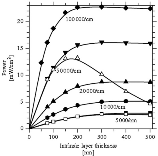
Computer calculation of the power output from a pin solar cell as a function of intrinsic layer thickness. The differing curves indicate results for monochromatic illumination with absorption coefficients from 5000/cm to 100 000/cm; for typical a-Si: H, this range corresponds to a photon energy range from 1.8 to 2.5 eV. Solid symbols indicate illumination through the p-layer and open symbols indicate illumination through the n-layer. Incident photon flux = 2 × 10¹⁷/cm2s; no back reflector. The data are obtained from real experiments, with the curves calculated using methods outlined in the references [3-8].
We will first discuss the results for illumination through the p-layer (solid symbols in the figure). For intrinsic layers that are sufficiently thin, the power is proportional to the number of photons absorbed (i.e. to the product of the thickness, d and the absorption coefficient, η). Within this limit the fill factors have nearly ideal values around 0.8. As the thickness of the cell increases, the power saturates. In figure 1 the first plot (η = 100 000/cm – corresponding photon energy of about 2.3 eV) shows the behaviour for strongly absorbed illumination. Power saturation occurs for thicknesses greater than 100 nm, that is, typical distance at which photons are absorbed. Since thicker cells do not absorb much additional light, going beyond this length means power stops increasing [2].
Model and objective
Different models have been proposed to simulate the experimental results [3-8]. Figure 1 shows the behaviour of power as a function of intrinsic layer thickness. Several experiments have been carried out to demonstrate the effect of layer thickness on output power.
As can be observed in figure 1, power grows linearly and becomes saturated after a distinct value of layer thickness. If we neglect recombination of electrons and holes, the output power can be expressed as:
| Pα = αw, |
where, α is a coefficient and can be calculated for each curve, w is the intrinsic layer thickness, with Pα termed the ideal power (linear form).
Because the recombination phenomena begin at a certain intrinsic layer thickness then it is useful to plot Pα-Pexp as a function of the intrinsic layer thickness. Figure 2 shows the difference between the experimental power and Pα as a function of the intrinsic layer for P1 type with α = 0.24 and η = 100 000/cm (absorption coefficients).
Figure 2.
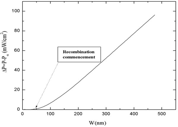
The difference between ideal (linear form) and experimental power as a function of the intrinsic layer thickness for P1 type.
On the basis of figure 2 we can produce an equation that contains the recombination phenomena as:
| P = Pα - β(w - wc)n, |
where β is the recombination coefficient. This equation is plotted in figure 3 with β = 0.02 and n = 1.41.
Figure 3.
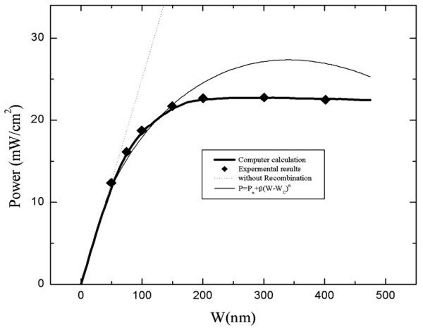
Ideal, theoretical and experimental power as a function of the intrinsic layer thickness for P1 type.
Figure 3 shows the ideal (linear form), theoretical and experimental powers as a function of the intrinsic layer thickness for P1 type. The recombination phenomena start at Wc = 40 nm, which we call the critical intrinsic layer.
From figure 3 it can be seen that the theoretical power values between 0–150 nm almost match the experimental results. However after 150 nm the agreement between the fits is poor. When the difference between the intrinsic layer thickness and carrier current cross section is small, the two-dimensional recombination phenomena are expected to dominate (from 40 nm up to 150 nm for P1 type). Whereas, when the difference between the intrinsic layer thickness and carrier current cross section is large (after 150 nm for P1 type) the three-dimensional recombination phenomena dominate. On increasing the length of intrinsic layer, the three-dimensional recombination becomes dominant and exhibits linear behaviour.
Therefore, the theoretical model plot can be defined by three regions that is, linear (0–40 nm), two-dimensional and three-dimensional recombination phenomena:
| P = αw - β(w - wc)n + (a - α'w), |
where a and α' are the three dimensional recombination coefficients.
Because of interference between two-dimensional and three-dimensional recombination terms in equation 3, this equation is not appropriate for simulation. Consequently we need to modify equation 3 thus:
| Pth = αw - β(|w - wc|)n X(w) + (a - α'w)Y(w), |
where X (w) is the creation and destruction function and Y (w) is the creation function.
We shall now define the function, starting fist with the destruction function,
where γ is function sharpness parameter.
Figure 4 shows the plot of the destruction function against different sharpness parameters.
Figure 4.
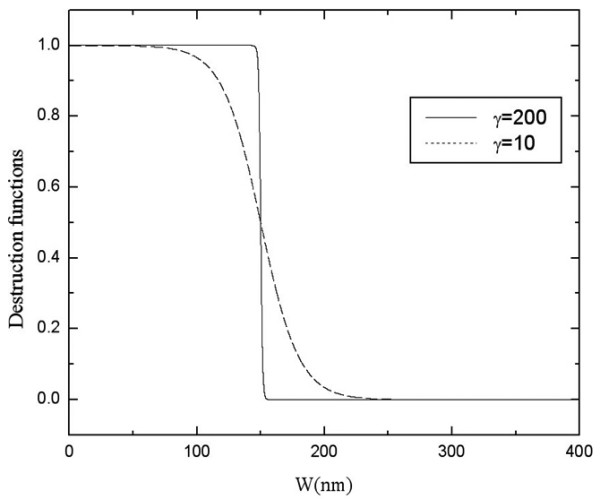
Destruction functions as a function of different sharpness parameters.
Second, the creation function can be defined as:
Lastly, we can express the creation and destruction function X(w) as:
The behaviour of equation 7 is shown in figure 5. We can calculate the data for the theoretical power plot by using the functions X (w), Y (w) and equation. 4. The data plotted for the calculation of theoretical power with a function sharpness parameter equal to 5 are shown in table 1. It is important to note that the recombination starts at wc. A plot using the data outlined in table 1 is shown in figure 6.
Figure 5.
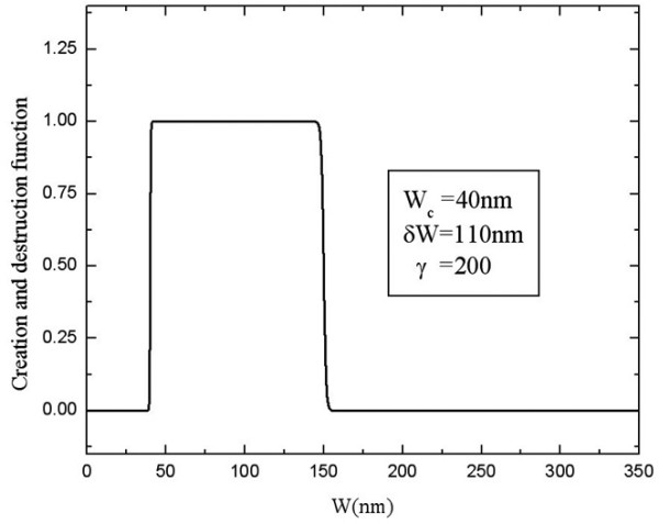
Creation and destruction function at different sharpness parameters.
Table 1.
Data plotted for the calculation of theoretical power (γ = 5).
| type | α | β | wc | n | δw | a | α' |
| P1 (100 000/cm) | 0. 24 | 0.02 | 40 | 1.41 | 120 | 22.71 | 0.2405 |
| P2 (50 000/cm) | 0.124 | 0.0011 | 55 | 1.85 | 140 | 17.3 | 0.1265 |
| P3 (20 000/cm) | 0.053 | 0.0004 | 70 | 1.85 | 170 | 8.96 | 0.053 |
| P4 (10 000/cm) | 0.024 | 0.000065 | 97 | 2.0105 | 230 | 6 | 0.0249 |
| P5 (5000/cm) | 0.0116 | 0.0000035 | 110 | 2.31 | 260 | 2.1 | 0.01 |
Figure 6.
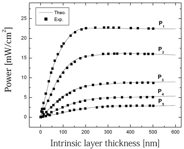
Simulated plot of power as a function of intrinsic layer thickness.
The necessary length of carbon nanotube for an optimized solar cell
Because of the symmetry and unique electronic structure of graphene, the nanotube's structure strongly affects its electrical properties. For a given (n, m) nanotube, if n – m is a multiple of 3, then the nanotube is metallic; such is the case for all armchair (n = m) nanotubes. In terms of metallic behaviour, carbon nanotubes can have conductivity up to eight times that of copper, and can carry a current density comparable to that of any known conventional metallic wire; this makes carbon nanotubes potential candidates as nanoscale wires [9]. It is consequently possible to reduce the recombination phenomena by using the carbon nanotubes in the intrinsic layer. The presence of an aligned doped carbon nanotube (armchair, superconducting) in the intrinsic layer helps maintain linear power generation behaviour, in addition to making solar cells with higher output powers.
It is necessary to know the proper length of doped carbon nanotubes as a function of intrinsic layer thickness. The non-linearity of power starts at wc, which for P1 type, for example, starts at 40 nm. So the necessary length of carbon nanotube for optimizing a solar cell, as a function of the intrinsic layer, can be expressed as:
| Lnanotube = w - wc |
It is important to note that the volume occupied by carbon nanotubes in the intrinsic layer affects only the linearity coefficient.
Conclusion
When considering the behaviour of power as a function of intrinsic layer thickness, the recombination of electrons and holes plays an important role in reducing the power. Eliminating recombination is useful in maintaining the linear behaviour of power and in producing solar cells with high powers. If the intrinsic layer thickness is comparable to the carrier current cross section, the two dimensional recombination phenomena are dominant; otherwise the three dimensional recombination phenomena would dominate. In this study, power as a function of the intrinsic layer thickness was simulated and plotted, thus allowing us to express the necessary length of carbon nanotubes required for optimized solar cells as a function of the intrinsic layer thickness.
Contributor Information
Majid Vaezzadeh, Email: majid@kntu.ac.ir.
Mohammad Reza Saeedi, Email: saidimohammadreza@yahoo.com.
Tirdad Barghi, Email: Tirdad.barghi@gmail.com.
Mohammad Reza Sadeghi, Email: babalengderazir@gmail.com.
References
- Motta N, Waclawik ER, Goh R, Bell JM. Nanotube-polymer Solar Cells – an Alternative to Silicon. Bollettino della Comunità Scientifica in Australasia. 2005. pp. 15–20.http://eprints.qut.edu.au
- Luque A, Hegedus S. John Wiley & Sons Handbook of Photovoltaic Science and Engineering. Ltd ISBN: 0-471-49196-9; 2003. [Google Scholar]
- Davis MarkW, Hunter Fanney A, Dougherty BrianP. Evaluating building integrated photovoltaic performance models. National Institute of Standards and Technology, Gaithersburg, MD 20899-8632.
- Dianove M, Kazansky PG, Stepanovd Yu. Acad Sci USSR. General physics inst., dep. fiber optics, Moscow 117942, URSS (Sov. lightwave commun.); Photovoltaic model of photoinduced second-harmonic generation in optical fibers. [Google Scholar]
- De Blas MA, Torres JL, Prieto E, Garca A. Selecting a suitable model for characterizing photovoltaic devices. Renewable Energy. 2002;25:371–380(10). doi: 10.1016/S0960-1481(01)00056-8. [DOI] [Google Scholar]
- Cristofari C, Poggi P, Notton G, Muselli M. Thermal Modelling of a Photovoltaic Module. Proceeding Modelling, Simulation, and Optimization. 2006;507 [Google Scholar]
- Hunter Fanney A, Dougherty BrianP, Davis MarkW. National Institute of Standards and Technology. 100 Bureau Drive, MS 8632, Gaithersburg, MD 20899-8632; 2002. Short-Term Characterization of Building Integrated Photovoltaic Panels. [Google Scholar]
- Munoz-Perez MA, Rodriguez-Pichardo A, Camacho Martinez F, Sidrach-de-Cardona M, Mora Lopez L. A simple model for sizing stand alone photovoltaic systems. Solar Energy Materials and Solar Cells. pp. 199–214(16). 24 August 1998.
- Appenzeller J, Martel R, Derycke V, Radosavljevic M, Wind S, Neumayer D, Avouris P. Carbon nanotubes as potential building blocks for future nanoelectronics. Microelectronic Engineering. 2002;64:391–7. doi: 10.1016/S0167-9317(02)00813-4. [DOI] [Google Scholar]


