

Abstract
A very high resolution small animal positron emission tomograph (PET) which can achieve sub-millimeter spatial resolution is being developed using silicon pad detectors. The prototype PET for a single slice instrument consists of two 1 mm thick silicon pad detectors, each containing a 32 × 16 array of 1.4 mm × 1.4 mm pads read out with four VATAGP3 chips which have 128 channels low-noise self triggering ASIC in each chip, coincidence units, a source turntable and tungsten slice collimator. The silicon detectors were located edgewise on opposite sides of a 4 cm field-of-view to maximize efficiency. Energy resolution is dominated by electronic noise, which is 0.98% (1.38 keV) FWHM at 140.5 keV. Coincidence timing resolution is 82.1 ns FWHM and coincidence efficiency was measured to be 1.04 × 10⁻³ % from two silicon detectors with annihilation photons of 18F source Image data were acquired and reconstructed using conventional 2-D filtered-back projection (FBP) and a maximum likelihood expectation maximization (ML-EM) method. Image resolution of approximately 1.45 mm FWHM is obtained from 1-D profile of 1.1 mm diameter 18F line source image. Even better resolution can be obtained with smaller detector element sizes. While many challenges remain in scaling up the instrument to useful efficiency including densely packed detectors and significantly improved timing resolution, performance of the test setup in terms of easily achieving submillimeter resolution is compelling.
Keywords: Very high resolution, Positron emission tomograph (PET), Silicon pad detector, VATAGP3 ASIC
1. Introduction
Biomedical research using animal models of metabolism and disease mechanisms demands a very high resolution animal PET system since mice and other small animals are frequently used as experimental animals. However, existing animal PET scanners consisting of scintillation detectors have a resolution limit 1-2 mm FWHM caused by positioning error due to Compton scatter, coherent scatter, and poor (or no) depth-of-interaction (DOI) resolution coupled with the penetrating nature of annihilation photons in detector elements. The microPET II scanner [1-2], current state-of-the-art PET scanner for animal imaging, was newly developed. The microPET II consisting of 0.975 × 0.975 × 12.5 mm3 LSO crystals has ~1.1 mm FWHM resolution at the center of the field of view (FOV). However, the radial resolution degrades to 2.2 mm FWHM at 2 cm radial offset position due to DOI uncertainty effect. This effect is known as parallax error, radial elongation, or radial astigmatism.
In order to achieve sub-millimeter spatial resolution with conventional scintillation detectors, one typically reduces the width of the crystal elements. For example, Monte Carlo simulation results show that an intrinsic resolution of 0.5 mm FWHM can be achieved with LSO detectors consisting of 250 μm pixels [3]. While resolution continues to improve with reducing crystal size, an increasing fraction of events are assigned to the wrong line-of-response (LOR) due to inter-crystal scatter. Long tails on the distribution of incorrectly assigned events introduce significant noise and contrast loss in the image. Moreover, it can be difficult to construct scintillation detectors using large numbers of discrete small crystals.
Feasibility of solid-sate detector devices including germanium, CZT [3], and silicon [4-5] has been investigated for PET application. Solid-state detectors have several advantages such as high energy and spatial resolution. In addition, small pixel can be readily fabricated with appropriate readout electronics. However, there are a number of challenges related to the design and construction of an actual system such as the large number of readout channels, production cost, dense detector packaging and cooling, and timing performance.
A PET scanner capable of sub-millimeter spatial resolution must have a solution for inter-crystal scatter and DOI uncertainty problems. In order to achieve sub-millimeter resolution, the concept of a “degenerate” Compton camera was introduced into PET design [4-5]. We have previously presented the Compton PET concept of combining high spatial resolution solid-state scatter detectors inserted into the high sensitivity scintillation detector ring used in PET scanners of more conventional design [6-8].
The initial results of Monte Carlo simulations including inter-detector scatters, annihilation photon acolinearity, and positron and recoil electron range show a very high spatial resolution of 340 μm FWHM with 1.0 % sensitivity from the coincidences in 300 μm × 300 μm × 1 mm silicon pad detectors. This spatial resolution is 4-fold and 5-fold improvement over the microPET Focus and R4 [9] which have 1.3 and 1.8 mm FWHM resolution, respectively. The system also gives a high spatial resolution of 1.0 mm FWHM with 9.0% sensitivity from the coincidences of single scattering in the silicon pad and full energy absorption of the second photon in 3 mm × 3 mm × 20 mm BGO crystal. The conventional PET coincidences, full absorption in the BGO detector pair with no interaction in silicon, still provide the lowest spatial resolution of 1.7 mm FWHM with 21 % sensitivity. The silicon pad sensors developed for the scatter detectors in the Compton camera [10-13] were used for the very high resolution PET detector insert.
In this paper, we will describe characteristics of silicon pad detectors and their performances including baseline offset, noise, gain, and energy resolution. In addition, timing resolution, efficiency, spatial resolution, and line source images are illustrated from coincidence measurements with the prototype PET setup.
2. Silicon pad detectors
For the insert or scattering detectors of a prototype Compton PET system, pixelated silicon detectors are used. The low Z value of silicon provides a very high Compton scatter to total cross section ratio, more than 99% compared to 1% for photoelectric interactions at 511 keV, thus the probability for a scatter followed by an escape for low and medium energy gamma-rays will be high. Silicon detectors have excellent energy resolution since the number of charge carriers generated by the absorption of a photon is very high and statistical fluctuations are therefore far less significant. Due to better charge carrier mobility than some compound semiconductor detectors such as CZT detectors, silicon detectors have high timing resolution. The fine pixellation can provide very high spatial resolution that contributes significantly to overall system resolution. The disadvantage of the pixellation is that more data readout electronics are required compared to scintillation detectors for same field of view. This is most evident with discrete silicon pixel detectors. However, the number of readout channels could be reduced by using double sided silicon strip detectors, also new proposals for Si drift detectors can be read out like Charge Coupled Devices (CCD). Silicon detectors can operate at room temperature while germanium detectors require cryogenic cooling with liquid nitrogen to decrease leakage current, and gaseous detectors require high pressure to obtain useful sensitivity. Silicon detectors are relatively inexpensive and the fabrication technology is well developed.
The CIMA collaboration [14], which includes the University of Michigan, Ohio State University, CERN, University of Valencia, University of Ljubljana, University of Perugia, and IDEAS has developed several state-of-the–art versions of silicon pad detectors specifically for scatter detectors in a Compton imaging application. These same silicon pad sensors with self triggering signal readout using VATAGP3 (Ideas ASA, Oslo, Norway [15]) were used for the prototype PET device as well.
The silicon pad sensors processed by SINTEF [16] for the very high resolution PET application are shown at the left of the photograph in Fig. 1. The sensors have 512 pads 1.4mm × 1.4mm pads in a 32 × 16 array. The rectangular detector has overall dimensions 45mm × 22mm × 1mm thick. The sensors are p+-n-n+ doped with a double metal layer for routing pad connections to bonding pad. The pads of the first metal layer are DC coupled to the p+ pad-implants. The pads of the first metal layer are connected to lines of the second metal layer which are routed to the front-end readout electronics at the sides of the sensor. The two metal layers are separated by polyimide. The pad-implants are punch-through biased via small p+ bias-implants. The bias-implants are connected to a common potential which is normally at 0 V. A bias voltage of ±100 V (which is not the maximum allowable operating voltage) was applied to the n+ backplane to deplete the silicon detector.
Fig. 1.
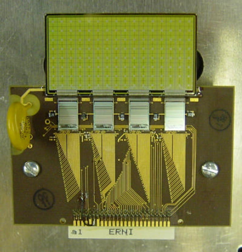
Silicon pad sensor (32×16 array of 1.4 mm square pad and 1 mm thickness) manufactured by SINTEF and four VATAGP3 128-channel readout chips.
The four VATAGP3 ASIC chips developed by IDEAS for the readout system are mounted and wire-bonded along one side of the silicon sensor. They are shown at the center of the photograph in Fig. 1. The VATAGP3 contains 128 charge sensitive amplifiers and slow shapers for VA part with sample-and-hold and a multiplexer for sequential readout. The VATAGP3 also contains 128 fast shapers for the TA part followed by discriminators. This allows the use of this chip in a self-triggering configuration and the possibility of three readout modes: serial, sparse, and sparse with adjacent channels. A block diagram of the VATAGP3 is shown in Fig. 2. In the slow analog chain, a sample and hold signal is applied at the peaking of the slow shaper signal (3 μs) in order to store the peak value to be readout later. In the fast chain, the signal from the fast shaper (approximately 200 ns peaking time) is applied to a discriminator, and the outputs of all the 128 discriminators are ORed together and provide the trigger for the data acquisition. Each discriminator output is also stored in a register. If the sparse readout mode is used, only the analog values of the channels for which the discriminators were above threshold will be read, together with the channel address. Each discriminator output can be masked. The discriminator threshold can be adjusted for all channels in common. Moreover, threshold offsets can be adjusted individually for each channel using a 3-bit DAC. Other features are the possibility of increasing the gain of the fast shaper in 4 steps (2 bits) and the injection of a calibration pulse into each channel. This last feature is very useful to test the electronics in the absence of the sensor.
Fig. 2.
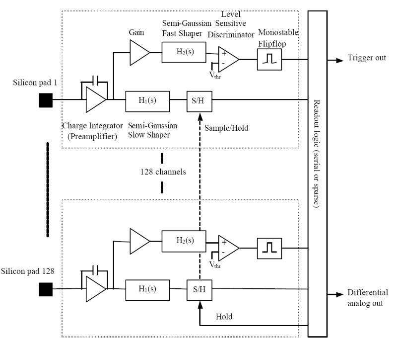
Block diagram of VATAGP3 readout chip.
3. Silicon detector performance
The baseline offset (pedestal) is associated with each individual silicon pad. Since each pad uses a different preamplifier/amplifier pair, some variation in baseline is expected. The offsets also vary slightly with time and temperature. In order to reference all pads to a common zero voltage level and eventually achieve the best possible energy resolution, the pedestal must be subtracted from the measured signal. Common-mode noise is a positively correlated noise component among all pads. This may result from bias voltage fluctuations, ground plane shifts, and other sources that affect all pads simultaneously. Common mode noise determination is made for each detected event. As the pedestal, this correction is commonly completed during post-processing with the raw data from all pads. A probe containing a 99mTc source (140 keV photons) was mounted inside a lead collimator placed several centimeters above the silicon sensors, uniformly illuminating all pads. The discriminator threshold was set at 30 keV—as low as possible while still above the noise level.
Since for each event most of the pads will have no signal except for one or two pads with radiation interaction, values read from each pad except those pads having true event are used to estimate pedestals and common mode noise. Common mode noise is calculated by averaging ADC values of the appropriate pads after subtracting the corresponding pedestal; this noise estimate is subsequently subtracted from the pads where radiation interactions occurred.
Pedestals and noise (standard deviations of the pedestals) of all 512 pads of one of the silicon sensors are illustrated in Fig. 3. Average pedestal values of all channels in the first and second silicon detectors are 153.2 ± 2.32 and 126.8 ± 2.22 ADC, respectively. Two noisy channels 224 and 225 in the first silicon detector are masked. Fig. 4 shows the distribution of common mode noise for the two silicon detectors. Distributions are Gaussian-shaped with zero mean and 1.53 and 1.55 ADC FWHM from the first and second detectors, respectively.
Fig. 3.
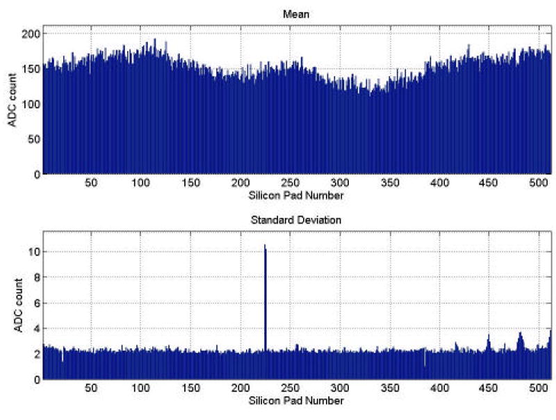
Mean values (top) and standard deviations (bottom) of pedestals in ADC counts measured from the first silicon sensor.
Fig. 4.
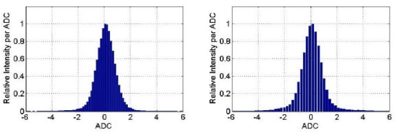
Histograms of common mode noise from the first (left) and second (right) silicon detectors. The distributions are Gaussian-shaped with zero mean and 1.53 and 1.55 ADC FWHM from the first and second silicon detectors, respectively.
The pad-to-pad gain of each silicon sensor was determined by analyzing a 99mTc energy spectrum after correcting for the baseline offset and common mode noise. If the signal amplitudes in a pad exceeded its threshold, the signal amplitudes of all 512 pads were sampled at their maximum, read out, and digitized sequentially.
Fig. 5 show the pad-to-pad gain and resolution variation from a Gaussian fit to the measured peak ADC channel data for each individual pad in the first silicon detector. The double calibration point for each pad was used to convert ADC channel into energy. One calibration point is at 140.5 keV peak from 99mTc and the other is at 74.969 keV peak from lead Kα1 X-ray. The measured uniformity of the pad gain is excellent, showing less than 7 % variation. Energy resolution from all pads is also uniformly distributed in the two silicon detectors. Channels 21 and 384 in the first and channel 191 in the second silicon detector were masked off due to abnormal gain and energy resolution.
Fig. 5.
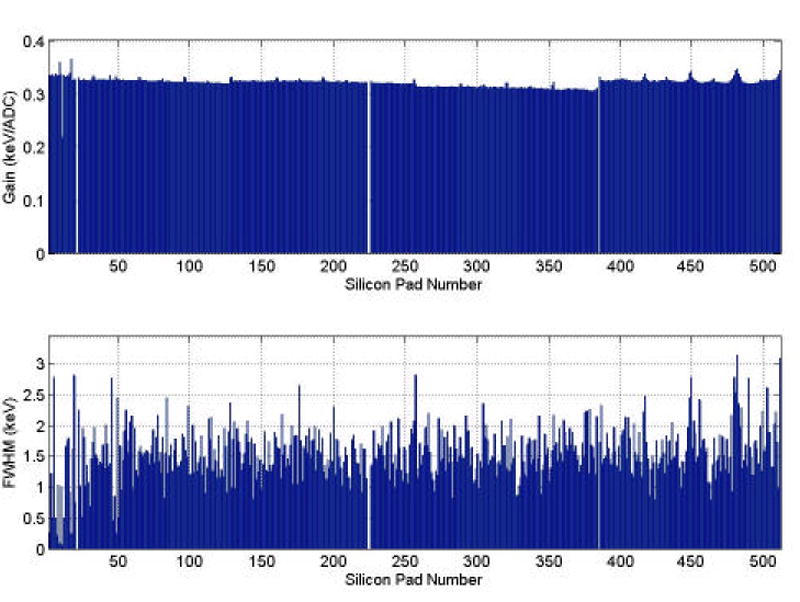
Gains (top) and pad-to-pad energy resolutions (bottom) from all channels of the first silicon sensor using 99mTc source.
Since the silicon detector has 512 independent silicon pads, 512 energy calibration curves are required. Gain corrected energy spectra for 241Am and 99mTc sources are shown in Fig. 6 from the second silicon sensor. These spectra were acquired with a relatively low TA LLD setting of 35 keV, but higher than minimum threshold (25 keV). The photopeak region in each spectrum was fitted by a Gaussian function to estimate energy resolution. Fitted resolutions at the 59.5 keV photopeak energy of 241Am were 1.49 and 1.45 keV FWHM for the first and second sensors. Corresponding values at 140.5 keV were 1.39 and 1.38 keV FWHM. The Compton continuum for the 99mTc photons is clearly visible in both acquired spectra. It starts from discriminator threshold and extends to the Compton edge at 49.8 keV. In addition to expected features, the 99mTc spectra show several lead X-rays peaks (Kα1, Kα2, Kβ1, Kβ2, and Kβ3) that occur because the source was contained inside a lead collimator. X-ray peaks from 84.936 keV Kβ1 and 84.450 keV Kβ3 cannot be separated since the energy difference between two X-rays is 0.486 keV—about three times smaller than detector energy resolution. The measured energy and relative intensities of from these X-rays peaks are in excellent agreement with values from literature as listed in Table 1 [17].
Fig. 6.
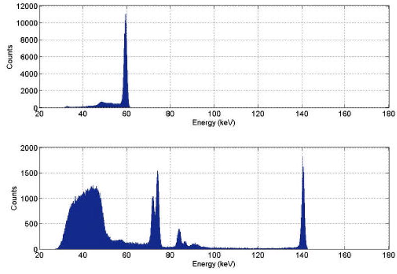
Energy spectrum after gain correction from all 512 pads of the second silicon sensor with 241Am (top) and 99mTc (bottom). Energy resolutions are 1.45 keV FWHM at 59.5 keV of 241Am photopeak and 1.38 keV FWHM at 140.5 keV of 99mTc photopeak.
Table 1.
207Pb K-shell X-rays
| 207Pb K-shell X-ray | Energy (keV) | Intensity* |
|---|---|---|
| Kα1 | 74.969 | 100 |
| Kα2 | 72.804 | 59.3 |
| Kβ1 | 84.936 | 22.2 |
| Kβ2 | 87.300 | 10.2 |
| Kβ3 | 84.450 | 11.6 |
Intensities are normalized to 100 for the Ka1 line.
4. Prototype PET system
In order to achieve the sub-millimeter spatial resolution performance, the prototype setup for a small animal PET using high resolution silicon pad detectors was constructed. The first prototype setup for 3-D PET scanner consisting of 1 mm thickness and 22.4 mm axial FOV and 44.8 mm transaxial FOV was built by placing two silicon pads arrays facing each other. The first experimental setup has low sensitivity problem due to the thin silicon thickness. To provide high enough sensitivity without DOI loss, multiple-thin-layer detectors were required. Detector arrangement using multiple-layer detector modules are described in section 7. Since the silicon detectors used in the first setup were only 1 mm thick, the only way to have sufficient thickness with two thin detectors is to position the two detectors edgewise on opposite sides of the source to generate slice or cross sectional image with reasonable sensitivity. Fig. 7 shows the prototype setup of the PET for a single slice instrument. The experimental setup is composed of two silicon pad detectors, a source turntable, tungsten slit collimator and lead shielding. Electronics include a NIM coincidence unit and silicon detector readout systems. The silicon detectors were located edgewise on opposite sides of a 5 cm FOV to maximize efficiency. Geometric alignment of silicon detectors was performed using a laser line-source as illustrated in Fig. 7 and detailed below. Fig. 8 shows cross-sectional view of the experimental setup.
Fig. 7.
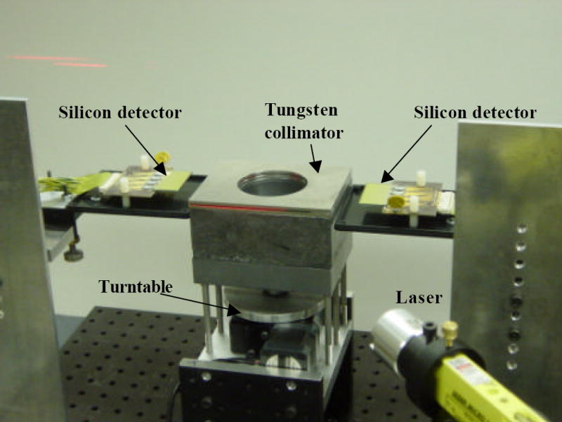
Photograph of the prototype PET consisting of two silicon pad detectors, a source turntable, lead shielding and tungsten collimator.
Fig. 8.
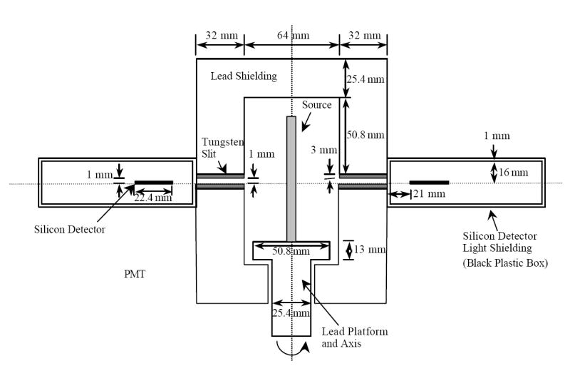
Cross-sectional view of the prototype setup.
For mechanical protection, each silicon detector was mounted in a black plastic box fixed on the platform. The platform has three leveling screws and is fastened to a 3-D position adjustable stand controlled by micrometers on an optical alignment breadboard to allow precise positioning. Geometric alignment is performed by tilting and adjusting platform position while illuminating the edge of silicon detector through the 1 mm wide tungsten slit with a horizontal laser beam because overall detection efficiency is extremely sensitive to geometric alignment. The active FOV was shielded with a lead block and collimated with two 3 mm thick tungsten slabs with a 1 mm gap.
A block diagram of the coincidence and data acquisition electronics is shown in Fig. 9 for the PET system. Timing pulses from the silicon detector are generated from the TA section in VATAGP3. The common trigger for each detector (an OR of all 512 channels) passes through a timing alignment unit consisting of gate and delay generator. The width of the silicon trigger signal is adjusted for coincidence timing window. The silicon triggers are input to a coincidence unit (EG&G-ESN CO4010, quad 4-fold logic unit). If the event occurs within a preset coincidence window a logic pulse is generated that leads to full event readout from VME-DAQ ADC. The VME based readout unit processes and “sparsifies” the raw data such that energy from each silicon pad are buffered and eventually transferred to a PC in the list mode as shown in Fig. 9.
Fig. 9.
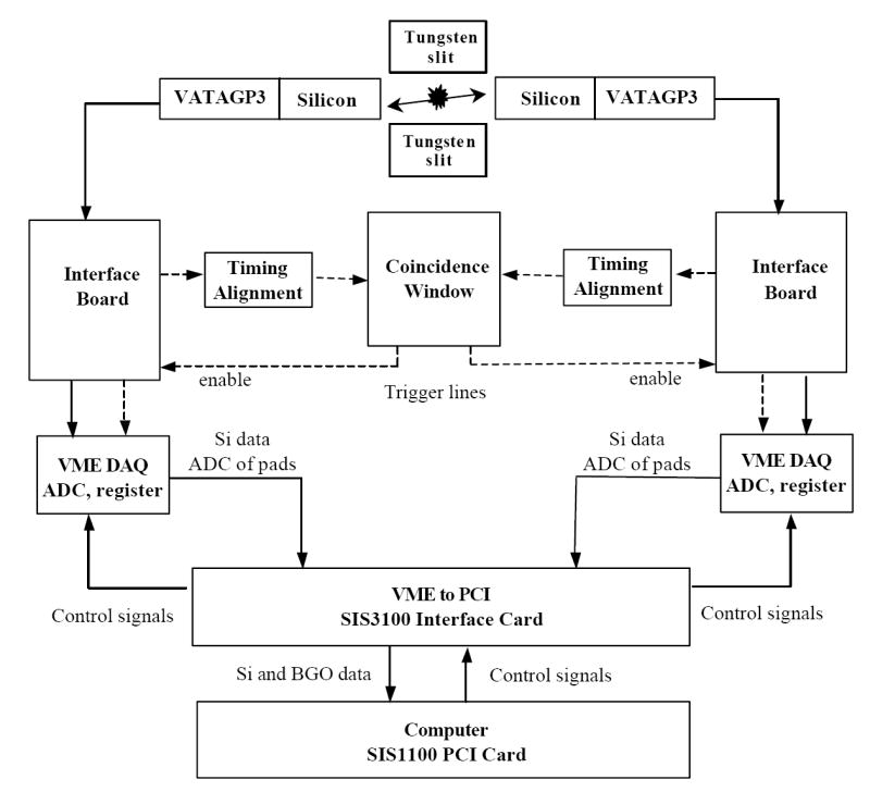
Block diagram of the prototype system.
5. PET performance
Timing measurements were conducted between two opposed silicon detectors using 511 keV annihilation photons from an 18F source located at the center of the FOV. Silicon TA trigger signals from of the VATAGP3 were fed to an ORTEC 566 time-to-amplitude converter (TAC). Both silicon detectors accepted all events above a TA LLD threshold of 30 keV.
Fig. 10 is the measured timing curve from trigger signals using only two silicon detectors and shows a timing resolution of 82.1 ns FWHM. The poor timing resolution of the silicon detector is a result of the wide energy range of detected Compton recoil electrons (30-340 keV) coupled with the simple leading-edge threshold trigger of present VATAGP3 chips. This is also referred to as “amplitude walk.” Due to the amplitude walk, a wide coincidence timing window (200 ns) is necessary in order to maintain adequate efficiency for true coincidence events.
Fig. 10.
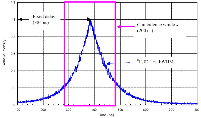
Coincidence timing spectrum from two silicon detectors of the prototype setup using 18F source. Timing resolution is 82.1 ns FWHM.
As we discussed before, geometric detector alignment is very important to maximize detection efficiency. After alignment was performed (Fig. 7), the coincidence efficiency with two silicon detectors were measured using an 18F point source. A 1.1mm I.D. glass capillary tube was loaded with 480 μCi of 18F-FDG and located of the center of the FOV. The height of source in the capillary tube is 2.5 cm. The portion of source activity in 1 mm gap tungsten slit is 19.2 μCi. The edge-to-edge distance between two silicon detectors is 17 cm. Detectors were operated only at 100V bias for protection while they deplete at ~180V. The TA LLD setting is 35 keV on both silicon detectors. The number of ORed silicon TA trigger signals from the VATAGP3 chips was counted using an ORTEC 994 CCNIM dual counter and timer. The trigger rate was measured independently from data acquisition. Since data acquisition from all pads requires appreciable processing time, the number of triggers is different depending on the amount of data stored.
From the experiment to measure coincidence efficiency using a 200 ns coincidence timing window, coincidence counting rates were measured at 7.4 ± 0.8 cps. Overall coincidence detection efficiency is calculated as 1.04 × 10⁻³ %.
Coincidence data were acquired using two silicon detectors with a 200 ns coincidence timing window. The TA LLD was set at 35 keV on both silicon detectors. A plastic tube with 4 mm inner diameter contained 18F. The source was approximately located at the center of FOV (after analyzing the data, we found that the source is located at 3-4 millimeters below the center of FOV). Serial mode acquisition was used for silicon data readout. After pedestal, common-noise, and gain corrections in data post-processing, the events having multiple signals in all channels caused from multiple scatters or multiple events in coincidence window were rejected to reduce position ambiguity. However, some of multiple scatter events, if energy is fully deposited, can be used for position estimation using Compton kinematics [18-19].
Fig. 11 shows 2-D plot of the number of coincidence events in each pad or hit map from both detectors. Since there is no opposing detector element for the off-axis source, the pads on the top of both silicon detectors shouldn’t have coincidences. However, a few counts (1-3) were measured in these channels. These are likely due to random coincidences. The 2-D hit map shows no events in channels that were masked (channel 21, 224, 225, and 384 in the first silicon detector and channel 191 in the second silicon detector) which before in the pedestal and gain calculations. A 3-D plot of the number of coincidence events in the each pad or hit map from the detectors are shown in Fig. 12. The 3-D hit map shows that the number of interactions is exponentially decreasing with silicon detector thickness due to photon attenuation. Fig. 13 illustrates LOR plot from 1000 coincidence events using two silicon detectors. Finally, we can verify that the source is located at 3-4 millimeters below the center of FOV and the counts measured in the pads which have zero coincidence detection probability are result from random coincidence events with Fig. 13.
Fig. 11.
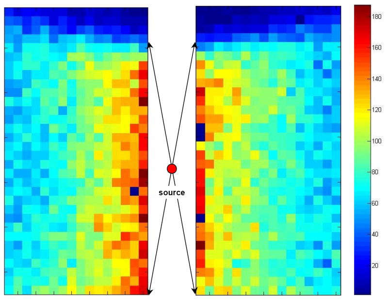
2-D plot of the number of coincidence events in each pad or hit map from the first (right) and second (left) silicon detectors. The source is located at few millimeters below from the center of FOV.
Fig. 12.
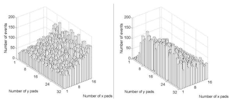
3-D plot of the number of coincidence events in each pad or hit map from the first (right) and second (left) silicon detectors.
Fig. 13.
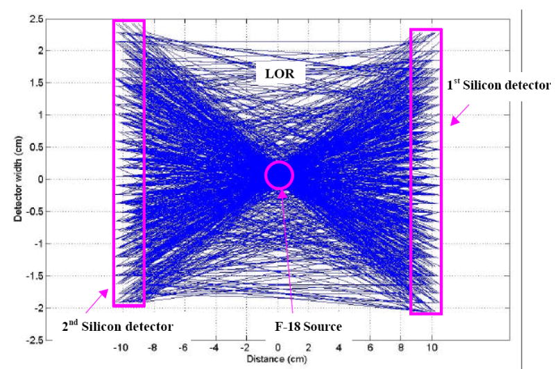
LOR plot from 1000 coincidence events using the first (right) and second (left) silicon detectors.
6. Reconstructed images
Image data were acquired to characterize the spatial resolutions of the imaging systems using the two 18F line sources. The sources and the tomographic setup are shown in Fig. 8. FDG was filled in each 1.1-1.2 mm inner diameter glass capillary tube with 0.2 mm thick wall. The effective source activity which is the portion of source activity in the 1 mm gap tungsten slit was 17 μCi. An empty glass capillary tube was placed between two sources. Two sources were separated by 2 mm edge-to edge and 3 mm center-to-center. In order to acquire a dataset with complete angular sampling, the angular step size of the rotation was set to 15 degrees. The LOR data drawn with hit positions in both silicon detectors from the 42,524 coincidence events (54 % of the total events) were placed into a 128 by 200 distance-angle sinogram. Each bin size was 0.4 mm by 0.9 degree. Hit position was randomly selected in the interaction pad to increase linear and angular sampling without using a PET wobble motion.
Image in Fig. 14 was reconstructed using conventional 2-D FBP with a ramp filter having a cutoff at the Nyquist frequency. Sensitivity distribution in the FOV, scatter, and random events were not corrected in the reconstruction. Fig. 14 shows that the systems clearly resolve the two line sources. The center-to-center distance of two line sources on the image is 3 mm in agreement with the measured distance. The image resolutions of the PET are 1.45 mm and 1.47 mm FWHM obtained from 1-D profiles of two line sources using Gaussian fit.
Fig. 14.
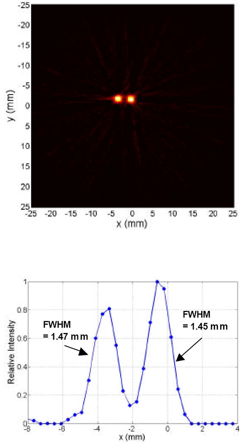
Two line source image from 18F-FDG in two glass capillary tubes (1.1-1.2 mm I.D.). The gap between two sources is 2.0 mm. 2-D FBP with a ramp filter having a cutoff at the Nyquist frequency was used to reconstruct image. (Top): 2-D image. (Bottom): 1-D profile of the 2-D image.
In order to achieve the best spatial resolution of the scanner, interaction position was estimated without ambiguity by rejecting multiple events with the high energy resolution (< 1 %) and small silicon pixel size (1.4 mm2). The multiple events (46 % of the total events) also have been included in spatial resolution calculation with the first interaction estimation schemes, including maximum signal pixel, the second maximum signal pixel, the centroid of signal distribution, and the signal-producing pixel nearest the source, proposed by Shao and Cherry [20], Comanor and Moses [21], and Miyaoka and Lewellen [22]. The tails of the distribution caused degradation in image contrast and noise in the image, rather than a loss in image resolution. The effect of multiple events on spatial resolution was negligible. The spatial resolution (FWHM) of the detectors is dominated by the pixel size and positron physics, and not scatter in the detector or between the detector layers. This result has been already proved by Stickel [3], Shao and Cherry [20].
The resolution uniformity across the FOV of the prototype setup was evaluated using a multiple line source. The source, 18F-FDG in glass capillary tubes, consists of five line sources located at center of the FOV and r = 2, 5, 10, and 20 mm from the center. The effective activity of each source was intended to be identical and was about 21 μCi. The source was rotated with 10 degree steps.
From the reconstructed five line source image using 2-D FBP in Fig. 15, image resolutions (both radial and tangential resolution) are uniformly distributed across the FOV between 1.2–1.7 mm FWHM. Since the DOI was measured from the 1.4 mm pixels in 16 layers of the silicon detectors, nearly uniform resolution in the FOV was obtained.
Fig. 15.
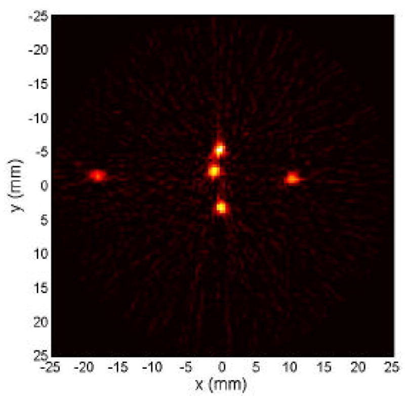
Five line source image reconstructed with 2-D FBP with ramp filter. The source (18F-FDG in glass capillary tubes) located at r = 0, 2, 5, 10, and 20 mm from the FOV.
The 18F extended source that was imaged was a multiple line source in the shape of an “M”. To make the line source, 18F activity of approximately 5.0 μCi/mm3 was injected into each glass capillary tube. Two vertical lines were 20 mm long and separated by 20 mm. Two lines in the middle were 15 mm long. The source was rotated 180 degrees in 5 degree steps.
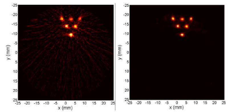
The images and contours in Fig. 16 were reconstructed using a ML-EM method without regularization at iteration 30. The geometric system matrix obtained from forward and backprojection was used in the ML-EM method. The detector sensitivity, scatter, and random events were not corrected in the image reconstruction. The ‘M’ shape is immediately apparent, although the vertical line on the right is barely visible since the line source was mistakenly positioned out of the measurement volume of the tomograph. The 20 mm vertical separation of the two vertical lines is very well resolved by the 2-D and contour images.
Fig. 16.
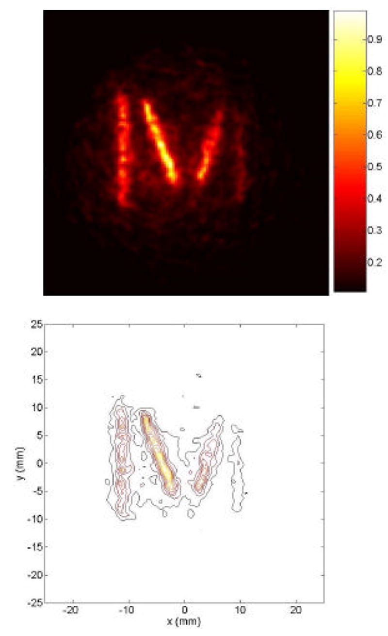
2-D (top) and contour (bottom) images reconstructed with a ML-EM (30 iterations) using four 18F line sources in “M” shape. The size of each image is 5 cm × 5 cm.
In order to include scatters in object, image data from six line sources in a scatter medium were acquired. 18F-FDG was filled in 1.1 mm diameter hot rods of a resolution phantom (a Lucite cylinder with a 4.4 cm diameter and 3.4 cm height). Center-to-center spacing of hot rods is 5 mm. The effective activity of each source was about 21 μCi.
Images in Fig. 17 were reconstructed with 2-D FBP with ramp filter and ML-EM with 20 iterations. Attenuation, scatter, and random events were not corrected in the both images. The 5 mm spacing is resolved easily in the both images. The measured image resolutions of the line sources at different positions in the FOV were consistent with earlier values from 2-D FBP. The typical streak artifacts in FBP image were remarkably reduced using the ML-EM algorithm.
Fig. 17.
Six line source images reconstructed with 2-D FBP (left) with a ramp filter having a cutoff at the Nyquist frequency and 2-D ML-EM (right) with 20 iterations. Attenuation, scatter, and random were not corrected in the both images. 18F-FDG was filled in 1.1 mm diameter hot rods of resolution phantom (a Lucite cylinder with a 4.4 cm diameter and 3.4 cm height). Center-to-center spacing of hot rods is 5 mm.
7. Summary and discussions
The ultimate goal of this work is to develop a very high resolution small animal PET instrument that can achieve sub-millimeter spatial resolution. We constructed a prototype PET instrument consisting of two silicon pad detectors (32 × 16 array of 1.4 mm square pad and 1 mm thickness).
The resolution of the theoretical predicted value is 0.7 mm FWHM which is half of the 1.4 mm silicon pad width. However, the image resolution of the prototype is measured to be 1.45 mm FWHM. This prediction is based on several assumptions with the resolution blurring factors. First, the blurring from the positron range is very small due to using 18F which emits a lower energy positron than other isotopes such as 11C, 13N, and 15O. Second, the blurring function from annihilation photon acolinearity is negligibly small if the system diameter is small. Third, the response function from detector width is only a blurring source. Finally, the source size is an impulse function.
Since the size of the line source diameter is 1.1–1.2 mm, it can not be neglected and must be considered to calculate intrinsic system resolution by de-convolving source size from the image resolution. Alternatively, if one could make a very small source, image resolution would be very close to intrinsic resolution. In addition, the acolinearity contribution (0.374 mm FWHM in Gaussian distribution) due to about 170 mm system diameter is not negligible. These resolution blurring factors were convolved with the 0.7 mm FWHM triangular response and then reconstructed. For this reason, intrinsic PET resolution was estimated to be about 600-800 μm FWHM with the de-convolution of the source size and acolinearity from the image.
There are a number of challenges presented by the design and construction of an actual complete system depending on the imaging applications. These include silicon pixel size, production cost, dense detector packaging and cooling, and timing performance.
The highest spatial resolution was limited primarily by the silicon detector pixel size. For example, reducing the detector element size from 1.4 mm to 0.3 mm square improves resolution from 700 μm to 340 μm FWHM. Nevertheless, small pixels sizes equate with higher costs due primarily to a larger number of electronic channels. In any case, a practical limit to the spatial resolution results from possible migration of the recoil electron between detector pixels and the range of the positron before annihilation in the object. In order to determine the minimum silicon pixel size, further studies are required including additional recoil electron transport simulations in silicon.
Ideally, for PET, timing resolution would be less than 10 ns FWHM. Timing window of conventional PET scanners is between 2 and 10 ns. Due to the large timing uncertainty of the silicon detector (82.1 ns FWHM timing resolution), a wide coincidence timing window (200 ns) is necessary in order to maintain adequate efficiency for true coincidence events. Besides true events, there are scatter and attenuation in the object which lead to a high singles to coincidence fraction. These taken together with the wide coincidence timing window will lead to high random coincidence rate in the scanner. In order to overcome the drawback, it is obvious that we need to develop new silicon detector trigger system. The poor timing resolution of the silicon detector is a result of the amplitude walk. Therefore, the amplitude walk correction methods using constant fraction discriminator or correcting timing signal as a function of the recorded pulse-height for each event should greatly improve timing performance (~5-10 ns FWHM) [23] even with the current detector and readout ASICs.
The prototype setup has very low coincidence efficiency 1.04 × 10⁻³ % because of using only two small area silicon detectors. Dense detector packaging is required to improve detection efficiency but at increased cost and cooling. Fig. 18 shows a stack of silicon module and two detector arrangements for a multi-slice PET scanner design in order to image reasonable size metabolic regions in small animals. The module consists of five detectors placing on top of each other as shown in Fig. 18. For examples, a scanner having 44.8 mm transaxial FOV constructed with four silicon detector modules will require a total of 10240 readout channels (512 channels/detector × 5 detectors/module × 4 modules). To reduce the number of readout channels from M×N to M+N, silicon pad detectors can be replaced with double-side silicon strip detectors. If we assume no gap in the multiple-layer module, one system (edgewise arrangement) has 5 mm axial FOV with 22.4 mm thickness and the other (surface facing arrangement) has 22.4 mm axial FOV and 5 mm thickness. As axial FOV increases from 5 mm to 22.4 mm, geometric efficiency (the solid angle subtended by detector modules) increases from 11.1 % and 44.7 %. Decreasing silicon detector thickness from 22.4 mm to 5 mm, intrinsic detection efficiency for singles decreases from 36.1 % to 9.5 %. In reality, packing fraction and coincidence efficiency of the arrangements will decrease due to the gaps (~1-2 mm) between the layers in the detector module.
Fig. 18.
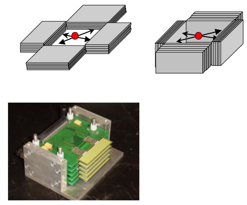
(Bottom): A stack of silicon module. (Top): Detector arrangements used in a multi-slice PET scanner design using four silicon modules.
Continuing efforts are expected to investigate these challenges and will support the conclusion that a very high resolution small animal PET based on multiple-layer silicon detector modules can achieve sub-millimeter resolution with high efficiency and good timing resolution.
Acknowledgments
This work is supported by the United States National Institute of Health under Grant EB000430-31 and RR15133.
Footnotes
Publisher's Disclaimer: This is a PDF file of an unedited manuscript that has been accepted for publication. As a service to our customers we are providing this early version of the manuscript. The manuscript will undergo copyediting, typesetting, and review of the resulting proof before it is published in its final citable form. Please note that during the production process errors may be discovered which could affect the content, and all legal disclaimers that apply to the journal pertain.
References
- 1.Yang Y, et al. Phys Med Biol. 2004;49:2527. doi: 10.1088/0031-9155/49/12/005. [DOI] [PubMed] [Google Scholar]
- 2.Tai Y, et al. Phys Med Biol. 2003;48:1519. doi: 10.1088/0031-9155/48/11/303. [DOI] [PubMed] [Google Scholar]
- 3.Stickel JR, Cherry SR. Phys Med Biol. 2005;50:179. doi: 10.1088/0031-9155/50/2/001. [DOI] [PubMed] [Google Scholar]
- 4.Clinthorne NH, et al. J Nucl Med Suppl. 2000;41:20. [Google Scholar]
- 5.Park S, et al. J Nucl Med Suppl. 2001;42:55. [Google Scholar]
- 6.Park S, et al. IEEE Nucl Sci Symp Conf Record. 2001;2:1120. [Google Scholar]
- 7.Park S, et al. IEEE Nucl Sci Symp Conf Record. 2002;3:1756. [Google Scholar]
- 8.Park S, et al. IEEE Nucl Sci Symp Conf Record. 2004;6:3911. [Google Scholar]
- 9.Tai Y, et al. J Nucl Med. 2005;46:455. [PubMed] [Google Scholar]
- 10.Weilhammer P, et al. Nucl Instr and Meth. 1996;383:89. [Google Scholar]
- 11.Meier D, et al. IEEE Trans Nucl Sci. 2002;49:812. [Google Scholar]
- 12.Studen A, et al. Nucl Instr and Math A. 2003;501:273. [Google Scholar]
- 13.Studen A, et al. Nucl Instr and Math A. 2004;531:258. [Google Scholar]
- 14.The Computer Imaging for Medical Applications (CIMA) collaboration. http://www.cima-collaboration.org.
- 15.Integrated Detector and Electronics (Ideas ASA) http://www.ideas.no.
- 16.SINTEF, Foundation of Scientific and Industrial Research at the Norwegian Institute of Technology, Electronics and Cybernetics, Microsystems. Oslo and Trondheim; Norway: http://www.oslo.sintef.no/ecy/ [Google Scholar]
- 17.L’Annuziata Michael F. Handbook of Radioactivity Analysis. Academic Press; San Diego, USA: 1998. [Google Scholar]
- 18.Kamae T, Enomoto R. U.S Patent 4,857,737. 1989
- 19.Kroeger RA, et al. IEEE Trans Nucl Sci. 2002;49:1887. [Google Scholar]
- 20.Shao Y, et al. IEEE Trans Nucl Sci. 1996;43:1938. [Google Scholar]
- 21.Comanor KA, et al. IEEE Trans Nucl Sci. 1996;43:2213. [Google Scholar]
- 22.Miyaoka RS, Lewellen TK. IEEE Trans Nucl Sci. 2000;47:1614. doi: 10.1109/TNS.2007.905164. [DOI] [PMC free article] [PubMed] [Google Scholar]
- 23.Mikuz M, et al. IEEE Trans Nucl Sci. 2002;49:2549. [Google Scholar]