

Abstract
Electrically conductive polymers, such as polypyrrole (PPy), show promise for modifying the dimensions and properties of micro- and nanoscale structures. Mechanisms for controlling the formation of PPy films of nanoscale thickness were evaluated by electrochemically synthesizing and examining PPy films on planar gold electrodes under a variety of growth conditions. Tunable PPy coatings were then deposited by electropolymerization on the sidewalls of individual, electrically addressable carbon nanofibers (CNFs). The ability to modify the physical size of specific nanofibers in controllable fashion is demonstrated. The biocompatibility, potential for chemical functionalization, and ability to effect volume changes of this nanocomposite can lead to advanced functionality, such as specific, nanoscale valving of materials and morphological control at the nanoscale.
Keywords: Carbon nanofibers, Polypyrrole, Electropolymerization, Surface modification, Nanomaterial
Introduction
The physical and electronic properties of conjugated polymers allow for a variety of applications. Their semiconducting properties enable their use as thin film transistors [1-4], light-emitting diodes [5,6], and novel analytical sensors [7,8]. In some cases, conjugated polymers can also change volume in response to electrical signals, providing a means for creating microactuators [9,10]. One of the better-studied conducting polymers is polypyrrole (PPy). Its popularity can be attributed to its high chemical stability, ease of preparation, and commercial availability. Polypyrrole is a conducting polymer whose polymerization is initiated by monomer oxidization using chemical or electrochemical techniques [10,11]. High quality films can be synthesized by the electrochemical methods first reported by Kanazawa et al. in 1979 [12]. Although significant attention has focused on microscale patterning and growth of conducting polymers, such as PPy, for various electronic applications, relatively little attention has focused on electropolymerization as a means for morphologically modifying micro- or nano-scale physical structures with thin films of polymer.
Commonly used techniques for creating thin films include the Langmuir-Blodgett method, vapor deposition, sputtering, and spin-coating [13,14]. Precise layering of a variety of materials can be accomplished to create micro- and nano- scale structures across wafer-scale dimensions. Such techniques are routinely used for creating microelectrical mechanical systems (MEMS) and microelectronic systems. However, these processes can require high temperatures, extremely low pressures, or organic solvents. Such conditions make integration of these techniques with biomolecular systems problematic. In contrast, PPy films can be electrochemically deposited at room temperature and under aqueous conditions. Typically, this is accomplished by anodic oxidation of the pyrrole monomer in an ionic solution, an environment compatible with biomolecules. A number of biochemical immobilization methods exploit pyrrole polymerization [15,16]. To initiate polymerization, an electrically active scaffolding material is required and serves as a backbone for formation of the PPy film. This can enable an alternate approach to selective patterning of thin films. That is, addressable electrodes can be used in place of the photolithography-dependent techniques that are required in conventional patterning processes. The thickness of the resulting polymer film can be tailored by controlling the amount of electric charge that passes through the circuit during electropolymerization [17]. The controllability, addressability, and biocompatibility of pyrrole films can be significant advantages when complex fabrication schemes or the synthesis of tunable nanocomposite materials are required.
Here we investigate the use of PPy films for controllably modifying vertically aligned carbon nanofibers (CNFs) with high spatial precision. CNFs can be deterministically grown, allowing for command of their length, shape, orientation, and chemical composition [18-20]. CNFs are nanoscale materials, with diameters on the order of 100 nm, or less, and with lengths up to several tens of microns [21]. Patterned catalyst particles determine the placement of individual fibers or forests of CNFs, which are grown by a plasma enhanced chemical vapor deposition (PECVD) process. CNFs are compatible with a variety of MEMs-based processing techniques, can be conjugated with biomolecules, and are electrically addressable [22-25]. This combination of features enables the incorporation of nanoscale elements within larger (wafer) scale structures, thereby enabling a wide range of applications, including electron emission devices, gene delivery structures, and synthetic membranes [25-28].
Carbon nanofibers can be used as microelectrodes, as demonstrated in such applications as electrochemical probes [23] and sensors [24]. The ability to electrically address individual carbon nanofibers also presents a route to selectively controlling their shape through electropolymerization. Examples of carbon nanotube (CNT) surface modification by polymerization of polypyrrole exist in the literature. In these studies, thin polypyrrole coatings (10 nm – 93 nm) are used to modify the electrical properties or surface chemistry of bulk addressed, stochastically grown forests of CNTs [29,30]. This suggests the possibility of depositing polypyrrole films on individually addressable carbon nanofiber electrodes as a means of selectively modifying their geometry and other properties.
CNF arrays are promising, three-dimensional scaffolds for the synthesis of PPy nanocomposites. A tunable PPy film on the surface of arrays of carbon nanofibers would be useful for integration with MEMs and biomimetic devices. Specific to current interests, a greater understanding of this nanocomposite would be essential for designing membrane structures with defined pore sizes. Previous efforts have demonstrated the utility of CNFs to create membranes within microfluidic structures [27,28,31]. In this application, the physical spacing between nanofibers determines the pore size. CNF growth typically leads to average pore spacings on the order of 300 nm. Reducing the spacing by increasing the diameter of the CNFs can lead to molecular-scale sieving. The electropolymerization of PPy is an attractive route to realizing this goal. Further, the biocompatibility, potential for chemical functionalization, and ability to effect volume changes in PPy can lead to advanced designs that allow for the specific gating of materials. Here we demonstrate that electropolymerization of PPy can modify the physical size of specific nanofibers in a controllable fashion.
Experimental
Materials
Pyrrole monomer was obtained from Acros Organics. Silicon wafers with and without 1 μm of thermal oxide were obtained from Silicon Quest International (Santa Clara, CA). Potassium chloride and 1 M sulfuric acid of reagent grade were obtained from Sigma Aldrich.
Wafer Preparation
For PPy film characterization, planar electrodes were prepared on SiO2 wafers. Metal layers were deposited on these wafers using the electron beam evaporation (EBE) technique (50 Å Ti, 2000 Å Au). The wafers were then diced using a DiscoDad – 2H6T wet dicing saw into strips 0.5 cm wide and 4 cm long.
For PPy-CNF nanocomposite characterization, 100 Å Ti, 500 Å W, 100 Å Ti, 50 Å Si metal stacks were deposited on SiO2 wafers using EBE. The wafers were then vapor primed with hexamethyldisilazane (HMDS) priming agent and photoresist was spin coated. Nickel catalyst sites for CNF growth were then defined using UV–optical projection lithography (GCA AutoStep 200). Resulting catalyst sites were 500 nm in diameter and were patterned at a 5 μm pitch. After a post exposure bake and development, residual photoresist was removed in an oxygen plasma. Catalyst metal, 500 Å Ni, was deposited by EBE on the wafers and the excess metal was removed using an acetone liftoff process. CNF growth was then performed using a previously described PECVD process [19-21]. Resulting CNFs were, on average, 10 μm tall and 500 nm thick halfway between the base and the tip (where measurements were made). After growth, an additional layer of photoresist was spin coated on these wafers to pattern leads for addressing the CNFs. The interconnect pattern was defined using a contact aligner. After development, residual photoresist was removed by an oxygen plasma treatment. The metal stack in the exposed areas of the wafer was then etched away using an SF6/O2/CF3 based plasma for 7 minutes. This provided arrays of electrically addressable nanofibers, as well as unaddressed “control” nanofibers in adjacent regions where metal was removed. The wafer was stripped of remaining photoresist with acetone and the defined leads were wire bonded to a custom printed circuit board. A circle of epoxy (FDA2T, Tracon, Bedford, MA) was painted around the perimeter of the device, forming a fluidic well to confine subsequent electrochemical deposition/analysis.
Characterization Tools
The electropolymerization of PPy was controlled using a Model 660A CH Instruments Electrochemical Analyzer. PPy film thicknesses were quantified in solution using the acoustic AC mode of a Molecular Imaging PicoPlus AFM system. Data analysis software was written in Matlab 6.5.0 (Mathworks Inc.). Film roughness and thickness data were obtained from cross– sections through 2D captured, AFM images. PPy-CNF nanocomposites were also investigated using a Hitachi S4700 high-resolution cold cathode field emission scanning electron microscope (SEM).
Polypyrrole Film Growth on Planar Electrodes
Control of the formation of PPy films was investigated by studying the effects of three electropolymerization growth parameters. These were polymerization time, monomer concentration, and applied voltage. Monomer solutions were prepared in 300 mM KCl and 0.01 M H2SO4 and were handled in 1.5 mL centrifuge tubes.
A platinum coil was used as the counter electrode and a Ag/AgCl (3M KCl) electrode with a glass frit membrane was used as the reference. The counter, reference, and gold planar electrode structure were immersed in monomer solution, with care being taken to avoid contact between electrically active surfaces. Constant potential was applied using the electrochemical workstation over a given polymerization time.
For assessing polypyrrole coatings on gold electrodes, an area of polypyrrole in the center of the electrode was typically scraped clean with forceps after polymerization to provide the abrupt change in height necessary for accurate thickness measurements. Polypyrrole film thicknesses were determined from the lateral cross sections of resulting AFM scans, with the gold substrate providing the baseline from which measurements were made.
For variable polymerization time experiments, the monomer concentration was held constant at 20 mM pyrrole. A constant potential of 0.65 V was applied for polymerization times that ranged from 15 s – 180 s. For variable monomer concentration experiments, a constant potential of 0.65 V was applied for 15 s using monomer solutions with concentrations of 10 mM to 500 mM. For variable potential experiments, a 20 mM monomer solution was prepared. Potentials covering a range of 0.7 V – 1.0 V were applied for 15 s.
Polypyrrole Film Growth on Carbon Nanofiber Electrodes
Conditions for polypyrrole film growth on CNF electrodes were based on results from polypyrrole film characterizations on planar gold electrodes. For these experiments, a wire-bonded microelectrode structure was secured in place on top of a metal stand. Pyrrole monomer was prepared at a 20 mM concentration and ∼100 μL was pipetted into a fluidic well formed from epoxy. A single nanofibered lead of the electrode array was connected as the working electrode. The Ag/AgCl reference electrode was positioned above the 100 μL droplet of monomer so that its tip was immersed in monomer but not touching the structure. The platinum counter electrode was similarly positioned from above. A constant potential of 0.75 V was applied for a range of polymerization times from 15 s – 105 s. The structure was then washed in deionized water, dried, and examined in the SEM.
Results and Discussion
For synthesis of PPy films of submicron thickness, we evaluated the effect of polymerization reaction time, monomer concentration, and applied bias on film formation to determine the relative degree of control afforded by these easily manipulated variables. The best variable to use for controlling polymerization was then selected by determining which variable produced a reproducible and linear response in growth rate and quality. Variables such as pH and temperature also have an effect on electropolymerization but, outside of a narrow range, can have deleterious effects on biomolecules and were not considered for controlling film thickness. After evaluating the reaction parameters and selecting the best variable, tunable PPy coatings were deposited on the sidewalls of CNFs.
To facilitate the evaluation of these reaction parameters, PPy films were synthesized on gold planar electrodes. This enabled accurate film thickness measurements using an atomic force microscope. While PPy films nucleate on the surface of gold electrodes differently than on carbon-based electrodes [32,33], the resulting effects are typically limited to physical properties such as surface morphology and crystal structure. In some cases, the electrode material may also have an effect on the polymerization reaction rate. If the electrode does not conduct current uniformly, PPy will nucleate and propagate more quickly on the less resistive areas of the electrode. The formation of oxides on the surface of the electrode can also slow or inhibit the polymerization reaction. Further, some electrode materials are subject to dissolution during electropolymerization. In these cases, anodic polarization leads to dissolution of the electrode material and passivation of the substrate [33]. However, if the electrode material is inert (Au, Pt, glassy carbon) and conducts current uniformly, its participation in the polymerization reaction is negligible [33,34]. Even when the electrode material is subject to dissolution, the effects on the polymerization rate are relatively small [35]. Thus, it is possible to evaluate the effect of reaction parameters on films synthesized on gold and apply these observations as a first order approximation of what will occur with activated carbon-based electrodes.
Studying films in aqueous solution prevents the use of many commonly available characterization instruments, such as conventional electron microscopy tools. The sub-micron features of the sample add further limitations and make tools such as the profilometer less practical. A readily accessible characterization tool was the atomic force microscope (AFM). The AFM is capable of examining samples in aqueous media and is sufficiently sensitive for measuring nanoscale features.
Control of Pyrrole Coating Thickness on Planar Electrodes
Figure 1A demonstrates the relationship between PPy film thickness and polymerization time. To evaluate general film characteristics and reproducibility, AFM measurements were made in aqueous solution (300 mM KCl, 10 mM H2SO4) in three separate areas of each film and on multiple samples (n = 2-4). Polymerization time was found to significantly affect the resulting polymer film thickness. Initially, the polymer film appeared to form relatively slowly before the growth rate stabilized and became linear with time. This initial “lag” may be attributed to heterogeneous electron transfer rates on the electrode surface that may result from surface passivation due to absorbed species or oxidation. Either of these phenomena would reduce the number of nucleation sites for PPy film formation, leading to slow initial film growth until the PPy film coated the entire electrode surface. After the initial “lag, film thickness increased linearly at a rate of 2.6 nm/s. Film thickness was found to vary within each sample by 7% of the total thickness. Measurements between multiple samples showed a variance of 8%, closely matching the intra-sample variance. A correlation between film thickness variance and polymerization time over the range of values investigated was not observed.
Figure 1.
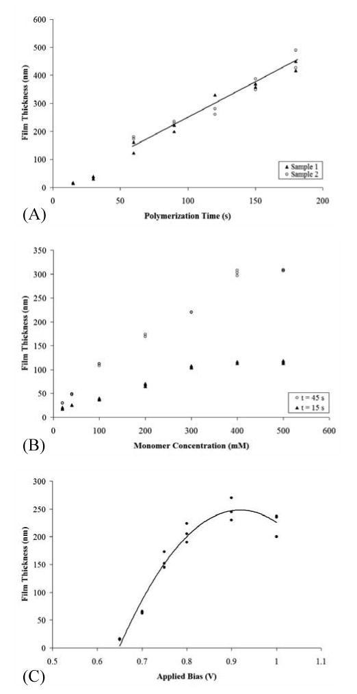
Planar PPy film thickness versus A) polymerization time, B) monomer concentration, and C) applied bias. Data points in A) represent measurements from two separate PPy films, sample 1 (○) and sample 2 (▲). Data points in B) were from samples polymerized for 45 s (○) and 15 s (▲). A second order polynomial trend line was fitted to the data in C).
Variations in the monomer concentration also affected film thickness. For these experiments, polymerization times of 15 s and 45 s were used. Figure 1B displays resulting PPy film thicknesses plotted as a function of monomer concentration. The figure shows a linear dependence at low monomer concentrations and a leveling off at higher monomer concentrations. Within the linear region, increases in film thickness with monomer concentration for the 15 s reactions were on the order of 3 Å/mM monomer. Increases in film thickness for the 45 s reactions were found to be 7 Å/mM monomer. As polymerization time is increased, the changes in monomer concentration have a more pronounced effect on PPy film thickness. The leveling off of the growth rate at higher monomer concentration is likely due to the limited solubility of the monomer in the aqueous phase. Indicated pyrrole concentrations are based on assumed complete solubilization of monomer in the aqueous phase, but values tested approach the estimated solubility limit of 4.5 g/100 g water [36]. Incomplete solubilization would reduce the effective concentration at the submersed electrode.
Figure 1C shows resulting PPy film thicknesses over a range of applied voltages at a monomer concentration of 20 mM and a polymerization time of 15 s. At applied potentials greater than ∼0.8 V, decreasing film thickness with increasing potential is observed. This suggests that either the film begins to degrade as the voltage increases, or electrolytic byproducts are influencing film growth. Previous reports suggest that the polymer can become overoxidized and degrade at higher potentials (> 0.7 V) [37-39]. The films grown at higher potentials were also less uniform than those grown at lower potentials. The intersample height variances for films grown at 0.9 V were twice as large as the height variances for films grown at 0.65 V.
Monomer concentration and applied bias have a demonstrated effect on the resulting film thickness. The effect of monomer concentration is more pronounced at longer polymerization times, making it more suitable for controlling the deposition of thicker (< 1 μm) films. Variations in applied bias can produce consistent, linear responses in film growth rate for a limited range of values (0.6 – 0.85 V). Over this range, growth rates increase at a relatively rapid rate, and controlling film formation requires a precise application of bias (accurate reference and potentiostat). Polymerization time is the most readily adjustable variable for controlling submicron film thickness. The relationship between polymerization time and film thickness must be quantified for different experimental set ups. Once this relationship is established, controlling polymerization time becomes a reproducible, readily adjustable procedure for modulating film thickness at the nanoscale.
Control of Pyrrole Coating Thickness on Carbon Nanofibers
A remarkable degree of control over the shape, location, and chemical composition of carbon nanofibers can be exerted by adjusting the plasma growth parameters during synthesis [17-20]. However, selective modification of the geometry of individual or groups of nanofibers within an array is not feasible through alteration of plasma process parameters. Post-synthesis modification of carbon nanofibers, as described in this work, can however be used to alter the geometry of individual or groups of fibers.
PPy was deposited on the surfaces of CNFs by controlled electrodeposition. Initial analyses of PPy-coated CNFs were pursued by direct analysis using AFM in buffered solutions. However, this method of characterization presented unique challenges. Although the probe tip of an AFM allows sensitive nanoscale measurements in vertical and lateral dimensions, its aspect ratio prevents accurate measurements of tall, high aspect ratio structures. High aspect ratio AFM tips are commercially available and yield improved results. However, these probes are significantly more expensive and proved to be more fragile than conventional probes. Further, slow scan speeds of 0.1 lines/second (∼10 times slower than scanning with conventional tips) were needed for a faithful response from the AFM's z-piezo during scannings, making this approach inefficient for routine data collection.
An alternate approach that facilitated the use of conventional tips was considered. The nanofibers were buried in a photoresist layer such that ∼500nm of their tips were exposed [40], reducing the necessary deflection of the AFM tip and, subsequently, improving the quality of images collected using conventional AFM tips. However, variations in nanofiber height, and thus the amount of exposed nanofiber tip, made it necessary to examine the same individual nanofibers before and after polymerization for accurate film analysis. Additionally, photoresist was found to be problematic when used in the presence of PPy. Typical solvents for dissolving photoresists, such as methanol and acetone, had a detrimental affect on the PPy films. During polymerization, the presence of photoresist also appeared to reduce the amount of polymerized pyrrole on the exposed portions of the carbon nanofibers and decreased the observed oxidation currents; possibly due to loss of monomer from solution due to partitioning of pyrrole into the photoresist matrix. These observations have ramifications for multistep fabrication protocols that involve photoresist patterning and electropolymerization of pyrrole. Even after burial within photoresist, the aspect ratio of the carbon nanostructures remained too high for accurate collection of film characteristics in the lateral direction. Additionally, the growth of the polymer would sometimes extend out from the carbon nanofibers and over the photoresist, resulting in a blurring of the interface between the nanofibers and the photoresist. Thus, accurate AFM measurements of the polypyrrole coating on carbon nanofibers are complicated by multiple factors.
Due to the described challenges, electropolymerization on individual CNFs was characterized by SEM. This approach is reasonable considering that only small, predictable ∼7% PPy film volume reductions are induced by dehydration of planar PPy films [9 and data not shown]. Voltage and monomer concentration were constant for these experiments while a range of polymerization times were studied. PPy films were synthesized on specific groups of CNFs by applying potential to the metal leads addressing them. This restricted PPy synthesis to the addressed CNFs while leaving surrounding CNFs unchanged. The ability to selectively pattern the CNFs can be assessed in the SEM micrographs presented in Figure 2. In Figure 2A, electrical leads with CNFs modified by PPy coating appear as the darker lines (labeled 1-4). The progressive brightening in color, from leads 1-4, corresponds to a decrease in polymer coating thickness due to decreasing polymerization times. Surrounding CNFs grown on the SiO2 substrate and on other electrical leads (labeled 5) were not addressed and have not been modified (see Figure 2B-D).
Figure 2.

SEM images of CNFs selectively modified by electropolymerization of PPy. A) The electrical lead labeled 1 has not been polymerized. Leads 2 – 5 are progressively darker due to the presence of increasingly thick PPy coatings. B) A close up of CNFs modified by PPy. The surrounding SiO2 substrate and CNFs are unpolymerized. C) CNFs on an electrical lead, prior to polymerization and D) after. The surrounding SiO2 substrate and CNFs are unmodified by the PPy deposition.
Resulting PPy films were analyzed by comparing electron micrographs of individual nanofibers before and after polymerization. Shown in Figure 3 are electron micrographs of groups of CNFs prior to polymerization (A, B) and after polymerization of PPy (C, D). As learned from the studies on planar gold electrodes, polymerization time proved to be an effective way to control the formation of polypyrrole films. Visual inspection of the electron micrographs reveals that the roughness of the polymer coating increases as the polymerization time and thickness increase. This might be partially attributed to the relatively high applied bias during polymerization. CNF surface defects may also be physically accentuated as the PPy film increases in thickness. In addition, the sputtering of the substrate onto the CNFs during fiber growth can lead to the passivation of some areas of the nanofiber surface. PPy would initially polymerize at a higher rate on the more electrochemially active areas, contributing to the increasing roughness of the polymer coating.
Figure 3.

SEM images of electrically addressed CNF electrodes before polymerization of pyrrole (A, B) and after (C, D). A deposition of 75 s was performed on the nanofibers depicted in A before collecting the image shown in C. A deposition of 115 s was performed on the nanofibers depicted in B to yield the result shown in D.
Figure 4 shows the relationship between polymerization time and PPy film thickness on the CNF electrodes. A linear relationship is observed, with PPy film formation occurring at a rate of 9 nm/s. This rate differs from rates determined on gold planar electrodes under comparable reaction conditions. Size effects appear to play a role in the rate of film formation that may require further study. However, as with the planar gold electrodes, the growth rate appears to become linear with time after initially forming relatively slowly.
Figure 4.

PPy film thicknesses measured on individual CNF electrodes as a function of polymerization time. The data points represent measurements of individual CNFs grown on a single, common electrode.
Once the relationship between film thickness and polymerization time is characterized, it is possible to deposit PPy films of desired thickness reproducibly. The sub-micron films grown on the carbon nanofiber electrodes were remarkably consistent, given the inherent variability in surface chemistry and geometry. The variability in film thickness among different CNFs is observed primarily in the initial stages of polymerization and increases only slightly with further polymerization. This range in film thickness can be attributed to physical differences between individual CNFs. Visual inspection of the polymer coating revealed an increasing amount of roughness as the polymerization time and thickness increased. This effect might be diminished by reducing the applied bias during polymerization or by taking additional processing steps to ensure sputtering does not occur during nanofiber growth.
Conclusions
Carbon nanofibers (CNFs) can be deterministically grown in spatially defined locations with a high degree of control over their physical and chemical properties. However, selective modification of the geometry of individual or groups of nanofibers within an array is not feasible during plasma growth by varying process parameters. In this work, we have evaluated the ability to modify the size of specific nanofibers, post synthesis, in a controllable fashion. This was achieved by directing the formation of polypyrrole (PPy) films on the electrically active surface of addressed carbon nanofiber electrodes. Several mechanisms to control this formation were first examined on gold planar electrodes. The degree of control over film formation and quality were evaluated. Polymerization time was found to have a relatively large, linear effect on polymer film thickness (3.3 nm/s at 0.65 V, 20 mM pyr), as compared to applied bias or monomer concentration. PPy coatings over a range of thicknesses, from hundreds to thousands of nanometers, were then grown on the surface of specific CNFs. The ability to tune and to reproducibly produce these PPy film coatings provides a means of tailoring the size of nanostructures in a highly controllable way. Potential applications can be found in biomimetic and MEMs devices.
Acknowledgments
This research was supported by NIH Grant EB000657 and by an administrative supplement for Quantitative Physical Measurements at the Nanoscale. A portion of this research was conducted at the Center for Nanophase Materials Sciences, which is sponsored at Oak Ridge National Laboratory by the Division of Scientific User Facilities, U.S. Department of Energy. MLS acknowledges support from the Material Sciences and Engineering Division Program of the DOE Office of Science. This work was performed at the Oak Ridge National Laboratory, managed by UT-Battelle, LLC, for the U.S. DOE under Contract No. DE-AC05-00OR22725.
Footnotes
Publisher's Disclaimer: This is a PDF file of an unedited manuscript that has been accepted for publication. As a service to our customers we are providing this early version of the manuscript. The manuscript will undergo copyediting, typesetting, and review of the resulting proof before it is published in its final citable form. Please note that during the production process errors may be discovered which could affect the content, and all legal disclaimers that apply to the journal pertain.
References
- 1.Mermer O, Veeraraghavan G, Francis TL, Sheng Y, Nguyen DT, Wohlgenannt M, Kohler A, Al-Suti MK, Khan MS. Phys Rev B. 2005;72(20) [Google Scholar]
- 2.Dimitrakopoulos CD, Malenfant PRL. Adv Mater. 2002;14(2):99–117. [Google Scholar]
- 3.Gundlach DJ, Lin YY, Jackson TN. IEEE Elec Dev Lett. 1997;18(3):87–89. [Google Scholar]
- 4.Shtein M, Mapel J, Benziger JB, Forrest SR. App Phys Lett. 2002;81(2):268–270. [Google Scholar]
- 5.Friend RH, Gymer RW, Holmes AB, Burroughes JH, Marks RN, Taliani C, Bradley DDC, Santos DAD, Bredas JL, Loglund M, Salaneck WR. Nature. 1999;397(6715):121–128. [Google Scholar]
- 6.Forrest SR. Nature. 2004;428(6986):911–918. doi: 10.1038/nature02498. [DOI] [PubMed] [Google Scholar]
- 7.Burroughes JH, Bradley DDC, Brown AR, Marks RN, Mackay K, Friend RH, Burns PL, Holmes AB. Nature. 1990;347(6293):539–541. [Google Scholar]
- 8.Sadik OA. Electroanalysis. 1999;11(12):839–844. [Google Scholar]
- 9.Smela E, Gadegaard N. J Phys Chem B. 2001;105(39):9395–9405. [Google Scholar]
- 10.Smela E. J Micromech Microeng. 1999;9(1):1–18. [Google Scholar]
- 11.Sadki S, Schottland P, Brodie N, Sabouraud G. Chem Soc Rev. 2000;29(5):283–293. [Google Scholar]
- 12.Diaz AF, Kanazawa KK, Gardini GP. JCS Chem Comm. 1979;14:635–636. [Google Scholar]
- 13.Kubono A, Okui N. Prog Poly Sci. 1994;19(3):389–438. [Google Scholar]
- 14.Kowel ST, Selfridge R, Eldering C, Matloff N. Thin Solid Films. 1987;152(12):377–403. [Google Scholar]
- 15.Godillot P, Korri-Youssoufi H, Srivastava P, El Kassmi A, Garnier F. Synth Met. 1996;83:117–123. [Google Scholar]
- 16.Cosnier S, Galland B, Gondran C, Le Pellec A. Electroanal. 1998;10(12):808–813. [Google Scholar]
- 17.Tabard-Cossa V, Godin M, Grutter P, Burgess I, Lennox RB. J Phys Chem B. 2005;109(37):17531–17537. doi: 10.1021/jp052630z. [DOI] [PubMed] [Google Scholar]
- 18.Merkulov VI, Melechko AV, Guillorn MA, Simpson ML, Lowndes DH, Whealton JH, Raridon RJ. App Phys Lett. 2002;80(25):4816–4818. [Google Scholar]
- 19.Merkulov VI, Lowndes DH, Wei YY, Eres G, Voelkl E. App Phys Lett. 2000;76(24):3555–3557. [Google Scholar]
- 20.Ren ZF, Huang ZP, Wang DZ, Wen JG, Xu JW, Wang JH, Calvet LE, Chen J, Klemic JF, Reed MA. App Phys Lett. 1999;75(8):1086–1088. [Google Scholar]
- 21.Melechko AV, Merkulov VI, McKnight TE, Guillorn MA, Klein KL, Lowndes DH, Simpson ML. J App Phys. 2005;97(4):1–39. [Google Scholar]
- 22.Fletcher BL, McKnight TE, Melechko AV, Simpson ML, Doktycz MJ. Nanotechnology. 2006;17(8):2032–2039. [Google Scholar]
- 23.Guillorn MA, McKnight TE, Melechko AV, Merkulov VI, Britt PF, Austin DW, Lowndes DH, Simpson ML. J App Phys. 2002;91(6):3824–3828. [Google Scholar]
- 24.McKnight TE, Melechko AV, Austin DW, Sims T, Guillorn MA, Simpson ML. J Phys Chem B. 2004;108(22):7115–7125. [Google Scholar]
- 25.McKnight TE, Melechko AV, Hensley DK, Mann DGJ, Griffin GD, Simpson ML. Nano Lett. 2004;4(7):1213–1219. [Google Scholar]
- 26.Guillorn MA, Simpson ML, Bordonaro GJ, Merkulov VI, Baylor LR, Lowndes DH. J Vacc Sci Tech B. 2001;19(2):573–578. [Google Scholar]
- 27.Fletcher BL, Hullander ED, Melechko AV, McKnight TE, Klein KL, Hensley DK, Morrell JL, Simpson ML, Doktycz MJ. Nano Lett. 2004;4(10):1809–1814. [Google Scholar]
- 28.Zhang L, Melechko AV, Merkulov VI, Guillorn MA, Simpson ML, Lowndes DH, Doktycz MJ. App Phys Lett. 2002;81(1):135–137. [Google Scholar]
- 29.Chen JH, Huang ZP, Wang DZ, Yang SX, Wen JG, Ren ZF. Appl Phys A. 2001;73:129–131. [Google Scholar]
- 30.Nguyen-Vu TDB, Chen H, Cassell AM, Andrews R, Meyyappan M, Li J. Small. 2006;2(1):89–94. doi: 10.1002/smll.200500175. [DOI] [PubMed] [Google Scholar]
- 31.Fowlkes JD, Fletcher BL, Hullander ED, Klein KL, Hensley DK, Melechko AV, Simpson ML, Doktycz MJ. Nanotechnology. 2005;16(12):3101–3109. [Google Scholar]
- 32.Suarez MF, Compton RG. J Electroanal Chem. 1999;462(2):211–221. [Google Scholar]
- 33.Biallozor S, Kupniewska A. Synth Met. 2005;155(3):443–449. [Google Scholar]
- 34.Schirmeisen M, Beck F. J App Electrochem. 1989;19(3):401–409. [Google Scholar]
- 35.Prejza J, Lundstrom I, Skotheim T. J Electrochem Soc. 1982;129(8):1685–1689. [Google Scholar]
- 36.Dean John A., editor. Lange's Handbook of Chemistry. McGraw-Hill; New York: 1992. [Google Scholar]
- 37.Schlenoff JB, Xu H. J Electrochem Soc. 1992;139(9):2397–2401. [Google Scholar]
- 38.Lewis TW, Wallace GG, Kim CY, Kim DY. Synth Met. 1997;84(13):403–404. [Google Scholar]
- 39.Osaka T, Momma T, Komaba S, Kanagawa H, Nakamura S. J Electroanal Chem. 1994;372(12):201–207. [Google Scholar]
- 40.McKnight TE, Peeraphatdit C, Jones SW, Fowlkes JD, Fletcher BL, Klein KL, Melechko AV, Doktycz MJ, Simpson ML. Chem Mat. 2006;18(14):3203–3211. [Google Scholar]