Abstract
Reliable chronic operation of implantable medical devices such as the Utah Electrode Array (UEA) for neural interface requires elimination of transcutaneous wire connections for signal processing, powering and communication of the device. A wireless power source that allows integration with the UEA is therefore necessary. While (rechargeable) micro batteries as well as biological micro fuel cells are yet far from meeting the power density and lifetime requirements of an implantable neural interface device, inductive coupling between two coils is a promising approach to power such a device with highly restricted dimensions. The power receiving coils presented in this paper were designed to maximize the inductance and quality factor of the coils and microfabricated using polymer based thin film technologies. A flexible configuration of stacked thin film coils allows parallel and serial switching, thereby allowing to tune the coil’s resonance frequency. The electrical properties of the fabricated coils were characterized and their power transmission performance was investigated in laboratory condition.
Keywords: Utah Electrode Array (UEA), neural interface, thin film coil, wireless powering
1 Introduction
Recently, efforts have been devoted to develop a fully integrated, wireless neural interface based on the conventional Utah Electrode Array [1]. The Utah Electrode Array (UEA) is a silicon based structure consisting of a 10×10 array of tapered needle-type electrodes with a base width of 80 μm and a length of 1.8 mm (see Fig. 1). The wireless characteristic of the UEAs will free the patient from the risk of infection associated with wired connections to extracorporeal devices and allow distribution of a network of interface nodes through the central and peripheral nervous system. Towards this wireless neural interface, the UEAs need to have their own power source and electronics circuitry to control the device, process detected signals, and send them out to an extracorporeal data analysis/storage system.
Fig. 1.
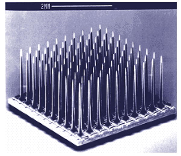
SEM photograph of the Utah Electrode Array.
As a power source of such neural interfaces, batteries are not suitable due to their limited lifespan, power density, and the geometric constraints of the envisioned neural interface device. Wireless power delivery through inductive coupling can be a solution to provide power to implanted devices [2]-[4]. It utilizes electromagnetic induction between two magnetically coupled coils and provides the device a virtually infinite lifetime. An efficient receiver coil needs to be designed to inductively power the neural interface over a certain distance. The technical requirements for these power coils are:
Maximum diameter: 5 mm
Minimum transmission distance: 5 mm
Transmission frequency: 2.64 MHz
Minimum voltage delivery: 4.5 Vpeak
Minimum power delivery: 10 mW
Besides the specifications listed above, the factors to be considered during the design and fabrication of such power coils are high inductance and quality factor of the coils, biocompatibility, and interconnection with other functional sub-components of the neural interface device.
In this study, coils to serve as a power source of the integrated neural interface were designed, fabricated, characterized, and finally its power transmission performance was tested in laboratory condition.
2 Design of Power Coils
The coils were designed to maximize the inductance and quality factor (Q) and to minimize the parasitic losses. When a coil has a high inductance, it needs only a low capacitance to resonate at a frequency, allowing the use of small-sized SMD (surface mounted device) capacitors or the integration of the capacitor into an IC. The higher the Q-factor of a coil, the higher the power it can receive. It is important to keep the parasitic losses as low as possible, to ensure the functionality of inductive power transmission in a certain range of operating frequency.
The dimensions of the UEA allow the maximum diameter of power coils to be 5 mm. Since a coil will have a maximum Q-factor when the opening in its center is 20-25 % of the coil diameter [5], the inner diameter of power coils was determined to be 1.25 mm. Other geometrical parameters such as the width, spacing, and height of coil turns were determined to achieve high number of windings within the technical limitations (e.g. minimum structure size, maximum aspect ratio achievable with thin film technologies) that still guarantee good fabrication quality. A trace width and spacing of 15 μm were considered as a feasible dimension for coil turns, with which a reasonable production yield was possible for coil thicknesses in excess of 10 μm. A 200 μm thick ferrite platelet was used to increase the Q-factor of coils as well as to protect the underneath electronics against electromagnetic interferences (see Fig. 2). Several different types of single- and double-layer coils were fabricated and tested for the power transmission.
Fig. 2.
Schematic of the cross section of single-layer and double-layer coils with a ferrite platelet underneath.
Stackable coils were proposed to avoid undesirable high inter-winding capacitance that may exist between coil layers in double-layered coils. An interconnection layout was devised to accommodate these stackable coils, allowing to switch between different coil configurations (see Fig. 3). The stacked coils can be switched in parallel or series to tune the coil parameters and therefore the resonant frequency of power transmission. With this feature, the layout can provide a certain degree of flexibility in coil configurations. Generally, micromachined MEMS devices do not allow easy changes in fabrication design, since high cost and time investments are required to change or modify the design of devices once a mask design is determined. For the initial stage of device development, however, a flexible configuration for the coil design was required such that the inductance and Q-factor of the coils, as a consequence, the resonance frequency can be modified. This allows compensating for unknown power signal variance due to the tissue and the placement accuracy of primary (driving) and secondary (receiving) coil.
Fig. 3.
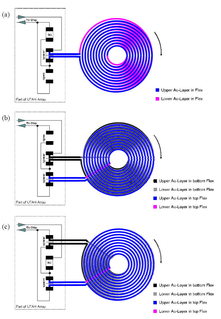
Switchable coil configuration using a single interconnection layout: (a) one double-layer coil, which can be replaced with one single-layer coil, (b) two stacked coils connected in series, (c) two stacked coils connected in parallel.
Fig. 4(a) shows the layout for interconnection of the coil, SMD capacitors, and the IC chip that is flip chip bonded on the backside of the UEA. Fig. 4(b) shows the schematic side view of the integrated neural interface device, in which all sub-components are electrically connected through the layout as shown in Fig. 4(a). Two spacers and a jumper are used to adjust the coils’ electrical characteristics to various parasitic capacitances and voltage gains. These spacers and jumper allow the operation of the coils in three different arrangements: 1) a single-layer or a double-layer coil, 2) two stacked coils connected in series, 3) two stacked coils connected in parallel (see Fig. 3).
Fig. 4.
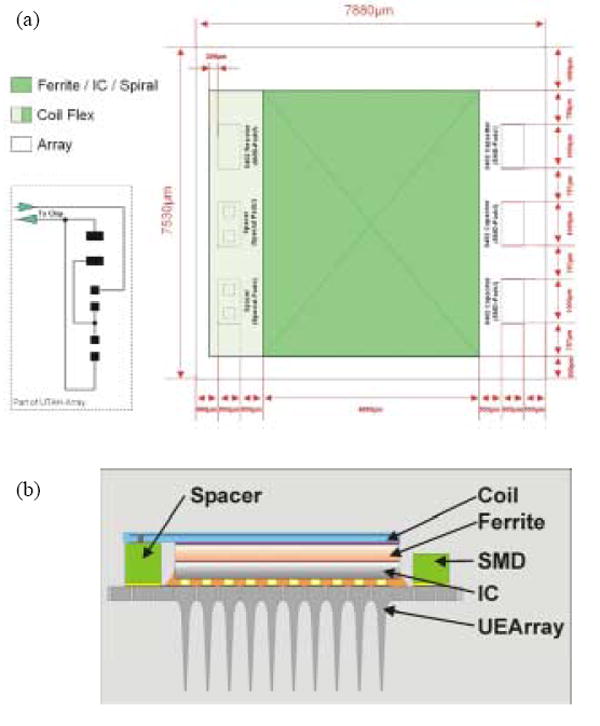
(a) Interconnection layout of the coil and other components. Two spacers and a jumper on the left side can be used for single or double coil assembly. The switchable interconnection plan is shown on the bottom left side. (b) Schematic of the cross sectional view of the integrated neural interface device.
3 Coil Fabrication
Taking into account simulation results [5], technological considerations, and the device assembly process [6], six different coil designs were manufactured. The coils were fabricated using the biocompatible materials such as gold and polyimide. To achieve sufficiently high density of coil turns within the given coil diameter, thin film technologies were used. Polyimide based Au coils were fabricated on a 4-inch silicon wafer. Each wafer carried 100 coils with different designs. Single- and double-layer coils were manufactured with line width and spacing of 15 or 20 μm, and the thickness of Au coil turns was approximately 10 μm.
Fig. 5 shows the schematic overview of the single-layer coil fabrication. First, a thermoplastic polymer, Staystik® 301 from AlphaMetals Inc., was spin coated onto a 4-inch silicon wafer to form a 15 μm thick release layer (Fig. 5(a)). This layer is necessary for the final separation of the thin film coils from the wafer. Next, polyimide, a polyamic acid type (PI 7320) from Fuji Film, was spin coated in a thickness of 15 μm. This PI layer serves as a base for the coils. As the adhesion layer and seed layer for electroplating, 100 nm TiW and 200 nm Au were sputter deposited (Fig. 5(b)). Photoresist (AZ 9000 from AZ Electronic Materials) was spin coated onto the sputtered metal layer, lithographically patterned, and developed (Fig. 5(c)). After electroplating 5 μm thick Au between the patterned photoresist, the photoresist was removed and the exposed plating base layer was etched (Fig. 5(d)). This first metal layer was created to lead the inner end of a coil to outside.
Fig. 5.
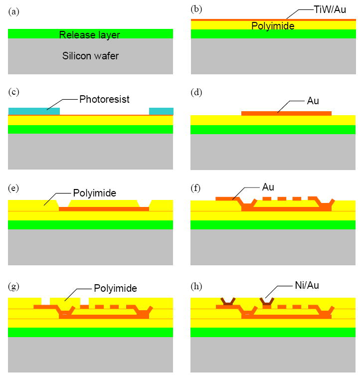
Schematic of the fabrication process of a single-layer coil.
Polyimide was again deposited to planarize the surface of the thin film stack of PI/Au for further fabrication steps. The vias connecting two subsequent metal layers were formed by lithography and developing unexposed part of polyimide (Fig. 5(e)). Here, the polyimide acts as a negative photoresist. To process the second metal layer that contains the coil turns, steps (b) through (d) were repeated (Fig. 5(f)). The third PI layer was deposited onto the Au/PI surface to protect the Au coil turns mechanically as well as electrically (Fig. 5(g)). This PI layer also contains vias for contact pads. 100 nm TiW and 300 nm Cu were sputter deposited as the seed layer to electroplate 5 μm Ni. Ni was chosen as the contact pad metal because of its wetting property, which can act as diffusion barrier when soldering. Afterwards, 100 nm Au was electroplated to prevent the oxidation of the Ni surface (Fig. 5(h)). Finally, individual coils can be diced and released from the silicon wafer by dissolving the release polymer layer.
For double-layer coils, the first metal layer of coil turns was formed by applying steps (b) through (d), replacing the connection lead from the inner end of coils to outside in case of single-layer coils. The first coil layer was connected with the second coil layer through the vias formed as described in steps (e) and (f).
Fig. 6 shows optical microscopic images of the electroplated Au coils with width and spacing of 15 μm. With this width and spacing, 60 turns could be realized on a layer. Fig. 7 shows an FIB (focused ion beam) image of the cross section of a single-layered coil as an example of the fabricated coils.
Fig. 6.
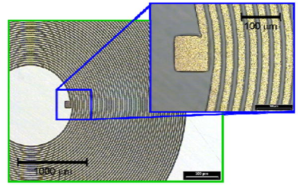
Optical microscopic images of an electroplated Au-coil on polyimide base layer.
Fig. 7.
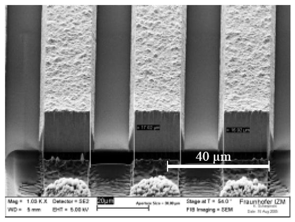
Focused ion beam (FIB) image of the cross section of a single-layer coil with 15 μm width and spacing.
4 Coil Characterization and Test
All six designs of the polyimide based coils were characterized with and without the LTCC (low-temperature-co-fired-ceramic) ferrite platelet backing. The coils were mounted on standard DIP40 ceramic packages for convenient testing. 3M multipurpose adhesive was used to glue the coils flat on to the LTCC platelet or to the DIP40 ceramic package. Aluminum wire of 25 μm in diameter was wire-bonded to connect the contact pads of the coils and the contact pads of the ceramic package, as shown in Fig. 8. The coils were mounted outside the cavity of the packages to avoid eddy currents associated with the conductive substrate in the cavity.
Fig. 8.
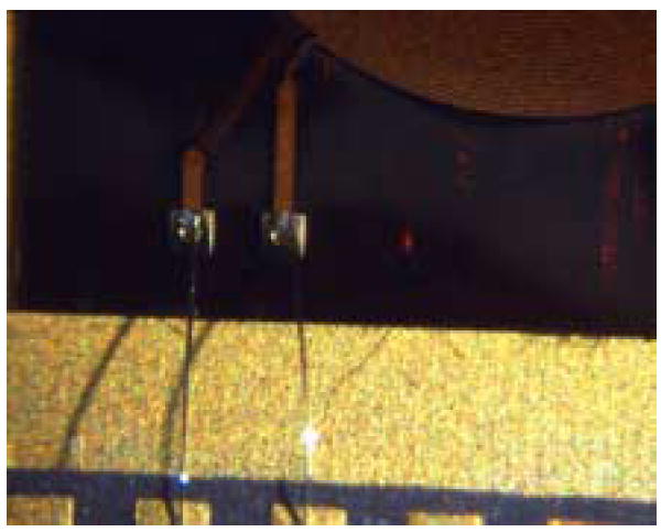
Photograph of a thin film PI/Au coil wire-bonded on a standard ceramic package for testing.
Inductance and resistance of coils were measured using a Stanford Research Systems SR715 LCR meter at 10 kHz. Because inductance and resistance are frequency dependant at high frequencies, the Q factor was measured empirically at the resonant frequency of 2.64 MHz, using the relation of Q = f0/BW, where f0 is the resonant frequency of 2.64 MHz and BW is the -3 dB bandwidth of the coil. This was accomplished by first selecting appropriate capacitors for each coil to resonate at f0. These capacitors were chosen empirically to avoid discrepancies due to parasitic capacitances in the test setup. A frequency sweep was then performed to determine the -3 dB point on either side of the peak impedance. BW is the difference between the two -3 dB frequencies. The frequency sweep was performed using an Agilent 33120A function generator with an amplitude of 10 Vpp. This supply has a fixed output source resistance of 50 Ω, which is comparable to the series resistance of the coils. Therefore, a 1 MΩ resistor was inserted in series with the coil to minimize the potential distortion of data due to frequency-dependant changes in coil inductance and resistance.
The measured electrical properties of each coil are shown in Table 1. Coil type A in Table 1 has 51 windings with a width of 20 μm and spacing between windings of 15 μm. Type B also has 51 turns, but with width/spacing of 15 μm/20 μm, and type C has 60 turns with width/spacing of 15 μm/15 μm. Single- and double-layer versions of three coil types make up the six geometries investigated. Each coil type was tested with and without ferrite backing, resulting in total twelve test configurations.
Table 1.
Measured electrical properties of the fabricated thin film Au coils.
| Coil Configuration | Measurements | ||||
|---|---|---|---|---|---|
| L (μH) | R (Ω) | Q @ 2.64 MHz | |||
| Single Layer | No Ferrite | A* | 7.29 | 33.5 | 2.49 |
| B | 7.41 | 40.5 | 2.18 | ||
| C | 10.3 | 50.5 | 2.78 | ||
| With Ferrite | A | 11.3 | 36.7 | 4.98 | |
| B | 12.1 | 40.0 | 4.80 | ||
| C | 16.9 | 50.5 | 5.08 | ||
| Double Layer | No Ferrite | A | 29.2 | 74.8 | 5.62 |
| B | 29.1 | 88.6 | 4.98 | ||
| C | 40.2 | 111.3 | 5.18 | ||
| With Ferrite | A | 46.9 | 74.5 | 9.10 | |
| B | 49.8 | 88.5 | 8.25 | ||
| C | 68.5 | 113.2 | 8.52 | ||
Coil Type A has 51 turns, winding width of 20 μm, and space between windings of 15 μm; Type B has 51 turns and width/spacing of 15 μm/20 μm; type C has 60 turns and width/spacing of 15 μm/15 μm.
For the same number of turns, coils of type B have more series resistance than those of type A. This is due to the smaller cross sectional area of the windings. Type C coils have more turns and thus have greater inductance and greater resistance. Double-layer coils had approximately four times the inductance of same type single-layer coils due to double the number of turns. The addition of the ferrite backing resulted in an average increase in inductance of 64 % without significantly affecting resistance. This led to an average increase in the Q factor of 82 %.
To test the power transmission to the fabricated thin film coils, a custom power transmitter was constructed (see Fig. 9). The power transmitting coil was a conventionally wound coil having a diameter of 12 mm. The voltage at this coil was limited at 80 Vrms. Each coil was tested using resonant capacitors to supply power to the electronics of the neural interface [7], which is currently packaged separately from the coil. The combined load of these electronics was about 3 mA. The left hand of Fig. 10 shows the power transmission test using a fabricated thin film PI/Au coil. The signals shown in the right hand of Fig. 10 are signals received at the PI/Au coil, rectified and regulated down to 3.3 VDC. It was found that higher inductance and higher Q coils were most effective for powering the electronics of the UEA. Approximately 4.5 V was required at the receive end to provide suitable headroom for a rectified and regulated 3.3 VDC power supply. All three double-layer, ferrite-backed coils were able to supply sufficient voltage to power the electronics at a distance of 8 mm. The type A coil was the most efficient, able to provide the necessary 4.5 V at a distance of up to 12 mm.
Fig. 9.
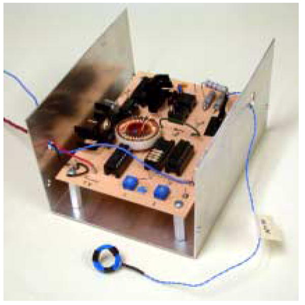
Custom-made power transmitter and power transmitting coil.
Fig. 10.
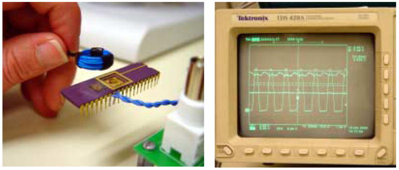
Experimental setup to test power transmission to a fabricated thin film PI/Au coil (left) and signals received at the coil, rectified, and regulated to 3.3 VDC (right).
5 Discussion and Conclusion
In this work, power coils to supply power to the integrated wireless neural interface devices were designed, fabricated, characterized, and its power transmission performance was tested in laboratory condition. The fabricated thin film Au coils based on a polyimide film can be switched between a single-layer, a double-layer, or two stacked coils with the help of a properly designed interconnection layout. The presented coils, based on a flexible polyimide film, are a stand-alone passive component and can be integrated in neural interface devices by soldering. With this feature, it can easily be integrated in other platforms as like in the Utah Electrode Array device provided the platform has proper contact pads and routing connections to other electronic components as presented in previous sections. This power coil is also used for forward data telemetry to transfer configuration/programming commands to the IC, while data transmission from the IC is being performed using a separate coil that is manufactured within the IC chip [7].
The most efficient coil type, a double-layer coil with 51 turns, width/spacing of 20 μm/15 μm, and a ferrite plate underneath showed an inductance of 46.9 μH and Q factor of 9.10 at 2.64 MHz, resulting in sufficient power supply to the electronics of the UEA, e.g. greater than 4.5 V over a distance of up to 12 mm. This exceeds the initial requirement of a power transmission distance of 5 mm minimum. All double-layered coils attached with ferrite platelet showed a Q of 8-9, which is considered to be moderate for the application. The Q can be increased by increasing the diameter and the number of windings of the coils if necessary, but very high Q coils are not desired in medical implant applications. The coils with a high Q have narrow bandwidths and as a result, the performance of the coils is highly sensitive to changes in coil’s resonant frequency. In implanted applications, small changes in inductance or capacitance of the implant coil can easily occur due to the presence of biological materials affecting the coil’s electrical parameters, which consequently causes detuning of resonant frequency. It is necessary to test power transmission using the thin film PI/Au coils in vivo with a fully integrated and encapsulated neural interface device.
Acknowledgments
This work was supported by NIH Neural Prosthesis Program, with the contract No. of HHSN265200423621C.
Footnotes
Publisher's Disclaimer: This is a PDF file of an unedited manuscript that has been accepted for publication. As a service to our customers we are providing this early version of the manuscript. The manuscript will undergo copyediting, typesetting, and review of the resulting proof before it is published in its final citable form. Please note that during the production process errors may be discovered which could affect the content, and all legal disclaimers that apply to the journal pertain.
References
- 1.Solzbacher F, Harrison R, Normann RA, Rieth L, Chakravarty S, Hsu J-M, Klein M, Oppermann H, Toepper M, Hahn R. NIH/NINDS Annual Neural Interfaces Workshop. Bethesda, MD, USA: 2005. A next generation chronically implantable wireless neural interface. Invited paper. [Google Scholar]
- 2.Akin T, Ziaie B, Najafi K. Digest, Solid-State Sensor & Actuator Workshop. Hilton Head, SC, USA: 1990. RF telemetry powering and control of hermetically sealed integrated sensors and actuators; pp. 145–148. [Google Scholar]
- 3.Hochmair ES. System optimization for improved accuracy in transcutaneous signal and power transmission. IEEE Trans on Biomedical Engineering. 1984;31:177–186. doi: 10.1109/TBME.1984.325404. [DOI] [PubMed] [Google Scholar]
- 4.Donaldson N, Zhou L, Haugland M, Sinkjaer T. Proceedings of the 5th Annual Conference of the International Functional Electrical Stimulation Society. Aalborg, Denmark: Jun 18-24, 2000. An implantable telemeter for longterm electroneurographic recordings in animals and humans; pp. 378–381. [Google Scholar]
- 5.Kim S, Scholz O, Zoschke K, Harrison R, Solzbacher F, Klein M, Toepper M. Proceedings of 2006 NSTI Nanotechnology Conference and Trade Show (Nanotech 2006) Boston, MA, USA: May 7-11, 2006. FEA Simulation of Thin Film Coils to Power Wireless Neural Interfaces. [Google Scholar]
- 6.Töpper M, et al. Proceedings of the 55th Electronic Components and Technology Conference (ECTC) San Diego, CA, USA: May 30 2, Jun 30 2, 2006. Biocompatible Hybrid Flip Chip Microsystem Integration for Next Generation Wireless Neural Interfaces. [Google Scholar]
- 7.Harrison RR, Watkins PT, Kier RJ, Lovejoy RO, Black DJ, Normann RA, Solzbacher F. Proceedings of 2006 IEEE International Solid-State Circuits Conference (ISSCC) San Francisco, CA, USA: 2006. A low-power integrated circuit for a wireless 100-electrode neural recording system; pp. 554–555.pp. 672 (Invited paper) [Google Scholar]


