

Abstract
A prototype Direct Detection Device (DDD) camera system has shown great promise in improving both the spatial resolution and the signal to noise ratio for electron microscopy at 120–400 keV beam energies (Xuong, et al., 2007. Methods in Cell Biology, 79, 721–739). Without the need for a resolution-limiting scintillation screen as in the charge coupled device (CCD), the DDD camera can outperform CCD based systems in terms of spatial resolution, due to its small pixel size (5 μm). In this paper, the modulation transfer function (MTF) of the DDD prototype is measured and compared with the specifications of commercial scientific CCD camera systems. Combining the fast speed of the DDD with image mosaic techniques, fast wide-area imaging is now possible. In this paper, the first large area mosaic image and the first tomography dataset from the DDD camera are presented, along with an image processing algorithm to correct the specimen drift utilizing the fast readout of the DDD system.
Keywords: Direct Detection Device, Active Pixel Sensor, image processing algorithm, electron tomography, cryo-electron microscopy, cryo-electron tomography
1. Introduction
Film has long been regarded as the gold standard for image recording for transmission electron microscopy (TEM). However, for automated and high throughput data acquisition in electron tomography and cryo-electron microscopy, a digital solution is needed. As such, the charge coupled device (CCD), which provides digital readout, has become a popular image recording option for these applications (Fan, et al., 2000).
However, due to radiation damage and signal saturation (Roberts, et al., 1982), CCDs cannot be placed in the direct path of the electron beam. A phosphorescent scintillation screen is required to convert the electron image to a photonic image that can be relayed to the CCD camera, either by fiber optics or a lens system. Unfortunately, the electron-to-photon conversion process in the scintillation screens generally limits the spatial resolution of CCD systems. Each incident electron will produce a footprint or scattering profile that is quite large: for 300 keV electrons, the footprint can have a full width at half maximum (FWHM) of about 30 μm for a reasonably bright scintillator screen. CCD camera spatial resolution is limited by the size of this footprint.
In the recent years, we have developed a custom CMOS detector, based on the Active Pixel Sensor technology (Milazzo, et al., 2005, Xuong, et al., 2004). The prototype Direct Detection Device (DDD) with 512 x 550 pixels and 5 μm pixel pitch was extensively tested and proven to be radiation tolerant for an accumulated dose of >3.3 x 10⁶ electrons/pixel, enough for several months of low-dose image acquisition (Jin, et al., 2007, Xuong, et al., 2007).
In this paper, the MTF of the DDD is measured and compared with the specifications of commercial scientific CCD camera systems. The first mosaic image and the first tomography dataset from the 512 x 550 pixel prototype DDD system are presented, along with an image processing algorithm designed to correct for specimen drift.
2. Materials and Methods
2.1 Direct Detection Device sensor chip
The sensor chip of the prototype DDD system is an Active Pixel Sensor that is designed for electron microscopy and fabricated in a standard TSMC 0.25 μm CMOS process. The sensor chip consists of a sensitive p- epitaxial layer (about 8 μm thick) between a p-well layer and a p++ substrate. Inside each 5 μm pixel is a diode formed by the interface between an n-well implantation and the p-epitaxial region, as well as three transistors that read out the charge collected on the diode. The effective fill factor is 100% because the epitaxial layer is continuous, beneath the thin readout circuitry that is transparent to incident high energy electrons (Xuong, et al., 2007).
Within the 8 μm epitaxial layer, a single incident electron will liberate a large number of excited electrons (about 1000 excited electrons for a single 300 keV incident electron). These excited electrons diffuse randomly through the epitaxial layer until they are collected by one of the pixel diodes. During the integration time, each pixel diode accumulates all the charges from the excited electrons. At the end of integration, the voltage values in the sensor array are read out and digitized by a peripheral supporting board, and transferred to the host computer for display and archival (Xuong, et al., 2007, Jin, et al., 2007).
2.2 Image collection
The prototype 512 x 550 pixel DDD system has 4 parallel analog outputs, connected to 4 parallel 12-bit Analog-to-Digital Converters (ADC) on the supporting electronics board, each sampling at 1.25 MHz. A single read of the entire sensor array takes 57 ms.
To reduce the fixed-pattern reset noise, we use a correlated double sampling (CDS) method. It employs two non-destructive reads after each sensor reset, where the accumulated charges in all the pixel diodes get cleared out. A CDS frame is then formed by subtracting the subsequent non-destructive reads. The subtracted difference is simply the charge integrated in the pixel diode during the time elapsed from the start of the first read to the start of the second read. This elapsed time is defined as the effective exposure time. For the results presented in this paper, the effective exposure time was 94 ms.
The DDD has limited dynamic range and a pixel will saturate after about 10–15 incident electron hits. However, thanks to the fast readout speed of the DDD system, this problem can be easily solved by dividing the total exposure time needed for enough dynamic range into multiple shorter exposures. By summing up the multiple exposed frames together, a digitally integrated image can be formed. A typical DDD image shown in this paper is a summed image from 200 CDS frames. The usage of such an image collection scheme also enables us to apply image processing algorithms on each individual short exposure frame before the summing step such as the near real-time correction of specimen drift that is highlighted later in this report.
2.3 EM Tomography data collection
Data for tomographic reconstruction was acquired using the single-axis tilt method. A series of images was obtained as the specimen was tilted in angular increments of 1º from −30º to +30º, about an axis perpendicular to the optical axis of the microscope with a computer-controlled goniometer. Each of these images represented a projection of densities in the specimen from a particular angle of view. The images were aligned and the volume was reconstructed using the software package IMOD (Kremer, et al., 1996).
2.3 Equipment
The DDD detector assembly, including the sensor chip, the supporting electronics board, and the Peltier cooling device, was mounted in a modified JEOL TEM film camera drawer, making it possible to install the system quickly in any JEOL electron microscopes. The temperature of the DDD sensor chip was maintained at −15 °C to minimize damage from radiation (Xuong, et al., 2007).
We used a JEM-2000 EX II microscope for the tomography dataset at 200 keV and a JEM-4000 EX microscope for the large area image mosaic at 300 keV.
2.4 Specimen preparation
Preparation of the mouse cardiac muscle specimen began with obtaining S129 mice that were deeply anesthetized by pentobarbital. They were then perfused and fixed with 2% paraformaldehyde and 2% glutaraldehyde in 0.15M sodium cacodylate buffer. After postfixation with the same fixative solution, samples were incubated in 0.8% potassium ferrocyanide mixed with 2% osmium tetroxide (OsO4) in 0.15M sodium cocadylate buffer. Tissues were incubated in 1% uranyl acetate (UA) and dehydrated with a series of ethanol, then embedded by Durcupan ACM (Electron Microscopy Sciences, PA, USA) in a vacuum oven.
2.5 Image Mosaic
The image shift control of the electron microscope optics was utilized to move the electron image around, allowing the DDD camera to capture a different area for each exposure. The shift control was carefully set up to ensure a 50% overlap between images, which was used for estimating relative image positions in the final mosaic.
The peak in the normalized cross-correlation function between the overlapping regions in every pair of adjacent images contained information of the relative position between the two images. By fixing the first image in a large canvas, all other images were translated according to the relative positions found in the previous step. A final mosaic image was then assembled. Only x, y translations were considered in the algorithm and no image blending was used for the final mosaic.
3. Results and Discussion
3.1 Resolution of the DDD detector
The Modulation Transfer Function (MTF) is a widely accepted way of describing the resolution of an imaging system. Here we used the edge method (Ruijter, et al., 1992, Weickenmeier, et al., 1995) to measure the MTF of the DDD detector.
A 1mm thick Al metal block was placed directly on and covered more than half of the sensor chip. The edge of the metal block was used to create a test step function. The orientation of the edge was slightly skewed to the pixel columns, and this geometry allowed the edge to be over-sampled without interpolation, using information from many rows of the image (Meyer, et al., 2000, Buhr, et al., 2003).
The 300 keV electron beam was spread out to create a uniform illumination on the DDD, 500 CDS frames from the DDD detector were collected and averaged to produce the edge image (a direct summing was used assuming that the metal edge would create the same shadow on all frames).
An area containing a very straight segment of the edge was selected for the MTF calculation (shown in Figure 1). For each row in the selected area, the transition position was calculated to subpixel precision using linear interpolation between the data points. A linear regression was then performed on the transition positions for each row, in order to get the edge line orientation. Using this method, it was found that in the selected area in Figure 1, the edge position changes 1 pixel for every 17 rows. The rows were re-aligned according to the edge position by shifting each row 1/17 of a pixel relative to the previous row. Averaging the rows that had been re-aligned yielded the over-sampled edge profile with a 1/17 pixel sampling distance.
Figure 1.
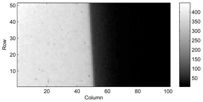
An image of the slightly skewed metal edge used for the MTF measurement at 300 keV. The image, a subset of 51 x 100 pixels, is an average of 500 frames (total dose: ~2000 electrons/pixel). The detector was maintained at −15 °C. Dark current, but not gain, correction was applied to the image.
The over-sampled edge profile showed a step transition, but also contained high frequency noise in the bright (high values) area caused by the large variation of signal generated by the incident electrons. To reduce the impact of the noise while retaining the edge transition profile, we adapted an analytical fitting method (Yin, et al., 1990) and used the sum of two sigmoid curves (Deptuch, et al., 2007) to fit the edge profile:
where y0 , g1,s1, g2 ,s2 ,a are fitting parameters and erf() is the error function.
The over-sampled edge profile is shown along with the fitted curve in Figure 2. Only the profile near the edge transition (10 pixels wide = 170 data points in the over-sampled profile) was used in the fitting. The edge spread function (ESF) and eventually the MTF were calculated using the fitted curve. To correct for the finite pixel size effect (Meyer, et al., 2000), the final MTF curve was divided by the sampling function (sinc function) based on the pixel size.
Figure 2.
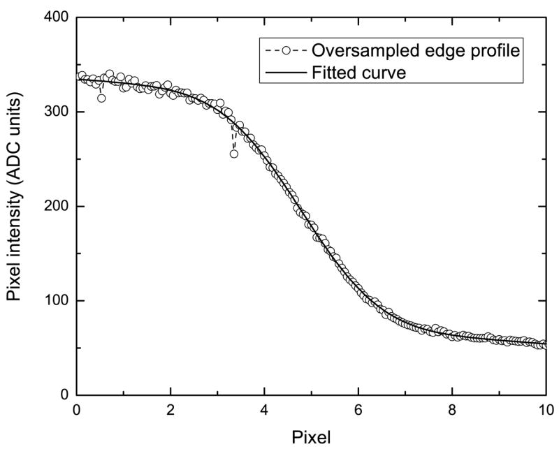
Over-sampled edge profile and the fitted curve using the sum of two sigmoid curves near the edge transition.
The resulting MTF curve for 300 keV electrons was shown in Figure 3a. At 1/2 Nyquist frequency (50 lp/mm), the DDD showed a MTF of >12%. Comparing to the publicly available MTF data for Gatan scientific CCD cameras and another active pixel sensor based detector, the MIMOSA V chip (Deptuch, et al., 2007), it is quite clear that the DDD outperforms other technologies at the same spatial frequencies. This advantage does not show up in a plot using the usual scale of 1/pixel (see Figure 3b). This is because, at Nyquist frequency, the MTF of the DDD degraded to a very low level. This degradation is believed to result from the scattering of incident electrons near the thin tip of the metal edge and also from the backscattering electrons re-entering the sensitive region of the detector at a different location other than the incident point, thus smearing out the edge profile. A detailed tabulated comparison with the Gatan scientific CCD cameras and the MIMOSA V chip is described in Table 1.
Figure 3.


a) MTF curve for the DDD at 300 keV calculated using the fitted curve in Figure 2. The finite pixel size effect has been corrected using a sinc function. At ½ Nyquist frequency (50 lp/mm), the MTF of the DDD is >12%. The DDD clearly outperforms other detectors at the same spatial frequencies.
b) The same MTF curves but shown using the usual scale of 1/pixel. The Nyquist frequency for any detector is now at 0.5/pixel and ½ Nyquist frequency is at 0.25/pixel. A detailed tabulated comparison is given in Table 1.
Table 1.
MTF comparison at ½ Nyquist frequency between the DDD, MV (MIMOSA V), and Gatan UltraScan CCD cameras. The MV data was taken from the published MTF curve from a front illuminated MV chip at 350 keV (Deptuch, et al., 2007). The Gatan Ultrascan 1000 and 4000 MTF values were obtained from the public datasheets from Gatan’s website*. Only 120 keV MTF values were available for the Gatan CCD cameras.
| Name | Pixel size | 1/2 Nyquist frequency (lp/mm) | MTF at 1/2 Nyquest | Method |
|---|---|---|---|---|
| DDD | 5 μm | 50 | >12% | Edge (300 keV) |
| MV (MIMOSA V) | 17 μm | 14.7 | >17% | Edge (350 keV) |
| Gatan UltraScan 4000 | 15 μm | 16.7 | >20% | Edge (120 keV) |
| Gatan UltraScan 1000 | 14 μm | 17.9 | >15% | Edge (120 keV) |
3.2 Large area image mosaic
The pixel pitch of the prototype DDD sensor is 5 μm, and it is one of the major advantages of the DDD systems over CCD systems. Although CCDs can have a pixel pitch of 15 μm or less, the resolution limiting factor is the large electron footprint in the scintillation screen. By comparing the images taken on a Tietz 2k x 2k TemCam-F224HD slow-scan 24 μm pixel CCD and the images taken on the DDD prototype using the same microscope magnification, it was clearly shown that the DDD image can contain 9 times the pixels in the CCD image for the same specimen area (Jin, et al., 2007, Xuong, et al., 2007). It indicates that to obtain similar specimen details, the microscope can be operated at much lower magnifications if the DDD is used instead of CCD.
The prototype DDD system has 550 x 512 pixels, and thus can capture a 2.75 mm x 2.56 mm region of the image formed at the film plane. Compared with a 2k x 2k CCD, the DDD camera captures only a small area in the center of the imaging field, but at a higher spatial resolution. The DDD system also benefits from the fact that the center of the imaging field has less distortion than the peripheral due to the imperfection of the projection lens of the microscope.
Using the image mosaic techniques described in the methods section of this paper, the DDD system can be adapted for wide area imaging, which is especially important for electron tomography of large scale biological structures.
As a demonstration, we took 44 images of a 500nm-thick section of mouse cardiac muscle tissue. By manually controlling the image shift of the microscope, each individual image captured a small area, with a 50% overlap region to adjacent images. The final mosaic (figure 4) was assembled after finding the relative positions between adjacent image pairs using normalized cross-correlation method. Although the microscope was operated at a low magnification of only 2500, the myosin bundles are clearly defined within the image and the much smaller actin thin filaments are observed near the Z line in the center region of the mosaic (figure 5).
Figure 4.
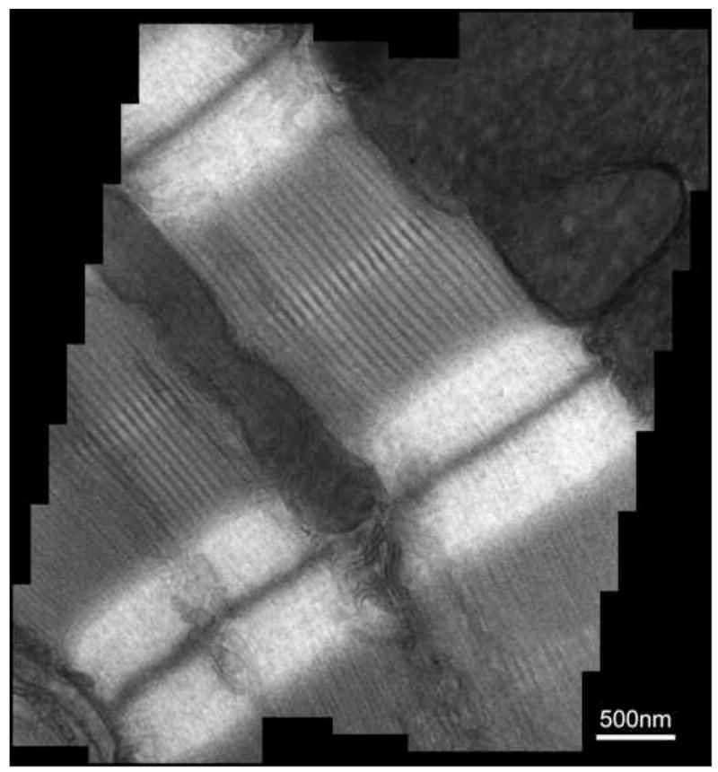
The mosaic image (~2k x 2k) of longitudinal mouse cardiac muscle specimen from 44 individual 512 x 550 pixel DDD images, each taken at 2500 magnification. For each image, the total dose is <200 electrons/pixel. The main features of the cardiac muscle, including the muscle Z line, myosin bundles and mitochondria, are clearly visible.
Figure 5.
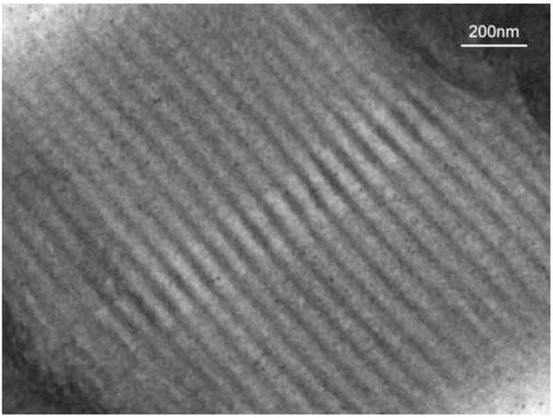
The center region of the muscle mosaic image of Figure 4, showing the thick myosin bundles and thin actin filaments near the Z line of the cardiac muscle. It illustrates the high resolution of this sensor at a relatively low magnification of 2500.
Since the image shift of the microscope can be easily computer controlled, the entire image mosaic acquisition can be automated and integrated into the process of tomographic data collection. For CCD systems, the same procedure can be used, but the number of images is limited by the range of image shift control. To go beyond the range of the image shift, microscope stage control can be used to further translate the specimen. However, using stage control can create unstable and unpredictable movements which are hard to correct. The waiting time for the stage to stabilize can also add a significant amount of time to the total acquisition for a large mosaic. For a DDD system with the same pixel counts as a CCD system with 15 μm effective pixel size at the same imaging plane, the same range of image shift control on the microscope will provide 9 times the imaging area, due to the small 5 μm pixel size of the DDD system.
3.3 Specimen drift correction
Specimen drift is usually observed in electron microscopes at high magnification. It is mostly due to the charging effect on the specimen surface during the beam illumination. The charge build-up can be drastically reduced if a conductive carbon coating is applied. However, even with the carbon coating, specimen drift is still observed and causes images to blur. It is even more of a problem for the DDD system, because the DDD image collection scheme depends on multiple short exposure frames. For a typical image from the 512 x 550 pixel DDD prototype, it will usually take about 50 seconds to collect all 200 short exposure frames. This collection time includes a 20-second total exposure, 20-second detector dead time and 10-second extra time for data streaming to the computer. Due to the size of the buffer on the supporting electronics board, usually a burst of 20 frames are collected, buffered, and then transferred to the computer before the next 20 frames are acquired. As an important note, the detector dead time and the limited image acquisition buffer are only the problems with this 512 x 550 pixel prototype system. In the next generations of the DDD system, both issues will be addressed.
Using the fast readout of the DDD, the specimen drift issue can be mitigated by using image processing techniques. From the 200 individual short exposed frames, specimen drift can be estimated using normalized cross-correlation method between subsequent frames. To reduce the noise impact on the accuracy of the cross-correlation method, each group of 5 sequential frames from the DDD is summed together and the summed images were then passed on to the cross-correlation procedure to determine the specimen drift direction and the relative pixel shift. These parameters were then used to align the summed frames and form the final corrected image.
Figure 6 shows a set of pixel shift parameters along the x and y directions of the detector. They were found in the cross-correlation procedure using the data from the large mosaic image. In this experiment, the specimen did not have a carbon coating, so the drift was quite large. The x-direction pixel shifts followed a linear relationship with the frame count, which is an indication of the time elapsed. The y-direction pixel shifts were close to zero, while the x-direction showed a significant drift over time.
Figure 6.
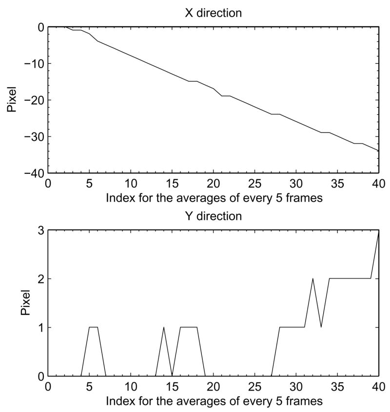
Estimated specimen drift amplitudes in both x- and y- direction of the imaging sensor, calculated using normalized cross correlation applied to the averages of every 5 sequential frames. The x-direction graph shows a substantial drift over time while the y-direction graph shows only slight deviations.
3.3 EM Tomography
To demonstrate the capability of the Direct Detection Device (DDD) for electron tomography, a dataset was collected using the mouse cardiac muscle specimen.
Using an EM magnification of 5000, a single tilt series of 61 images were taken at 1º increments from −30º to +30º. Each image underwent the specimen drift correction procedure before the alignment and reconstruction steps in IMOD. Due to the size of the prototype DDD detector, the number of gold fiducial particles was not enough for the fiducial alignment step, so only cross-correlation alignment and manual adjustment were applied.
Figure 7 shows a central x–y slice through the reconstructed volume. In this cross-sectional view of the cardiac muscle specimen, the myosin bundles appears as large black dots and the actin filaments are the small dots in between the large ones. Sarcoplasic reticulum (SR) is also shown as the linear double line structure on the lower left side and the mitochondria is at the top of the image.
Figure 7.
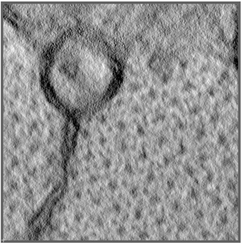
A central x–y slice through the reconstructed cross-sectional cardiac muscle tomographic volume. The total dose at each tile angle is <200 electrons/pixel. The large dots in the lower-right part of the image are the myosin bundles and the actin filaments are represented by the small dots in between the large dots. The linear structure in the lower left part of the image is sarcoplasic reticulum (SR) and it is connected to the mitochondria (at the top of the image) by a circular structure, which cannot be determined due to the limited size of the reconstruction.
By automating image mosaic acquisition at each tilt angle, the DDD system could be a useful tool for large scale structural studies.
3.4 Concluding remarks
In this paper, we presented the first large area image mosaic and the first tomographic dataset from a prototype Direct Detection Device system. Due to the small size of the prototype (512 x 550 pixels), the results here are more of a demonstration of principles. We now have a larger DDD with 1k x 1k pixels and will make detailed image comparisons with CCD based systems in the near future.
With the use of specimen drift correction and large area mosaic techniques, the DDD can increase the utility of electron tomography for studying large scale biological structures. The high sensitivity feature of the DDD was not emphasized in this paper, but it would make DDD suitable for many low-dose imaging applications such as cryo-EM and cryo-electron tomography (Milazzo, et al., 2005, Xuong, et al., 2007).
Acknowledgments
This research has been supported by NIH Grants RR018841 and RR004050. We thank Ron Quillin and Allen White for the electronics-related support, Masako Terada and James Obayashi for the tomography reconstruction assistance, and John Crum and Mason Mackey for microscope training and troubleshooting. We are grateful to Takeharu Hayashi and Andrea Thor for providing the mouse cardiac muscle specimen and to Ying Jones and Tom Deerinck for general specimen preparation assistance.
Footnotes
Publisher's Disclaimer: This is a PDF file of an unedited manuscript that has been accepted for publication. As a service to our customers we are providing this early version of the manuscript. The manuscript will undergo copyediting, typesetting, and review of the resulting proof before it is published in its final citable form. Please note that during the production process errors may be discovered which could affect the content, and all legal disclaimers that apply to the journal pertain.
References
- Buhr E, Günther-Kohfahl S, Neitzel U. Accuracy of a simple method for deriving the presampled modulation transfer function of a digital radiographic system from an edge image. Med Phys. 2003;30:2323–2331. doi: 10.1118/1.1598673. [DOI] [PubMed] [Google Scholar]
- Deptuch G, Besson A, Rehak P, Szelezniak M, Wall J, Winter M, Zhu Y. Direct electron imaging in electron microscopy with monolithic active pixel sensors. Ultramicroscopy. 2007;8:674–684. doi: 10.1016/j.ultramic.2007.01.003. [DOI] [PubMed] [Google Scholar]
- Fan GY, Ellisman MH. Digital imaging in transmission electron microscopy. J Microsc. 2000;200:1–13. doi: 10.1046/j.1365-2818.2000.00737.x. [DOI] [PubMed] [Google Scholar]
- Jin L, Milazzo AC, Kleinfelder S, Li S, Leblanc P, Duttweiler F, Bouwer JC, Peltier ST, Ellisman MH, Xuong NH. The Intermediate Size Direct Detection Detector for Electron Microscopy. Proc SPIE Int Soc Opt Eng. 2007;6501:65010A. [Google Scholar]
- Kremer JR, Mastronarde DN, McIntosh JR. Computer visualization of three-dimensional image data using IMOD. J Struct Biol. 1996;116:71–76. doi: 10.1006/jsbi.1996.0013. [DOI] [PubMed] [Google Scholar]
- Meyer RR, Kirkland AI. Characterisation of the signal and noise transfer of CCD cameras for electron detection. Microsc Res Tech. 2000;49:269. doi: 10.1002/(SICI)1097-0029(20000501)49:3<269::AID-JEMT5>3.0.CO;2-B. [DOI] [PubMed] [Google Scholar]
- Milazzo AC, Leblanc P, Duttweiler F, Jin L, Bouwer JC, Peltier ST, Ellisman MH, Bieser F, Matis HS, Wieman H, Denes P, Kleinfelder S, Xuong NH. Active pixel sensor array as a detector for electron microscopy. Ultramicroscopy. 2005;104:152–159. doi: 10.1016/j.ultramic.2005.03.006. [DOI] [PubMed] [Google Scholar]
- Roberts P, Chapman J, MacLeod A. A CCD-based image recording system for the CTEM. Ultramicroscopy. 1982;8:385–396. [Google Scholar]
- Ruijter WD, Weiss J. Method to measure properties of slow-scan CCD cameras for electron microscopy. Rev Sci Instrum. 1992;63:4314. [Google Scholar]
- Weickenmeier A, Nchter W, Mayer J. Quantitative characterization of point spread function and detection quantum efficiency for a YAG scintillator slow scan CCD camera. Optik(Stuttgart) 1995;99:147. [Google Scholar]
- Xuong NH, Milazzo AC, LeBlanc P, Duttweiler F, Bouwer J, Peltier S, Ellisman M, Denes P, Bieser F, Matis HS. First use of a high-sensitivity active pixel sensor array as a detector for electron microscopy. Proceedings of SPIE. 2004;5301:242. doi: 10.1016/j.ultramic.2005.03.006. [DOI] [PubMed] [Google Scholar]
- Xuong NH, Jin L, Kleinfelder S, Li S, Leblanc P, Duttweiler F, Bouwer JC, Peltier ST, Milazzo AC, Ellisman MH. Future Directions for Camera Systems in Electron Microscopy. In: Methods in Cell Biology. 2007;79:721–739. doi: 10.1016/S0091-679X(06)79028-8. [DOI] [PubMed] [Google Scholar]
- Yin FF, Giger ML, Doi K. Measurement of the presampling modulation transfer function of film digitizers using a curve fitting technique. Med Phys. 1990;17:962–966. doi: 10.1118/1.596463. [DOI] [PubMed] [Google Scholar]