

Abstract
Fabrication of metallic nanopillar array structures and their application as electrodes in electrochemical-based biosensors are discussed in this report. Vertically standing nanopillar array structures were fabricated using an electrodeposition technique and their electrochemical characteristics were evaluated. For possible use in biosensing applications, these standing nanopillars should have sufficient mechanical stability to sustain the capillary forces caused by the nanopillar – liquid interactions in aqueous environment and should provide increased signal response in an electrochemical process. Our results showed that the developed nanopillar arrays were mechanically stable in aqueous environments and the nanostructured electrodes exhibited increased electrochemical response compared with flat electrodes.
Keywords: nanopillar array structures, nanostructured electrodes, mechanical stability, electrochemical process, biosensors, porous anodic alumina
Introduction
Nanostructures such as nanorods, nanowires, nanotubes, and nanoparticles have attracted a lot of attention, as these structures show interesting optical, electrical, and mechanical properties. These structures have potential applications in nanoelectronics and nanobiotechnology. Recently, the use of vertically aligned nanostructures in biosensors has been explored. It has been reported that the use of carbon nanotubes (Wang et al 2002; Gao et al 2003; Wang and Mustafa 2003, 2004), peptide nanotube (Yemini et al 2005), and nanoparticles (Bharathi and Nogami 2001) in various biosensors increased signal detection. For example, electrodes modified with peptide nanotubes (Yemini et al 2005) showed a 2.5-fold increase in amperometric response compared with non-modified electrodes. Similarly, electrodes incorporated with carbon nanotube arrays (Gao et al 2003) showed a significant increase in selectivity and sensitivity in glucose sensing. Recently, nanoparticles have also been used to modify the bare electrode surface. For instance, surface plasmon resonance biosensors incorporated with gold nanoclusters (Chen et al 2004) increased detection resolution performance 10-fold.
A surface modified with vertically standing nanostructures has significantly greater surface area than a flat surface. Incorporating such a nanostructured surface into a sensing device will greatly increase the device’s active surface area without affecting its overall dimension. This feature makes these nanostructures attractive for possible use in various sensing devices. In most sensing devices, particularly electrochemical devices, the sensitivity depends mainly on the surface area of the electrodes (Zhang et al 1996; Bard and Faulkner 2001; Delvaux and Demoustier-Champagne 2003). For example, these nanostructures will be able to provide increased active surface area for enzyme loading in biosensors, thus leading to enhanced sensitivity (Zhang et al 1996; Delvaux and Demoustier-Champagne 2003).
To date, various nanostructures have been fabricated using chemical vapor deposition (CVD) (Lau et al 2003), physical vapor deposition (PVD) (Fan et al 2004), and template-based electrodeposition (Forrer et al 2000; Wang et al 2002; Xu et al 2004). Lately, evidence has emerged to reveal that the nanotubes and nanorods developed by CVD and PVD could not sustain the capillary forces generated by the nanostructure – liquid interaction (Lau et al 2003; Fan et al 2004). When vertically aligned nanostructures are exposed to a liquid environment, capillary forces will be generated between the vertically aligned nanostructures and the liquid medium (Kralchevsky and Nagayama 2000). If the forces are large, the nanostructures will deform or bunch together. For example, the nanorods fabricated by PVD in our lab deformed severely upon water contact as shown in Figure 1. Such deformation or bunching of vertically aligned nanostructures will reduce the magnitude of increase in the active surface area, which otherwise would have increased significantly due to the incorporation of nanostructures. This deformation in the nanostructures upon liquid interaction poses a serious problem for their application in functional biosensor devices because biosensors will have to be exposed to one or more aqueous environments. Therefore, to be useful as a component in a biosensor, these nanostructures need to have sufficient mechanical strength to overcome the capillary forces.
Figure 1.
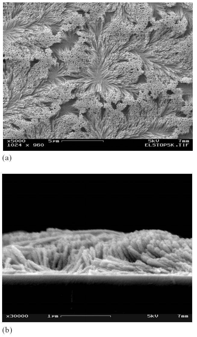
Deformed silicon nanorod arrays upon water exposure: top view (a) and cross section view (b). These nanorod array structures were fabricated using a glancing angle physical vapor deposition technique.
To address this issue, we developed an aqueous-based electrochemical deposition technique to fabricate vertically aligned standing nanostructures (nanopillars). This method has proved to be an elegant and cost-effective method in the fabrication of nanowires, nanorods, and nanopillars with various dimensions. The details of the deposition technique are discussed here and the electrochemical performance of the developed nanopillar array structures is reported.
Materials and method
To fabricate vertically aligned nanopillar array structures, we used porous anodic alumina (PAA) discs (Whatman Inc, UK) as templates and electrodeposited metallic materials through the pores of the PAA templates. Electrodeposition was conducted in a three-electrode system (1480 multistat, Solartron Corp, Houston TX, USA): a gold-coated PAA disc was used as the working electrode, platinum wire gauze was used as the counter electrode, and Ag/AgCl as the reference electrode. For gold nanopillar structures development, we used OROTEMP24 gold plating solution (Tehnic Inc, Cranston, RI, USA). Prior to electrodeposition of gold into the pores of the template, a thin layer of gold about 150 nm thick was sputter-coated on one side of PAA discs to provide a conductive coating, followed by electrodeposition of a thick gold film of approximately 3 μm on top of the sputtered coating in order to provide a strong supporting base to the nanopillar array structures. Then the supporting base was masked with Miccrostop solution (Tolber Division, Pyramid Plastics Inc, Hope, AR, USA) and gold was deposited into the pores of the PAA disc from the uncoated side under a constant current density of 5 mA/cm2 for 5 minutes at 65 °C. The height of the nanopillars can be controlled by varying the electrodeposition duration. The PAA template was then removed by dissolving it in 2.0 M NaOH solution. After the removal of the PAA template, vertically aligned gold nanopillar array structures on thick gold bases were obtained.
To assess the mechanical stability of these nanopillars qualitatively, a water droplet test was performed. (Note: a quantitative evaluation of mechanical stability of these nanostructures in aqueous environment is ongoing and will be reported separately.) The detail of the water droplet test was described elsewhere (Fan et al 2004). In brief, a water droplet was placed onto a nanopillar array structure and was allowed to dry for several hours. After that, the morphology of the nanopillars was examined under scanning electron microscopy (SEM) and compared with SEM images of the same nanopillar structure obtained prior to the water droplet test.
For evaluating the electrochemical characteristics of the developed nanopillar array structures, these structures were used as a working electrode (termed nanostructured electrode hereafter) and evaluated in a three-electrode electrochemical system. Cyclic voltammetry (CV) was performed on the nanostructured electrodes. As a control experiment, CV for flat gold electrodes having the same geometric area (about 16 mm2) was also performed. The flat gold electrode was prepared by depositing a thin film (300 nm) of gold on a titanium-coated glass plate using a thermal evaporator (built in house). To characterize the capacitive-charging behavior of the electrodes, CV was performed in 0.5 M Na2SO4 (a supporting electrolyte) at a scan rate of 100 mV/s; to evaluate the redox currents, CV was performed in 0.5 M Na2SO4 supplemented with 4 mM K4Fe (CN)6 (JT Baker Inc, Phillipsburg, NJ, USA) at various scan rates (50 mV/s, 100 mV/s, 150 mV/s, and 200 mV/s). All the tests were conducted in an unstirred solution and all solutions were prepared using high purity deionized water.
To assess the sensitivity of the nanostructured and flat gold electrodes in electrochemical sensing, the amperometric response of these electrodes was evaluated in 0.5 M Na2SO4 solution supplemented with K4Fe(CN)6 at 6 different concentrations (0.62 mM, 0.9 mM, 1.17 mM, 1.42 mM, 1.66 mM, and 1.89 mM) by measuring the transient current at a constant potential of 350 mV versus Ag/AgCl. The solution was stirred constantly during the amperometric experiments using a magnetic stirrer.
To characterize the morphology of the nanopillar array structures at various stages, namely, as deposited, before and after the water droplet tests, before and after the electrochemical tests, the morphology of the nanopillar array structures was examined under SEM.
Results and discussion
Figure 2 shows two SEM images of gold nanopillar array structures. These nanopillars have a diameter of about 150 nm and a height of 4.5 μm. These nanopillars exhibited slight bunching at their top ends. We believe that this bunching phenomenon can be attributed to the capillary interaction between the nanopillars and the electrolyte during the removal of PAA templates. These SEM images show that the morphology of the nanopillar array structures after the water droplet test (Figure 2b) is almost identical to that before the test (Figure 2a), indicating that the water droplet test did not further deform the nanopillar array structures.
Figure 2.
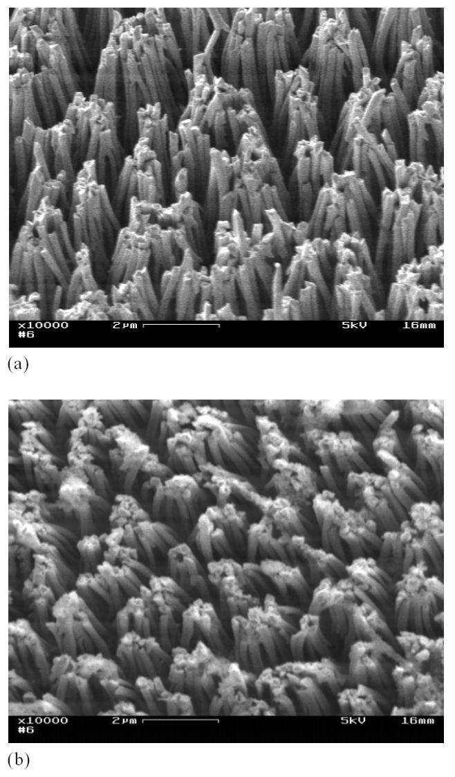
Gold nanopillar (aspect ratio = 30) array structures developed using electrodeposition: immediately after deposition (a) and after the water droplet test and several electrochemical test runs (b).
This type of deformation is quite different from the collapsing type deformation in the nanorods (see Figure 1) fabricated using PVD. Such a difference in nanostructure deformation suggests that the nanopillars fabricated by electrodeposition are much more mechanically stable than those fabricated using PVD.
In addition to the capillary interaction, we believe that the high aspect ratio of these nanopillars also contributed to their deformation. The nanopillars shown in Figure 2 have an aspect ratio of 30. Such a high aspect ratio will certainly reduce the bending resistance of the nanopillars. To verify this, we fabricated some nanopillar array structures with lower aspect ratios and subjected them to the same water droplet test. Figure 3 shows a silver nanopillar array structure with an aspect ratio of 10, before (Figure 3a) and after (Figure 3b) the water droplet test. Figure 4 shows a gold nanopillar array structure with an aspect ratio of 5, before (Figure 4a) and after (Figure 4b) the water droplet test. Clearly, neither nanopillar structure showed bunching or other deformations. These results indicate that the nanopillar array structures developed using the electrodeposition technique have sufficient mechanical stability to resist the capillary interaction forces in aqueous conditions.
Figure 3.
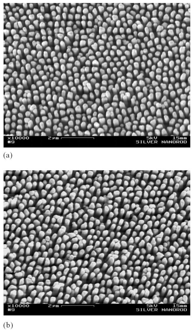
Silver nanopillar (aspect ratio = 10) array structures before (a) and after (b) the water droplet test.
Figure 4.
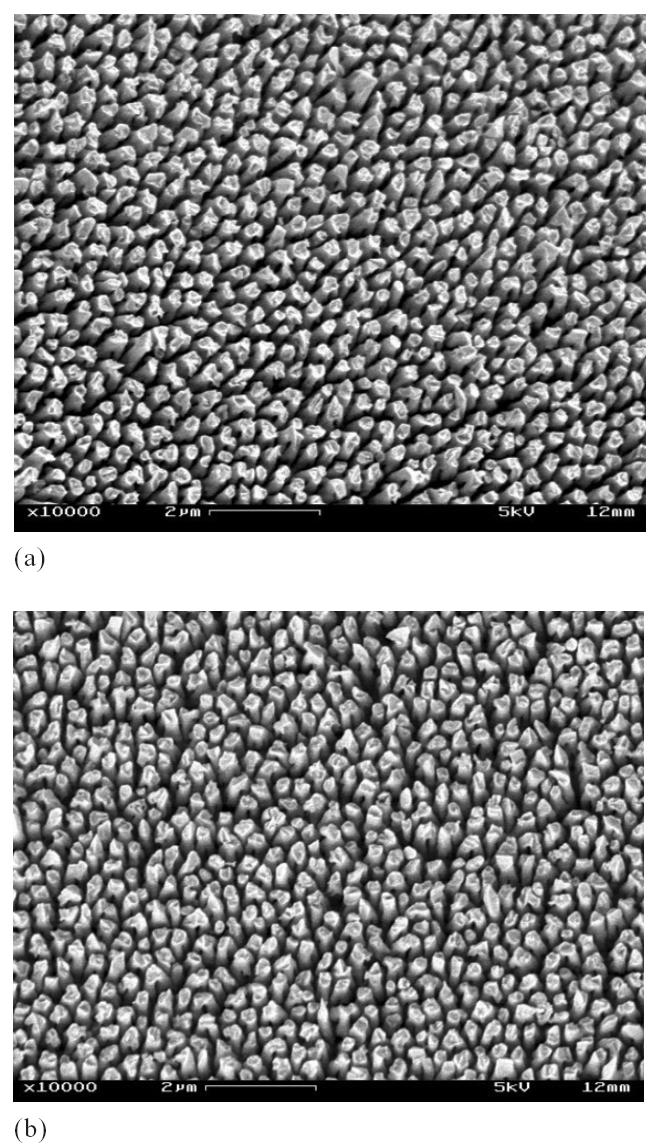
Gold nanopillar (aspect ratio = 5) array structures immediately after deposition (a) and after the water droplet test and several electrochemical test runs (b).
These nanopillars shown in Figures 1-4 have different diameters. But the question is: will such a difference affect the resistance of these nanopillars to capillary interaction? Considering a standing nanopillar as a cantilever beam with a point load (P, representing the net equivalent capillary force) acting on it, the deflection of the nanopillar (δ) can be expressed as δ = PL3/3EI (Beer et al 2002), where E is Young’s modulus of the material, L is the height of the nanopillar and I is the second moment of inertia (I = πD4/64, D is the diameter of the nanopillar). Obviously, the diameter of the nanopillar will affect the bending rigidity. However, according to Kralchevsky and Nagayama (2000), the capillary force generated at the nanopillar is proportional to the diameter of the nanopillar as P = K(γ,ϕ,δi)D, where K(γ,ϕ,δi) is a function of physical conditions such as the surface tension (γ), contact angle (ϕ), as well as the internanopillar distance (δi). Thus, the deflection of the nanopillar upon capillary interaction is proportional to the aspect ratio to the third power and inversely related to its Young’s modulus as δ ∝ (L/D)3/E. Therefore, besides these physical conditions, the aspect ratio of the nanopillars and their mechanical properties are important factors influencing the resistance of these nanopillars to capillary interaction. Since the values of Young’s modulus of amorphous silicon, gold, and silver are very close, ie, 80 GPa (Gardner et al 2002; Freund and Suresh 2003), 78 GPa, and 83 GPa, respectively (Gardner et al 2002), in this case only the physical conditions (the surface tension, contact angle, and internanopillar distance) and the aspect ratio will have dominating effects on the resistance of these nanopillars to capillary interaction.
Figure 5 shows the CV curves depicting the capacitive charging behavior measured in the supporting electrolyte at a scan rate of 100 mV/s for the flat (Figure 5a) and nanostructured (Figure 5b) gold electrodes. Clearly the nanostructured electrode showed a much higher charging current than the flat electrode.
Figure 5.
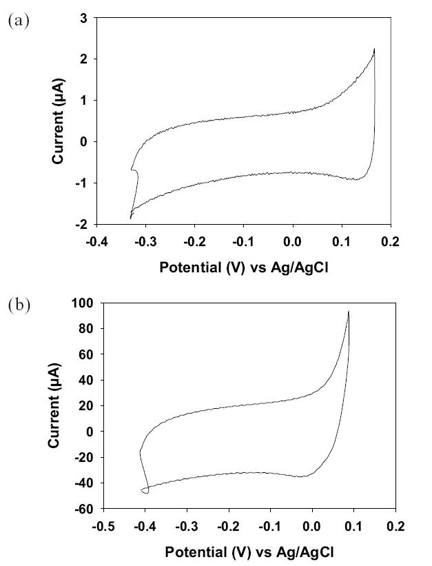
Cyclic voltammetry responses of a flat gold electrode (a) and nanostructured gold electrode (b). Both CV curves were measured in an electrolyte containing 1 M Na2SO4.
The charging current (ic) can be related to the electrolytically exposed area (A) by the following relationship (Forrer et al 2000):
| (1) |
where Cda is the double-layer capacitance per unit area and ν is the scan rate. In Figure 5, charging currents of 0.7 μA and 270 μA were recorded at −0.15 V (upper branch) for the flat and nanostructured electrodes, respectively. So, the charging current obtained for the nanostructured electrode is about 38 times higher than that for the flat electrode. Since gold is used as the electrode material in both the electrodes, the double layer capacitance per unit area can be assumed to be the same. Then, according to Equation 1, the electrolytically exposed surface area of the nanostructured electrode should be 38 times larger than that of the flat electrode. Geometrically, however, the surface area of the nanostructured electrode can be calculated using the formula: S0 + 2πnrl where S0 is the geometry area of the electrode, n is the total number of nanopillars in a given geometrical area, r is the radius of nanopillars, and l is the height of nanopillars. Based on this formula and SEM images, we estimated a 12-fold increase in the surface area of the nanostructured electrode compared with the flat electrode. This number is much smaller than the number (ie, 38) estimated based on Equation 1. A possible reason for such a discrepancy is that Equation 1 is developed based on the assumption that the double layer capacitance is independent of the applied potential, much like a regular capacitor. In reality, however, this is hardly the case (Bard and Faulkner 2001). This fact may imply that using charging current along with Equation 1 to estimate the electrolytically exposed area may not be a valid approach. Therefore, to be conservative we believe that a 12-fold increase in the electrolytically exposed area of nanostructured electrodes is more realistic.
Figures 6a and 6b show the CV curves of the nanostructured and flat gold electrodes measured in 0.5 M Na2SO4 supplemented with 4 mM K4Fe(CN)6 at various potential scan rates. The CV curves revealed that the redox peaks for the {Fe(CN)6}4−/{Fe(CN)6}3− couple and the peak currents increased with increasing scan rate. Also, the peak current for the nanostructured electrode was much higher than that for the flat gold electrode. Note that each of these CV curves represents 10 cycles of repeated measurement. Such a good reproducibility in repeated measurement suggests that the nanopillar array structures were very stable with no further deformation or change in morphology during the electrochemical process, which was confirmed by the SEM images after the electrochemical process. If these vertically aligned nanopillars are not strong enough to overcome the capillary forces in aqueous environment, they may deform or bunch during the electrochemical process, which would lead to decreased active surface area and hence decreased current output.
Figure 6.
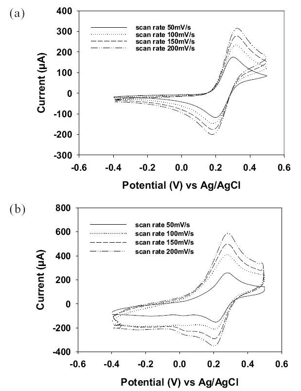
Cyclic voltammetry responses of gold flat electrode (a) and nanopillar array gold electrode (b) in an electrolyte containing 4 mM K4Fe(CN)6 and 0.5 M Na2SO4.
If the electrochemical process is a linear-diffusion-driven process, the peak current can be related to the active surface area (A) and the square root of the scan rate (ν1/2) by the Randles-Sevcik equation:
| (2) |
where n is the number of electron transfer, A is the active area of the electrode, C is the bulk concentration of the reactive species, D is the diffusion coefficient, and ν is the scan rate. By plotting the peak currents obtained at different scan rates against the square root of scan rate for both the nanostructured and flat electrodes, we observed linear relationships in both cases as shown in Figure 7. This suggests that the behavior of the electrochemical processes is indeed governed by a linear diffusion mechanism.
Figure 7.
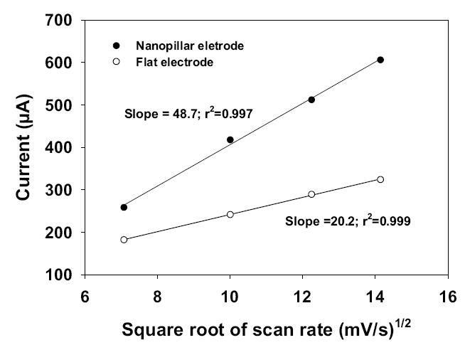
Variation of the peak current with the square root of scan rate (mV/S)1/2 in nanostructured and flat gold electrodes.
The amperometric current measured at different concentrations of K4Fe(CN)6 in 0.5 M Na2SO4 solution is shown in Figure 8a. It is evident that the amperometric currents obtained for the nanostructured electrode is significantly higher than the current obtained for the flat gold electrode. Plotting the steady state current measured at each concentration step against the concentration of K4Fe(CN)6 (Figure 8b) we observed that the steady state current is linearly related to the concentration of K4Fe(CN)6 for both types of electrodes. From Figure 8b, we calculated that the flat gold electrode has a sensitivity of 199.3 μA·mM−1·cm−2, whereas the nanostructured electrode has a sensitivity of 1451.8 μA·mM−1·cm−2, which is more than seven times higher. The high sensitivity in the nanostructured electrode can be attributed to the increased surface area due to the incorporation of those nanopillar array structures. This 7-fold increase in the sensitivity is very significant and will certainly lead to enhanced sensing capabilities in biosensors when their electrodes are incorporated with these nanopillar array structures.
Figure 8.

Amperometric responses (a) of gold nanostructured and flat electrodes in an electrolyte containing various concentrations of K4Fe(CN)6 in 0.5 M Na2SO4. Calibration curve (b) of steady state current versus the concentration of K4Fe(CN)6.
Conclusion
We demonstrated that the nanopillar array structures fabricated using an aqueous-based electrochemical deposition technique possess sufficient mechanical stability to resist the capillary interaction forces during the electrochemical processes and further aqueous exposures. In addition, a nanostructured electrode shows a 7-fold increase in its sensitivity compared with a flat electrode. Such a significant increase in the sensitivity of the nanostructured electrodes is attributed to the high surface area due to the nanopillar array structures. These aqueousbased electrodeposited nanopillar array structures can be used as viable structures for biosensor development for the purpose of enhancing the sensitivity of electrochemical-based biosensors.
Acknowledgments
This work was supported by the National Science Foundation (ECS-0304340) and University of Georgia Research Foundation through a Faculty Grant. The authors acknowledge Ms Xiaojia Tang for her experimental contributions.
References
- Bard AJ, Faulkner LR. Electrochemical methods: fundamentals and applications. New York: John Wiley; 2001. [Google Scholar]
- Beer FP, Johnston ER, Deworf JT. Mechanics of materials. 3. New York: McGraw-Hill; 2002. [Google Scholar]
- Bharathi S, Nogami M. A glucose biosensor based on electrodeposited biocomposites of gold nanoparticles and glucose oxidase enzyme. Analyst. 2001;126:1919–22. doi: 10.1039/b105318n. [DOI] [PubMed] [Google Scholar]
- Chen SJ, Chien FC, Lin GY, et al. Enhancement of the resolution surface plasmon resonance biosensors by control of the size and distribution of nanoparticles. Opt Lett. 2004;29:1390–2. doi: 10.1364/ol.29.001390. [DOI] [PubMed] [Google Scholar]
- Delvaux M, Demoustier-Champagne S. Immobilization of glucose oxidase within metallic nanotubes arrays for application to enzyme biosensors. Biosens Bioelectron. 2003;18:943–51. doi: 10.1016/s0956-5663(02)00209-9. [DOI] [PubMed] [Google Scholar]
- Fan JG, Dyer D, Zhang G, et al. Nanocarpet effect: pattern formation during wetting of vertically aligned nanorod arrays. Nano Lett. 2004;4:2133–8. [Google Scholar]
- Forrer P, Schlottig F, Siegenthaler H, et al. Electrochemical preparation and surface properties of gold nanowire array formed by template technique. J Appl Electrochem. 2000;30:533–41. [Google Scholar]
- Freund LB, Suresh S. Thin film materials. Cambridge, UK: Cambridge Univ Pr; 2003. [Google Scholar]
- Gardner JW, Varadan VK, Awadelkarim OO. Microsensors, MEMS, and smart devices. New York: John Wiley; 2002. [Google Scholar]
- Gao M, Dai L, Wallace G. Biosensor based on vertically aligned carbon nanotubes coated with inherently conducting polymers. Electroanalysis. 2003;15:13. [Google Scholar]
- Kralchevsky PA, Nagayama K. Capillary interactions between particles bound to interfaces, liquid films and biomembranes. Adv Colloid Interface Sci. 2000;85:145–92. doi: 10.1016/s0001-8686(99)00016-0. [DOI] [PubMed] [Google Scholar]
- Lau KKS, Bico J, Teo KBK, et al. Superhydrophobic carbon nanotube forests. Nano Lett. 2003;3:1701–5. [Google Scholar]
- Wang J, Mustafa M. Carbon nanotube screen-printed electrochemical sensors. Analyst. 2004;129:1–2. doi: 10.1039/b313431h. [DOI] [PubMed] [Google Scholar]
- Wang J, Mustafa M. carbon nanotube/Teflon composite electrochemical sensors and biosensors. Analyst. 2003;75:2075–9. doi: 10.1021/ac030007+. [DOI] [PubMed] [Google Scholar]
- Wang Z, Su YK, Li HL. AFM study of gold nanowire array electrodeposited within anodic aluminum oxide template. Appl Phys A. 2002;74:563–5. [Google Scholar]
- Xu J, Huang X, Xie G, et al. Study on the structures and magnetic properties of Ni, Co-Al2O3 electrodeposited nanowire arrays. Mater Res Bull. 2004;39:811–18. [Google Scholar]
- Yemini M, Reches M, Rishpon J, et al. Novel electrochemical biosensing platform using self-assembled peptide nanotubes. Nano Lett. 2005;5:183–6. doi: 10.1021/nl0484189. [DOI] [PubMed] [Google Scholar]
- Zhang Z, Liu H, Deng J. A glucose biosensor based on immobilization of glucose oxidase in electropolymerized o-aminophenol film on platinized glassy carbon electrode. Anal Chem. 1996;68:1632–8. doi: 10.1021/ac950431d. [DOI] [PubMed] [Google Scholar]