Abstract
A novel fabrication technique has been developed for creating high density (6.25 electrodes/mm2), out of plane, high aspect ratio silicon-based convoluted microelectrode arrays for neural and retinal prostheses. The convoluted shape of the surface defined by the tips of the electrodes could compliment the curved surfaces of peripheral nerves and the cortex, and in the case of retina, its spherical geometry. The geometry of these electrode arrays has the potential to facilitate implantation in the nerve fascicles and to physically stabilize it against displacement after insertion. This report presents a unique combination of variable depth dicing and wet isotropic etching for the fabrication of a variety of convoluted neural array geometries. Also, a method of deinsulating the electrode tips using photoresist as a mask and the limitations of this technique on uniformity are discussed.
Keywords: Micromachining, electrode arrays, dicing, wet isotropic etching, neural and retinal prostheses
1. Introduction
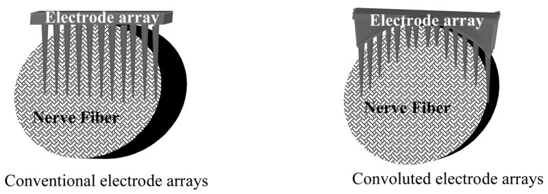
Microfabricated microelectrode arrays are used to record and stimulate neurons and nerve axons in the central and peripheral nervous systems. Advances in silicon micromachining have brought forth new configurations of microelectrode structures, such as the Utah Electrode Array (UEA), in either constant electrode length or varying length configurations [1–3]. Peripheral nerves have a cylindrical geometry, and the retina has a spherical geometry, so when conventional UEAs are implanted into these tissues, a gap will exist between the electrode array and the targeted tissue. This results in poor coupling to the tissue, and active electrode tips that are not in proximity to the neuronal tissue. For example, a constant length UEA (of size 4.2 × 4.2 mm2, and electrode length of 1.5 mm) when implanted in retina (radius of curvature = 12.5 mm) would result in a 170 μm gap between the retina and base of the center electrodes as shown in Fig. 1. Over time, this could result in a fibrotic tissue buildup between the array and nerve that might displace the array and potentially explant it from the nerve [4, 5]. Therefore, a conformal apposition to the tissue is important for signal recording, especially in chronic implantation. In the case of a retinal prosthesis application, the requirement of a snugly fitting electrode array is more severe not only because of the presence of high velocity saccadic eye movements but also because blind patients are often prone to falling and accidents.
Fig. 1.
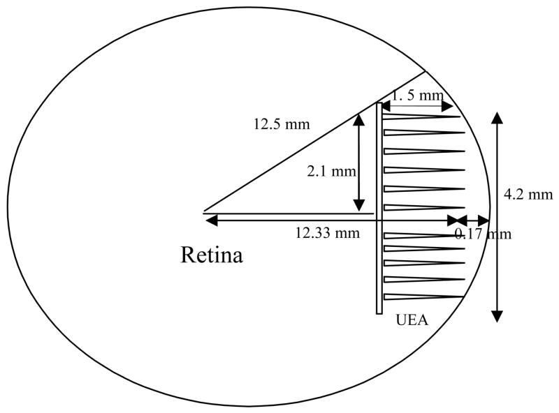
Cartoon image of constant length UEA implanted in retina highlighting the gap between the electrode array and the retina (note: drawing not to scale for clarity).
This report describes a novel method of fabricating electrode arrays with architectures that more closely conform to the cylindrical morphology of peripheral nerve fascicles, or the spherical geometry of the retina. Fig. 2 depicts the targeted shapes for the convoluted electrode arrays. The advantages of these geometries are: (1) the arrays would conform to the geometry of the nerves; (2) the variable height of the electrodes might improve the ability to selectively activate specific cortical lamina (curved due to the shape of the cortical gyri), or specific regions of the peripheral nerves; and (3) because their geometry conforms to that of the implanted tissues, these electrode arrays will minimize the extra-neural volumes that are present with conventional UEAs that could provide sites for fibrotic tissue ingrowth.
Fig. 2.
Targeted geometry for the silicon based convoluted electrode arrays.
This paper describes the design and fabrication of novel high density convoluted electrode arrays using variable depth dicing and wet isotropic etching. This is a maskless method for fabricating high aspect ratio microelectrode arrays. The different shapes which can be produced with this technique are highlighted in Fig. 3. The trough shaped electrode array could be used for recording and stimulating peripheral nerves, the spherical shaped electrode array is well suited for retinal prostheses applications, and the saddle shaped electrode array could be used in cortex. The radius of curvature of the surface created by the tips of the electrode array can be controlled by the cutting depth of the dicing saw depending on the application, as shown in Fig. 4. However, there are some limitations imposed by the dicing saw technique that restrict the different shapes of electrode arrays: for example, we can fabricate trough and saddle shaped electrode arrays however we cannot create a bowl shaped electrode array. Also, it is not possible to make the electrode lengths equal for some of the structures (B and D, specifically).
Fig. 3.
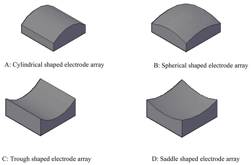
Cartoon image of different shapes of electrode arrays that can be achieved by variable depth dicing.
Fig. 4.
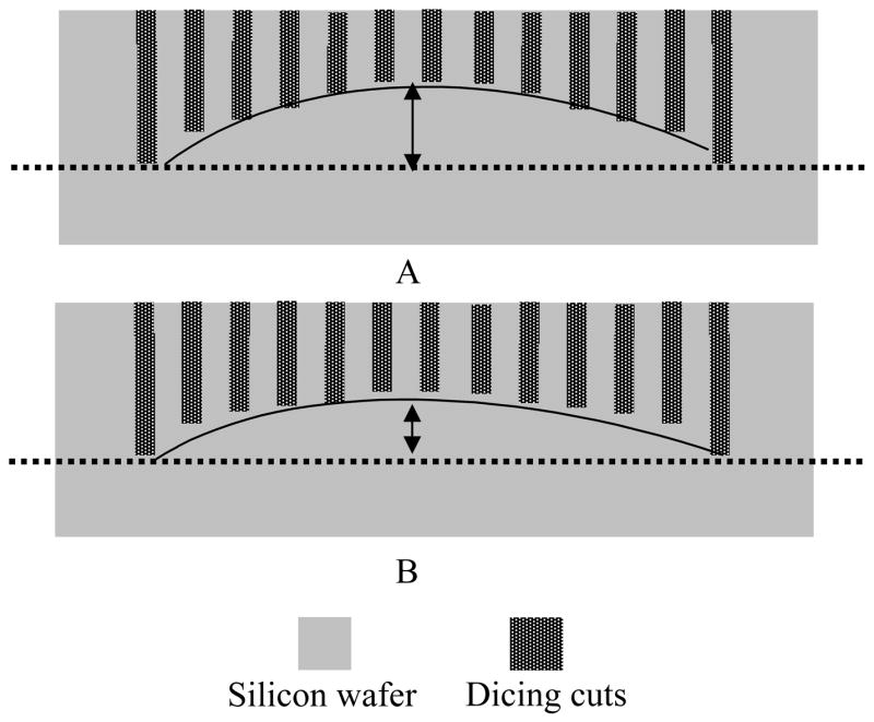
The curvature of the surface can be controlled by the depth of dicing saw. (A) dicing depth at the center is less than in (B).This will result in smaller radius of curvature in (A) compared to (B).
2. Fabrication Processes
2.1 Neural Electrode Array
Fig. 5 (A–J) illustrates the process flow for fabrication of convoluted shaped electrode arrays. The electrode arrays consist of a 10 × 10 matrix of 100 electrodes with varying height with the longest being 1.5 mm while the shortest is 0.5 mm, fabricated out of a 2 mm thick silicon wafer. The spacing between the electrodes in the array is 0.4 mm. In order to electrically isolate each electrode from its neighbors a dicing saw is used to make a 10 × 10 matrix of variable depth kerfs on the polished side of the wafer, Fig. 5B. Glass frit is then dispensed into these kerfs until the kerfs are completely filled. The glass is then melted in a furnace, Fig. 5C and the wafer is ground, lapped, and polished to a mirror finish, Fig. 5C. Electrical contacts are made to the back-side of each electrode using a Pt/TiW/Pt (240/480/670 nm) metalization scheme. The metalization layers are DC sputter deposited and photolithographically patterned on the polished surface, Fig. 5D. In order to form the initial electrode curvature, a dicing saw is utilized to make variable depth cuts indexed at 0.1 mm in the x and y directions on the non-polished side of the wafer, Fig. 5E. To fabricate the electrode columns, the dicing saw is again utilized to make a 10 × 10 matrix of variable height rectangular columns. This is done by making two sets of deep orthogonal cuts on the front side of the wafer, Fig. 5F. In order to form sharp electrodes, wet isotropic etching (HF 49 % + HNO3 69%) is performed on the diced wafer, Fig. 5G. The electrode tips are coated with a Ti/Pt/Ir (50/240/100 nm) metalization scheme that is sputter deposited on the tips to form an active electrode region, Fig. 5H. The electrode array is encapsulated with a biocompatible layer of parylene-C that is deposited by a chemical vapor deposition process (CVD), Fig. 5I. The Parylene-C insulation is then removed from the active tip area by a reactive ion etching (RIE) process using an inductively coupled oxygen plasma, Fig. 5J. Photoresist is used as a masking layer during the RIE.
Fig. 5.
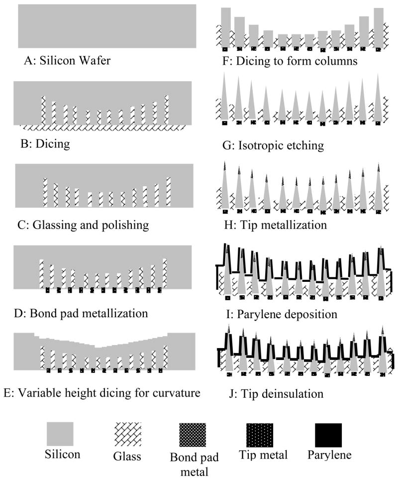
Process flow for fabricating saddle shaped neural electrode arrays.
2.2 Test Structure
Dicing
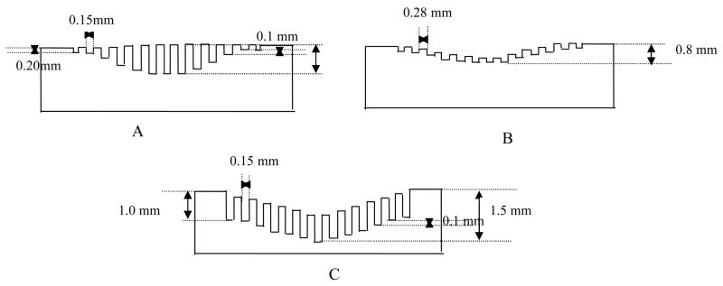
To develop test arrays, 2 mm thick, 75 mm diameter single crystal silicon wafers of 0.01–0.05 Ω-cm resistivity, (100) p-type were used. Neither the dicing of electrical isolation kerfs (Fig. 5B) nor the glassing (Fig. 5C) steps were performed for these test structures. Rather, a three step dicing process was used to create an array of rectangular columns, as shown in Fig. 6 (A–C). The first step, Fig. 6A, used a Disco, DAD 640, dicing saw to form the initial curvature. This process involved making a series of variable depth cuts with a pitch of 0.4 mm in one direction. The shallowest was 0.2 mm while the deepest cut was 0.8 mm. The silicon wafer was then rotated by 90°, and additional variable depth cuts were made with the same pitch. A 0.15 mm thick, 5 μm diamond grit size blade, with a 2 mm blade exposure rotating at 20,000 rpm was used to make variable depth orthogonal cuts into the silicon wafer. During the second step, a 6 μm diamond grit size blade with 0.28 mm blade thickness and 3.05 mm blade exposure was used to trim the columns formed in the previous step, as shown in Fig. 6B. This process produces the curvature in the silicon surface. To create the columns, thirteen cuts of variable depth were made with an index of 0.4 mm. The deepest cut being 1.5 mm and the shallowest cut being 1 mm. All these cuts were made with respect to the flat surface of the wafer. The wafer was then rotated by 90° and an additional thirteen cuts were made with the same parameters. The dicing blade thickness used in this step was 0.15 mm, Fig. 6C. The thirteen cuts yielded 10 rows of electrodes plus one extra row of electrodes on all four sides of the array. Apart from the extra row of electrodes, the fins and the corner posts were fabricated, as shown in Fig. 7. The extra row of electrodes, fins and the corner posts are designed to enhance uniformity in electrode geometry across the array during wet etching.
Fig. 6.
Process flow for dicing saddle shaped electrode arrays. (A) to define initial curvature, a 0.15 mm thick dicing blade was used to form variable height columns. 0.2 mm shallow cuts were made at the edge and 0.8 mm deep cuts were made at the center. The cuts were indexed at 0.1 mm. (B) to produce a curvature, a 0.28 mm thick dicing blade was used to trim the diced columns which were formed in step 6A. (C) to produce variable height columns, a 0.15 mm thick dicing blade was used. The shallowest cut was 1mm deep at the edge and the deepest was 1.5 mm at the center. The cut was indexed at 0.4 mm and was cut at an increment of 0.1 mm. All dimensions are with respect to the flat silicon wafer surface.
Fig. 7.
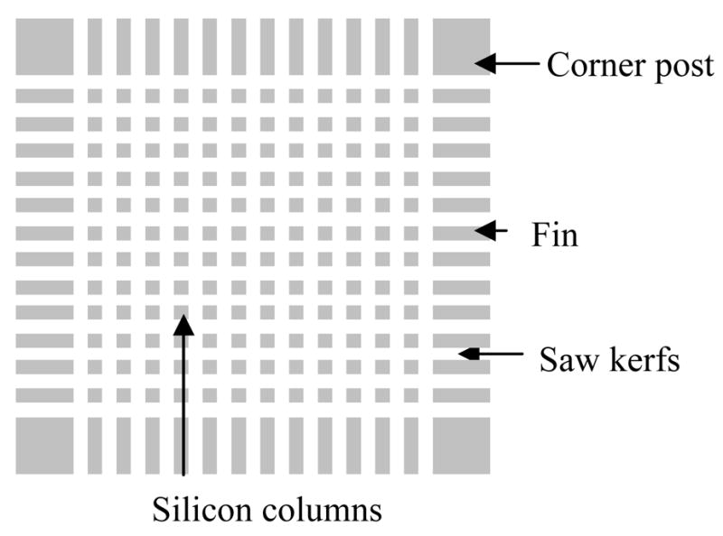
Top view of array after using a dicing saw to make deep orthogonal cuts into the Silicon wafer (schematic).
Etching
The rectangular columns are transformed into sharp electrodes using isotropic and anisotropic wet etching processes with a mixture of hydrofluoric acid (49% conc.) and nitric acid (69% conc.) in a ratio of 1:19 by volume. A 100 mm diameter Teflon wafer holder was developed for wafer-scale wet etching of these 75 mm diameter wafers [6]. The wet etching is a two-step process consisting of static and dynamic components; a detailed description of the etching procedures is given elsewhere [1, 6]. During the dynamic etching the wafer holder is rotated clockwise at 22 rpm while a magnetic stirrer is rotated counter-clockwise at 500 rpm, this stirs the acid aggressively. The wafer holder is placed in the etchant bath such that the top of the electrode columns are facing the magnetic stirrer. The holder attached to the motor is fixed at a distance of 5 cm from the bottom of etchant bath. The dynamic etching is carried out for 4 minutes and the rectangular columns are thinned and corners are rounded during this step. During the static etching the wafer holder is placed in the etchant with top of columns facing upwards, and neither the wafer nor the stir bar is rotated. The etching is carried out for 8 minutes and during this step the etchant preferentially etches the top of the column with respect to the base, resulting in sharpened tips. After etching, the fins and corner posts were trimmed using the dicing saw and the arrays were singulated into individual dies.
Tip metallization
In order to decrease the electrical impedance of the electrodes, the tips were metalized. A thin aluminum foil was used as a masking layer to protect the base of the device from sputtered metal. The aluminum foil was pierced by the electrodes to obtain the desired exposure [2, 3]. A metalization scheme of Ti/Pt/Ir (50/240/100 nm) was deposited on the tips of the electrodes by DC magnetron sputtering in a TM Vacuum SS-40C-IV multi cathode sputtering system. Argon was used as the process gas. The sputtering chamber was evacuated to 2 × 10⁻⁷ Torr before admitting Ar into the system. Titanium (99.5% pure), platinum (99.9% pure) and iridium (99.9% pure) of 3 inch diameter were used as the sputtering targets. The metal stack was deposited at 5 to 11 mTorr using power of 45 W for Ti and Ir and 90 W for Pt. The different sputtering parameters for different metals were optimized to minimize residual film stress. A -54 MPa compressive stress was measured in the optimized metal stack. The sputtering was performed at room temperature.
Insulation
The electrode array was then insulated with a biocompatible layer (Parylene-C). The insulation layer was deposited by a chemical vapor deposition process (CVD), a detailed description of which is given elsewhere [7]. Adhesion promoter, Silquest A-174® silane (GE Silicones, WV, USA), was applied on all the test arrays prior to Parylene-C deposition. Three μm thick Parylene-C films were deposited using a Paratech 3000 Labtop deposition system (Paratech Coating, Inc., CA, USA). Parylene-C dimer precursor was acquired from Cookson Electronics Equipment, USA. The dimer was vaporized at ~130 °C and subsequently pyrolized into reactive monomers at 670 °C. The test arrays were deposited at room temperature. The base pressure before Parylene dimer sublimation was less than 10 mTorr.
Deinsulation
The Parylene-C encapsulation must be removed from the active electrode tips so that contact can be made to neural tissue. This was done by using photoresist as a masking layer. Fig. 8 illustrates the process flow for deinsulation of the electrode array. A custom built Teflon holder was designed to hold the electrode arrays in a set of recesses. The depth of recess was greater than length of the electrodes. The electrode array was placed in the holder and the positive photoresist (AZ 4620) was spin coated (at 500 rpm for 20 sec) on the electrode array until all electrodes were submerged in the photoresist. The holder was placed in an oven at 50 °C for 10 hours to cure the photoresist. Parylene-C was removed from the active tip area by reactive ion etching the photoresist coated array in a capacitively coupled oxygen plasma (Oxford Plasmalab 80 plus). The dry etch used an oxygen flow rate of 50 sccm, etching pressure of 100 mTorr, and an RF power of 75 W at 13.56 MHz for 1.5 hours. Due to the high directionality of the plasma, etching starts from the tips of the electrodes. As the photoresist on tips of the electrodes was etched, the Parylene exposed to the oxygen plasma also gets etched thereby exposing the metal-coated electrode tips. The tip exposure is controlled by the etching time. The etch rate of Parylene for this process was 0.25 μm/min while that of photoresist was 0.18 μm/min. After etching the photoresist was removed from the electrodes with acetone.
Fig. 8.
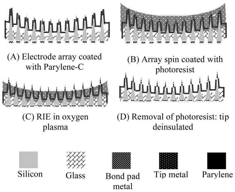
Process flow for de-insulating the electrode tips using photoresist as a masking layer.
3. Result and Discussion
Dicing
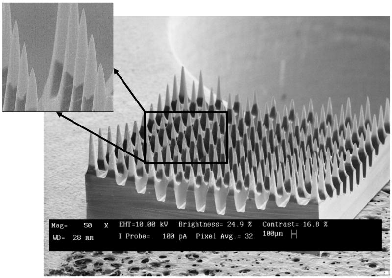
Fig. 9 shows an SEM micrograph of the electrode arrays after variable depth dicing (Fig. 5F). The SEM micrograph highlights the convoluted surface created by the tips of the rectangular electrode columns. The average tip width after dicing was 240 ± 15 μm. This variability in electrode dimensions across the wafer was due to the wearing of dicing blade.
Fig. 9.
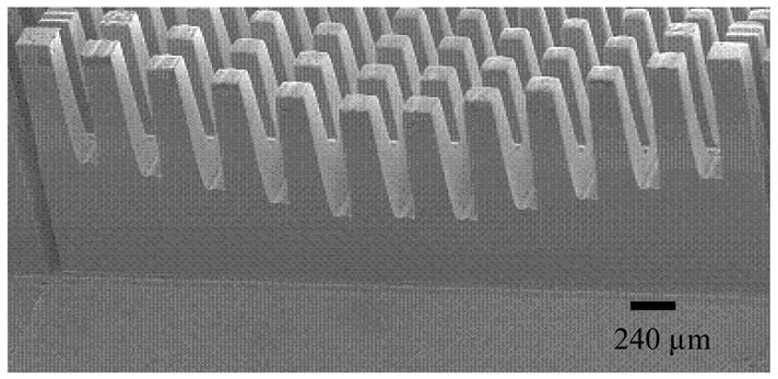
SEM micrograph of the side-view of an array after variable depth dicing.
Etching
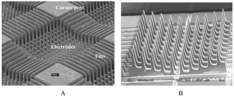
The objective of creating non-planar electrode arrays using the combination of variable depth dicing and wet isotropic etching has been achieved. The rectangular columns are uniformly etched into thinner columns (140 ± 20 μm) with rounded corners. The etch rate of silicon in acid was found to be 25 μm/min at room temperature. Fig. 10(A–B) presents an SEM micrograph of a saddle shaped electrode array after wet isotropic etching performed on wafer scale. Fig. 10B depicts a higher magnification image of Fig. 10A with a detailed view of the electrodes.
Fig. 10.
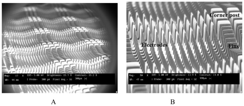
SEM micrograph of a saddle shaped electrode array after wet etching. (A) highlights the saddle shaped electrode arrays etched on wafer scale. (B) is zoom-in-view of one electrode array. The electrodes tips form a saddle shape, with corner post and fins at the periphery of the array.
Tip Metallization
The electrode arrays were transformed into functional devices by selectively metalizing the electrode tips using a thin (10 μm) Aluminum foil as a mask. Fig. 11 presents an SEM micrograph of a metalized array where a non-uniformity in tip metallization across the array was observed, resulting from the convoluted geometry of the array. The longer electrodes were metallized to a greater degree (more exposure through the Aluminum foil) than the shorter ones. The non-uniformity in tip metallization was not an issue because the entire array is insulated with Parylene-C and then the tips are selectively de-insulated, Fig. 5I and 5J.
Fig. 11.
SEM micrograph of electrode array after tip metallization.
Deinsulation
The deinsulation of convoluted shaped electrode arrays presents a challenge. Conventionally, for arrays having planar electrode tips, a thin Aluminum foil is used as a mask to deinsulate the constant electrode length (flat) and varying length (slant) configurations. This method is not feasible for deinsulating the convoluted shaped electrodes owing to their unique geometry. A photoresist based masking process was proposed to selectively etch and deinsulate the electrode tips, and Fig. 12 shows the results. The SEM image depicts the electrodes protruding out of the photoresist. Fig. 13 shows an SEM image of the electrode after the photoresist was removed in acetone.
Fig. 12.
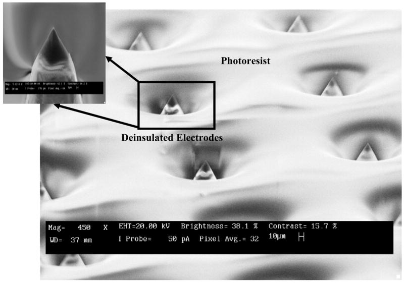
SEM micrograph of electrode array during tip deinsulation. Electrodes tips are exposed in the photoresist, as the photoresist is etched from the tips, Parylene also gets etched. Also shown is magnified image of a single electrode.
Fig 13.
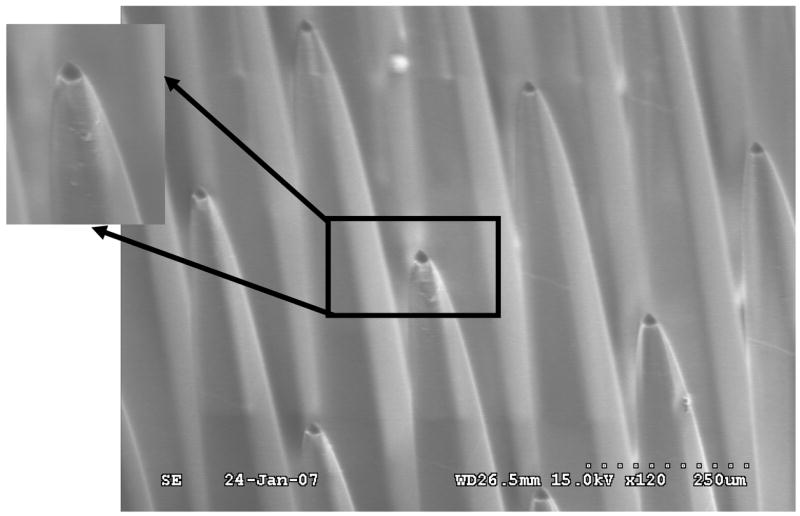
SEM micrograph of the electrode array after deinsulation.
The non–uniformity in electrode tip exposure across the array was measured by dicing and measuring one row of electrodes. The unique electrode geometry caused the tips of the longer electrodes to be exposed more (15 ± 5 μm) than the shorter ones (5 ± 3 μm). The variation in tip exposure will result in electrical impedance variability, leading to neural recordings with non-uniform signal-to-noise ratios across the array. Hence this method of deinsulation may not be ideal for such convoluted shaped electrode arrays. Further work will be required to refine the process, or develop a new process that can more uniformly deinsulate the electrodes in convoluted arrays.
The fabrication method described in this paper is a platform technology and can be extended to create a variety of different shaped electrode arrays. An example of a cylindrical shaped electrode array, having a curved surface in one direction and flat surface in the orthogonal direction, is shown in Fig. 14. Similarly, Fig. 15 shows an SEM micrograph of trough shape electrode arrays where one axis has a concave electrode surface while the other axis has a flat surface. These two electrode array geometries were produced using variable depth dicing in one direction and constant depth dicing in the orthogonal direction.
Fig. 14.
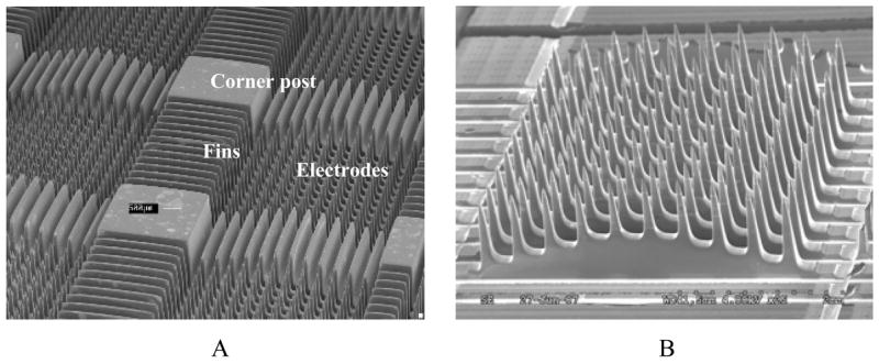
SEM micrograph of a cylindrical shaped electrode array are presented at two different magnifications and orientations. (A) presents the cylindrical shaped electrode array that was wafer-scale etched , depicting the electrodes, corner posts and fins along the edges. The center electrodes are longer than the ones at the edge. (B) shows an SEM image of an array after fins were trimmed and singulated by the dicing saw.
Fig. 15.
SEM micrograph of a trough shaped electrode array presented at two different magnifications. (A) shows the trough shaped electrode array that was wafer-scale etched showing the electrodes, corner posts and fins along the edges. In this array configuration the center electrodes are shorter than those at the edges. (B) shows an SEM image of an array after fins were trimmed and the arrays singulated.
4. Conclusions
This paper presents a novel array fabrication technique for building a variety of neural interface devices having complex three-dimensional geometries. The report describes a method to fabricate high aspect ratio, out-of-plane, convoluted shaped neural electrode arrays. A unique combination of variable depth dicing and wet isotropic etching was employed to fabricate novel geometries of convoluted electrodes for neural and retinal prostheses. These techniques have been used to create saddle, cylindrical and trough shaped electrode array geometries. A wafer scale wet isotropic etching method was used to etch 3-inch wafers. Also, a novel maskless technique for deinsulating variable tip exposures using photoresist was examined. However, because of variability in tip exposure, it was concluded that this technique may not be ideal for convoluted shaped electrode arrays and more work will be required to achieve uniform tip exposure.
Acknowledgments
This work was supported by NIH/NINDS (Contract No. HHSN265200423621C) and DARPA (Award No. 908164). The authors would also like to thank Jeremy Riley for his help in the dicing saw.
Biographies
Rajmohan Bhandari received the B.S. and M.S. degrees in physics from Garhwal University, Dehradun, India, in 1996 and 1998. In 2000 he received M.Tech. degree in physics from Indian Institute of Technology (IIT), Delhi-India, with majors in MEMS. He worked in a MEMS foundry in Singapore, as a Product Engineer, from 2001–2004. He worked as a Research Assistant in University of Calgary, Canada from 2004–2005. From 2005–2006 he worked as a Research Assistant in the Integrated Neural Interface Program (INIP) at University of Utah. Currently (2006-till date) he is pursuing PhD in ECE Department of University of Utah. His research interests include neural prosthesis, BioMEMS, biocompatible materials, and system integration.
Sandeep Negi received the B.S. and M.S. degrees in physics from Garhwal University, Dehradun, India, in 1996 and 1998, and the M.Tech. degree in physics from Indian Institute of Technology (IIT), Delhi, India, in 2000. From 2001 through 2004, he worked in MEMS industry in Singapore as a Product Engineer. From 2004 through 2005, he worked as Research Assistant in University of Calgary, Calgary, Alberta, Canada. From 2006 till date, he is working towards a PhD degree in the department of electrical and computer engineering at University of Utah, Salt Lake City, Utah, USA. He is a Research Assistant in the Integrated Neural Interface Program (INIP) at University of Utah and is researching the processes of charge injection at the stimulating electrode/tissue interface for the safe and efficacious neuroprostheses. His primary research interest includes the design, fabrication and testing of BioMEMS devices.
Loren Rieth received his B.S. degree in Materials Science from The Johns-Hopkins University, Baltimore, MD, in 1994. He received his Ph.D. in Materials Science and Engineering from the University of Florida, Gainesville, FL, in 2001. From 2001 to 2003, he was a Postdoctoral Research Associate at the University of Utah, Salt Lake City, UT, and continued on at the University of Utah as a Research Assistant Professor in Materials Science (2003–2005), and Electrical and Computer Engineering (2004–present). His research is focused on deposition and characterization of thin film materials for sensors (chemical, physical, and biological), MEMS, BioMEMS, and energy production.
Richard A Normann (M’88) received the B.S., M.S., and Ph.D. degrees in electrical engineering from the University of California, Berkeley. He joined the staff of the National Institutes of Health (NIH), Bethesda, MD, in 1974 and in 1979, he joined the faculty at the University of Utah, Salt Lake City. He is currently a Professor of Bioengineering and Ophthalmology. His research interests are parallel information processing in the vertebrate visual system and neuroprosthetics (the development of functional interfaces to the central and peripheral nervous system that can be used to restore lost sensory or motor function).
Florian Solzbacher received his MSc in electrical engineering from the Technical University Berlin in 1997 and his PhD from the Technical University Ilmenau in 2003. He is Director of the Microsystems Laboratory at the University of Utah and a faculty member in the Departments of Electrical and Computer Engineering, Materials Science and Bioengineering. and he is responsible for the Utah branch office of the Fraunhofer IZM, Germany. Dr. Solzbacher is co-founder of First Sensor Technology GmbH, an established supplier to the automotive and process control industry in the USA, Europe and Asia. He is Chairman of the German Association for Sensor Technology AMA. His work focuses on harsh environment microsystems, sensors and materials. He is author of over 60 scientific and engineering publications and book chapters on MEMS devices, technologies and markets for Harsh Environments. Since 2004 he has been Chairman of Sensor + Test, the world’s largest international trade fair and ensemble of conferences for sensors, metrology and testing.
Footnotes
Publisher's Disclaimer: This is a PDF file of an unedited manuscript that has been accepted for publication. As a service to our customers we are providing this early version of the manuscript. The manuscript will undergo copyediting, typesetting, and review of the resulting proof before it is published in its final citable form. Please note that during the production process errors may be discovered which could affect the content, and all legal disclaimers that apply to the journal pertain.
References
- 1.Campbell PK, Jones KE, Huber RJ, Horch KW, Normann RA. A Silicon–Based, Three Dimensional Neural Interface: Manufacturing Processes for an Intra cortical Electrode Array. IEEE Transaction on Biomedical Engineering. 1991 August;38(38):758–768. doi: 10.1109/10.83588. [DOI] [PubMed] [Google Scholar]
- 2.Jones KE, Campbell Patrick K, Normann Richard A. A Glass/Silicon Composite Intra cortical Electrode Array. Annals of Biomedical Engineering. 1992;20:423–437. doi: 10.1007/BF02368134. [DOI] [PubMed] [Google Scholar]
- 3.Branner A, Stein RB, Fernandez E, Aoyagi Y, Normann RA. Long term stimulation and recording with a penetrating microelectrode array in cat sciatic nerve. IEEE Transactions on Biomedical Engineering. 2004;51(1):146–157. doi: 10.1109/TBME.2003.820321. [DOI] [PubMed] [Google Scholar]
- 4.Edell DJ, Toi V, McNeil VM, Clark D. Factors influencing the biocompatibility of insertable silicon microshafts in cerebral cortex. IEEE Trans Bioemed Eng. 1992;39:635–643. doi: 10.1109/10.141202. [DOI] [PubMed] [Google Scholar]
- 5.Beard RB, Hung BN, Schmukler R. Bio-compatibility considerations at stimulating electrode interface. Ann Biomed Eng. 1992;20:395–410. doi: 10.1007/BF02368539. [DOI] [PubMed] [Google Scholar]
- 6.Bhandari R, Negi S, Rieth L, Toepper M, Normann RA, Solzbacher F. Wafer Level Processing Of Silicon Arrays for Implantable Medical Devices. Proceedings ECTC 2007; Reno, Nevada. [Google Scholar]
- 7.Hsu JM, Rieth L, Kammer S, Koch KP, Normann RA, Solzbacher F. PECVD a-SiC:H and Parylene encapsulation for chronically implanted neural recording devices. NIH/NINDS Neural Interfaces Workshop; Bethesda, MD. Sep 7–9, 2005. [Google Scholar]


