Abstract
This communication describes the fabrication of gold structures (for example, rings) with wall thickness of 40 nm, and with high aspect ratios up to 25. This technique combines thin-film deposition of metal on a topographically patterned epoxy substrate, with nanometer-scale sectioning using a microtome in a plane parallel to the patterned substrate. The dimensions of the metal structures are determined by the thickness of the metal film and the thickness of the epoxy sections. The shape of the resulting nanostructure is defined by the cross-section of the original template.
This paper describes the fabrication of gold nanostructures with high aspect ratios using a combination of thin film deposition and a recently developed technique based on sectioning with a microtome (which we call “nanoskiving”).1 The dimensions of the resulting nanostructures are controlled by the thickness of the metal film and the thickness of the epoxy sections. The shape of the nanostructure is defined by the geometry of the template.
High aspect-ratio microstructures have been used as the building blocks in a number of areas, such as microelectromechanical systems (MEMS),2,3 two-dimensional subwavelength photonic bandgap (PBG) devices,4–6 and sensors. Devices for high frequencies based on diffraction (e.g. Fresnel zone plates and diffraction gratings) and on refraction (e.g. wave plates and retarders) require both nanoscale dimensions and high aspect ratios for optimal operation.7 A number of techniques have been developed to fabricate high aspect ratio micro- and nanoscale structures; these include X-ray LIGA,8,9 deep reactive-ion etching (DRIE),10 focused ion-beam etching,11–13 and glancing-angle deposition (GLAD).14,15 These techniques are, however, not conveniently available to general users. Simple and inexpensive techniques to fabricate nanostructures with high aspect ratio are highly desirable.16
The microtome has been used extensively for preparation of thin samples for imaging with optical or electron microscopy.17,18 A microtome can generate polymer sections as thick as ~10 μm with a rotary microtome system, and as thin as 10 nm when equipped with an oscillating diamond knife.19 We have demonstrated previously the fabrication of conductive nanoelectrodes and nanowires based on thin-metal-film deposition and microtome sectioning using an ultramicrotome with a diamond knife.1,20 Here we used a similar technique but with a different topography, to fabricate high aspect-ratio gold nanostructures of types that would be difficult or impossible to obtain by conventional lithographic techniques.
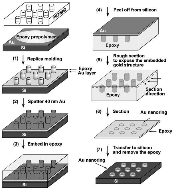
Figure 1 shows the procedure used to fabricate 3D, free-standing metal nanostructures by thin film deposition and nanoskiving. First, we used standard soft-lithographic techniques to fabricate a PDMS replica of an array of micro-posts patterned in S1813 photoresist.16,21 We then transferred these micro-posts onto epoxy (Araldite 502) by curing a layer of epoxy prepolymer against this PDMS stamp (step 1), using a gold-coated Si/SiO2 wafer as substrate. (The gold layer on the substrate facilitated the separation of the molded epoxy from it.) After peeling off the PDMS, we sputtered ~40 nm gold directly on the epoxy substrate (step 2). Non-collimated metal deposition ensured the formation of thin films on all surfaces of the epoxy substrate, including the sidewalls. We then embedded the gold-coated epoxy substrate in the same epoxy prepolymer (step 3). In order to facilitate mounting the sample in the sample holder of the microtome, this epoxy layer was intentionally made ~ 1 cm thick. After curing, we peeled the block of epoxy, together with the gold sacrificial layer, from the silicon substrate (step 4).
Figure 1.
Schematic illustration of the procedure used to fabricate gold nanostructures with a controllable size by a combination of thin metal film deposition and microtome sectioning in a direction parallel to the patterned epoxy surface.
To section the epoxy block in a plane parallel to the patterned surface, we used a microtome mounted with a diamond knife (Diatome, 45° knife angle), with water in the sample-collecting boat (steps 5 and 6). The edge of the knife and the plane of the sample must be aligned carefully to obtain uniform slices over a large area; this alignment is difficult, and the most time-consuming part of the procedure. It takes about 2 seconds to slice a single structure with a cross-sectional area of 500 μm × 500 μm; sectioning can, thus, generate a large number of nanoslabs rapidly, once the alignment is accomplished. Each epoxy section contains the embedded gold nanostructures; these nanostructures have their dimensions defined by i) the dimensions of the PDMS stamp; ii) the thickness of the deposited layer of gold; and iii) the thickness of the slab cut by the microtome.
We transferred these thin epoxy sections onto a silicon substrate by submerging the substrate in the water in the trough and pulling it back carefully in a way that allowed the floating polymer film come to rest on the Si/SiO2 substrate (step 7). We then removed the polymer matrix (epoxy) by etching with an oxygen plasma; this process left the gold nanostructures intact on the silicon substrate. (See supporting Figure 1)
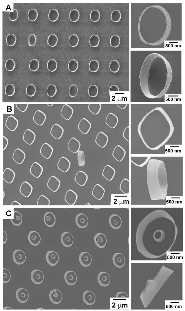
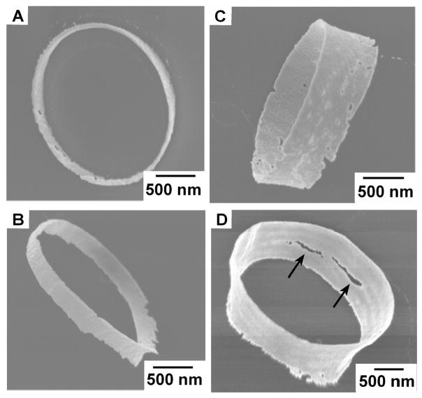
The SEM images in Figure 2 show nanostructures with different geometries fabricated by this procedure. These structures have walls ~40-nm thick and 500-nm high. The shape of the nanostructures showed some deformation relative to that of the original template (e.g. in Figure 2B, the nanostructures are approximately parallelograms, while the shape of the template was square). We attribute this distortion to the compression that the knife exerts on the sample during sectioning.18 An oscillating diamond knife would minimize the compression of the knife.18 A useful attribute of nanoskiving as a fabrication technique is that it can easily generate epoxy sections with thicknesses ranging from 30 nm to 10 μm;1 this flexibility makes it possible to tune the aspect ratio of the nanostructures by changing the thickness of the section. Figure 3 shows ring-shaped nanostructures having the same wall thickness but different heights. In order to illustrate the height of the structures, we intentionally picked for imaging nanorings that happened to have flipped onto their side. We attribute the defects on the nanostructures (as indicated by the arrows in the figure) to non-uniform deposition of the metal film and/or mechanical stress during sectioning.
Figure 2.
SEM images showing patterned free-standing gold nanostructures on a silicon substrate after removing the epoxy with oxygen plasma at 0.9 Torr, 70 W for 20 min. The wall thickness and the height of the ring are about 40 nm and 500 nm respectively. (A) Ring; (B) square; (C) double ring. (In each set: the left image shows large arrays of gold nanostructures with different shapes; the top-right image shows the top view of the free-standing nanostructures; the bottom-right image shows the top view of the nanostructure lying on the silicon substrate on its side to indicate the height of the wall.)
Figure 3.
SEM images of nanorings with different aspect ratios. The thickness of the wall is ~40 nm for all the nanorings; their heights are: (A) 70 nm, (B) 200 nm, (C) 500 nm, (D) 1 μm. The images were taken at angles that show the differences in height of the structures.
In conclusion, this method offers a simple route to free-standing gold nanostructures with high aspect ratio (up to 25) and shapes defined by photolithography. This fabrication technique needs only readily available facilities required for replica molding, metal deposition, and microtome sectioning. An advantage of this technique, in comparison to nanofabrication techniques such as electron beam lithography and focused ion beam lithography, is its ability to fabricate nanostructures in parallel, in large, ordered arrays. The fabrication process is not limited to gold: most materials that can be deposited from vapor can be used. Also, a series of consecutive metal-coating steps can be performed to obtain complex metallic multi-layer nanostructures.
A major benefit of this technique is that the nanostructures can be easily positioned by manipulating the macroscopic epoxy slabs; this ease of manipulation offers the possibility of integrating these nanostructures into devices fabricated by other techniques.
Supplementary Material
Acknowledgments
This research was supported by NIH (GM065364) and by DARPA (subaward to GMW from the Center for Optofluidic Integration at the California Institute of Technology) and used the NSEC Shared Facilities supported by the NSF under Award No. DMR-9809363. R. P.-C. gratefully acknowledges the Generalitat de Catalunya (DURSI) for support in the form of a postdoctoral fellowship. We thank Dr. Richard Schalek of Center for Nanoscale Systems (CNS) at Harvard University for help in sectioning with the microtome.
References
- 1.Xu Q, Bao J, Capasso F, Whitesides GM. Angew Chem, Int Ed. 2006;45:3631–3635. doi: 10.1002/anie.200600394. [DOI] [PubMed] [Google Scholar]
- 2.Lorenz H, Despont M, Fahrni N, Brugger J, Vettiger P, Renaud P. Sens Actuators, A. 1998;64:33–39. [Google Scholar]
- 3.Bertz A, Kuchler M, Knofler R, Gessner T. Sens Actuators, A. 2002;97(8):691–701. [Google Scholar]
- 4.Noda S, Tomoda K, Yamamoto N, Chutinan A. Science. 2000;289:604–606. doi: 10.1126/science.289.5479.604. [DOI] [PubMed] [Google Scholar]
- 5.Sugimoto Y, Ikeda N, Carlsson N, Asakawa K, Kawai N, Inoue K. J Appl Phys. 2002;91:922–929. [Google Scholar]
- 6.Masuda H, Ohya M, Nishio K, Asoh H, Nakao M, Nohtomi M, Yokoo A, Tamamura T. Jpn J Appl Phys, Part 2. 2000;39:L1039–L1041. [Google Scholar]
- 7.Kipp L, Skibowski M, Johnson RL, Berndt R, Adelung R, Harm S, Seemann R. Nature. 2001;414:184–188. doi: 10.1038/35102526. [DOI] [PubMed] [Google Scholar]
- 8.Kupka RK, Bouamrane F, Cremers C, Megtert S. Appl Surf Sci. 2000;164:97–110. [Google Scholar]
- 9.Cheng Y, Shew BY, Lin CH, Chyu MK. Sens Actuators, A. 2000;82:205–209. [Google Scholar]
- 10.Gao JX, Yeo LP, Chan-Park MB, Miao JM, Yan YH, Sun JB, Lam YC, Yue CY. J Microelectromech Syst. 2006;15:84–93. [Google Scholar]
- 11.Boisen A, Hansen O, Bouwstra S. J Micromech Microeng. 1996;6:58–62. [Google Scholar]
- 12.Vasile MJ, Niu Z, Nassar R, Zhang W, Liu S. J Vac Sci Tech B. 1997;15:2350–2354. [Google Scholar]
- 13.Hanein Y, Schabmueller CGJ, Holman G, Lucke P, Denton DD, Bohringer KF. J Micromech Microeng. 2003;13:S91–S95. [Google Scholar]
- 14.Robbie K, Brett MJ, Lakhtakia A. Nature. 1996;384:616–616. [Google Scholar]
- 15.Zhao YP, Ye DX, Wang GC, Lu TM. Nano Lett. 2002;2:351–354. [Google Scholar]
- 16.Gates BD, Xu Q, Stewart M, Ryan D, Willson CG, Whitesides GM. Chem Rev. 2005;105:1171–1196. doi: 10.1021/cr030076o. [DOI] [PubMed] [Google Scholar]
- 17.Glauert AM. Practical methods in electron microscopy. American Elsevier Publishing Co. Inc; New York: 1974. [Google Scholar]
- 18.Studer D, Gnaegi H. J Microsc. 2000;197:94–100. doi: 10.1046/j.1365-2818.2000.00638.x. [DOI] [PubMed] [Google Scholar]
- 19.http://www.diatome.ch/en/products/;
- 20.Xu Q, Gates BD, Whitesides GM. J Am Chem Soc. 2004;126:1332–1333. doi: 10.1021/ja0395893. [DOI] [PubMed] [Google Scholar]
- 21.Xia Y, Whitesides GM. Angew Chem, Int Ed. 1998;37:550–575. doi: 10.1002/(SICI)1521-3773(19980316)37:5<550::AID-ANIE550>3.0.CO;2-G. [DOI] [PubMed] [Google Scholar]
Associated Data
This section collects any data citations, data availability statements, or supplementary materials included in this article.


