

Abstract
This paper discusses the criteria underlying the design of an innovative X-ray active pixel sensor in CMOS technology. This X-ray detector is used in a Full Field-of-view Digital Mammography (FFDM) camera. The CMOS imager is a three-side buttable 29mm × 119mm, 48 μm active pixel CMOS sensor in 0.18 μm technology. The 1st silicon FFDM devices were fabricated at the end of June, 2007. The device suffers a common failure mode of high current and currently is in failure analysis at Bioptics foundry. Current target for revision A1 tape out is at the end of August, 2007.
Keywords: Digital Mammography, CMOS detectors, Detective Quantum Efficiency (DQE), Modulation Transfer Function (MTF)
1. INTRODUCTION
a_Si:H, a_Se flat panel detectors and CCDs are candidate solutions in the field of digital mammography. However, a-Si:H, a-Se flat panel detectors, and CCD imagers are relatively high cost and so highly dependent on manufacturing facilities that access to these technologies is somewhat limited.
2. DESIGN PROCESS
2.1 X-ray imager classification
There are two methods to convert x-rays into readout voltage output. In the indirect method, a phosphor based scintillator is used to convert the x-rays into visible light. A photodiode or phototransistor in CMOS technology is used to generate an output voltage proportional to the incident x-rays. Amorphous Selenium is the only technology that allows conversion of x-rays into a change of resistance in the photoconductor. This is the direct conversion method. X-ray imager classification is summarized in the following table [1]:
Table 1.
X-ray Imager Classification

|
2.2 FFDM Digital Cassette Performance Requirement
Image quality, expressed as the Detective Quantum Efficiency (DQE) as a function of spatial frequency is the fundamental performance criterion image quality is also measured qualitatively with the American College of Radiology (ACR) mammography accreditations phantom. The Modulation Transfer Function (MTF) and the line pair resolution test phantom are used to measure the camera’s spatial resolution. For digital mammography application, the camera resolution design target is set at a minimum of10 lp/mm. In addition the active area is also another important criterion for camera classification.
2.3 Camera resolution specification
We simulated all preliminary FFDM image sensor performance with ROSI, which stands for ROentgen SImulation, an x-ray simulation software written by Giersch et al.[2]. MTF performance is simulated with the HuettnerGrid (Line pair) phantom. The X-ray source is a cone beam. The simulation setup is shown in Figure 1.0.
Fig. 1.0.

ROSI simulation setup
ROSI description of the silicon detector is given below:

The detector size is 20 cm × 20 cm, with a thickness of 300 μm. The simulation starts with 1000 photons from the Mo source at 30 kV. In order to save simulation time, we divided the detector surface into 200 × 200 pixels. This implies that the simulated detector has a pixel pitch of 1mm. The photons received by each pixel are stored in a 2-D histogram. The Monte Carlo modeling of physical parameters such as the energy and direction of photons emitted by the x-ray tube have been implemented and put in a separate class-library [3]. The result for the MTF simulation is shown in Figure 2.0.
Fig. 2.0.

MTF simulation results
The number of photons arriving at each location on the detector surface is illustrated by a color. The bar on the right side represents the number of photons per color. A Matlab package is used to calculate the detector resolution. In this case, the simulation for a 1mm × 1mm Silicon pixel has the resolution of 0.5 lp/mm. The estimate for the pixel resolution is Rsi = pixel resolution = 1/(2* pixel_size). With the 1mm × 1mm pixel, the Rsi is 0.5 lp/mm. The Monte Carlo simulation for 1000 photons verified the estimate camera resolution derived from the pixel pitch. Hence for 48 μm pixel pitch, the resolution is 10.41 lp/mm.
The camera resolution is determined by all of components in the x-ray to the readout voltage signal flow path.
The overall camera resolution is calculated by the following equation:
The same simulation can be used to estimate the Signal-to-Noise Ratio (SNR). In this case, the SNR is the square root of the number of photons arriving at each pixel.
2.4 Silicon photodiode for visible light
When incident light impinges on a piece of silicon, some portion of the original optical power is reflected due to the index of refraction change at the surface. The remaining light enters the silicon and gets absorbed by the material such that the amount of power decays exponentially from the surface. The following equation describes the light intensity at any location at the depth × from the surface [4].
Where α is the silicon absorption coefficient and I(x) is the light intensity at depth × (photon/cm2).
With the silicon bandgap of 1.12eV, the cut off wavelength which can be absorbed is 1.11 μm. This is extending well into the infra red region. Therefore CMOS photodiode is the correct choice for pixel implementation. From Figure 3 [9], the highest quantum efficiency which can be achieved by a silicon photo detector is 75% at a wavelength of 600nm. Since both Gadolinium Oxy Sulfide and CsI (Tl) generate green light at a wavelength of 550nm, the maximum achievable quantum efficiency is 70%.
Figure 3.
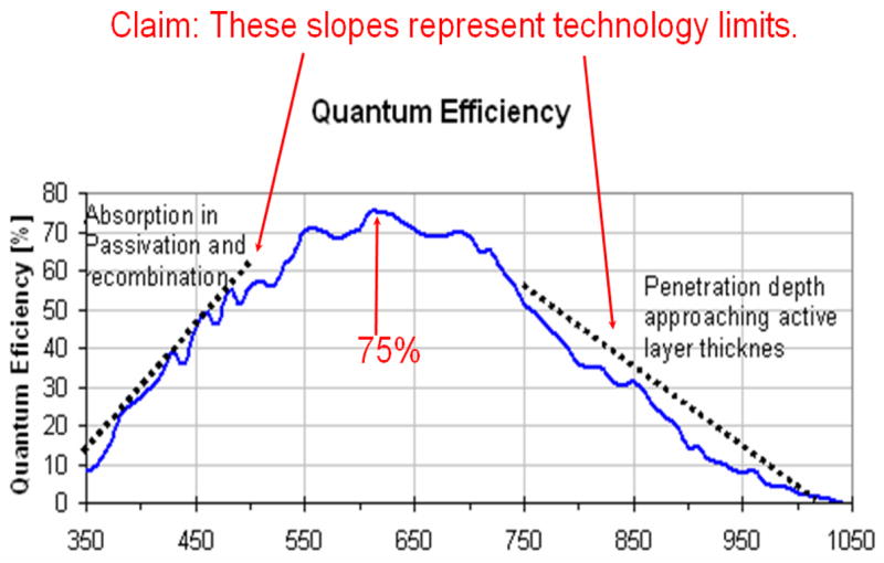
CMOS quantum Efficiency
From Sze Chapter 1 [4] we observe that the green light intensity is down to 1/α at 1μm. Therefore the N-well photodiode (with a junction depth of 1.3 μm) in TS18 process is the selection for the photo detector in this Full Field Digital Mammography imager.
2.5 Radiation effect on silicon photo detector
From reference [5], the total x-ray dose effect on a silicon CMOS device consists of the threshold voltage variation and the significant increase of the drain current. The threshold shifting of the irradiated device can be compensated with a reversed diode at the input. The leakage current of a device exposed to x-rays is reduced by the close geometry layout of the N-device. In addition, we also replace the N-device at the pixel RESET and column selection by the P-device. The implementation of the pixel can be found in Figure 3. Figure 4 illustrates the radiation hardening layout. We employed the guideline from NASA for radiation hardened layout for all the logic of the row decoder because these electronics are exposed to an x-ray radiation environment.
Figure 4.

Pixel implementation
2.6 Silicon photodiode simulation model
A simulation model for the photodiode is proposed by Swe and Yeo in [6]. The noise components of the photodiode model are omitted for simplicity. The model is shown in Figure 5 below.
Figure 5.

Radiation hardening layout
And the frame readout speed simulation circuit is in Figure 7.
Figure 7.

Readout frame rate optimization Simulation schematic
2.7 Analog signal processing path
There are two design approaches which can be used for the analog signal readout path. They are: Correlated Double Sampling (CDS) and Delta Sampling (DS). We use the DS architecture for the FFDM image sensor. The block diagram of the Full Field Digital Mammography IC is shown in the Figure 8.
Figure 8.

Full Field Digital Mammography Imager block Diagram
2.8 Process Stitching
Many semiconductor-processing foundries have a maximum lithographic size that they may use to form a chip. A common limit, for example, is 20*20 mm2. Making a chip larger than that maximum size may be carried out using stitching. There are three popular stitching methods: 1) the filled reticle, 2) the abutted reticle and the 3) sub-field stitching. In the filled reticle, each IC is as large as the limit of the lithographic size. In this case, the IC will have the dimensions of 2cm × 2cm. The maximum number of die per 200 mm wafer is 58. The abutted reticle stitching method can be used to generate a large IC which has a layout occupying 04 adjacent reticles. The maximum number of die per 200 mm (e.g., 8″) wafer for this stitching method is 12. For larger die, we have to use the sub-field stitching method. This technique can be used to fabricate from 01 die per 200 mm wafer to 04 dies per wafer. Figure 9 from [7] illustrates this concept.
Fig. 9.

Large Scientific Image Sensor Stitching
The typical issues for sub-Field stitching are: 1) Misalignments between stitch module which results in shorts between VDD and VSS or power bus shorted to the pixel signal bus, and 2) Stringent shorts between metals. The preliminary analysis indicates that the foundry does not have any misalignment problems.
2.9 Readout rms Noise
In order to match the Bioptics Small Field Digital Mammography imager, we need to keep the FFDM sensor readout is at 250 electron rms or less. The noise performance model is shown in Figure 10 [8].
Fig. 10.

FFDM Analog Noise Model
The only known method for reduction of the reset noise (kTC noise) is the use of a soft RESET architecture. Since the FFDM pixel design is the same as in the Bioptics Small Field Digital Mammography image sensor, the current pixel reset in FFDM sensor is hard reset. However, we put in the effort to keep the rest of the analog signal processing path at the same level or less than the SFDM simulated noise.
2.10 FFDM Contrast-Detail Performance
The CDMAM (Contrast-Detail Mammography) phantom, which is shown in Figure 11, is manufactured by Nuclear Associates [9] and was specifically developed to test mammographic equipment. It consists of an aluminum base with gold discs of varying thicknesses (0.03–2.00 μm) and with diameters of 0.06–2.00μm. The gold discs are arranged in a matrix of 16 rows and 16 columns, which are at 45° to the phantom edges. Along the rows and columns the diameter and the thickness are kept constant, respectively. Since most combinations of disc thickness and diameter can be found in the array, this phantom can be quite easily used to determine the limits of an x-ray imaging system in terms of detail size and contrast. In every grid cell there are two gold discs: one is located at the center of the cell and one is located in one of the four corners. The random distribution of the second, eccentric disc ensures that “learning effects” of the observer who is evaluating the test images are minimized.
Fig. 11.
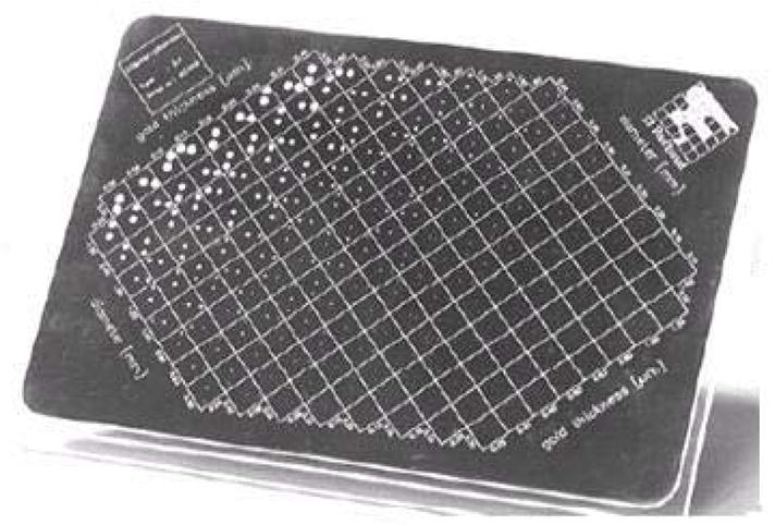
CDMAM Phantom
Supplementary Material
Figure 6.

Photodiode spice simulation Model
Acknowledgments
Our thanks to Tower Semiconductor for design review and layout verification support. We also appreciated the University of Arizona ECE Department for all of the additional technical review, and advice during the design of FFDM image sensor.
References
- 1.http://www.lot-oriel.com
- 2.www.pi4.physik.uni-erlangen.de/Giersch/ROSI/
- 3.www.pi4.physik.uni-erlangen.de/Giersch/RAVAR
- 4.Sze Simon M. Physics of Semiconductor Devices. 1985. [Google Scholar]
- 5.http://rd49.web.cern.ch/RD49/MaterialRadCourse/FAnghinolfi.pdf
- 6.Swe TN, Yeo KS. An Accurate Photodiode Model for DC and High Frequency SPICE Circuit Simulation. Tech Proc. of the 2001 International Conference on Modelling and Simulation of Microsystems; Hilton Head Island, South Carolina. March 2001; pp. 362–365. [Google Scholar]
- 7.http://www.noao.edu/meetings/lsst/kozlowski.pdf
- 8.after R.I. Hornsey, University of Waterloo, CA
- 9.http://www.inovision.com/NuclearAssociates
- 10.http://www.cs.berkeley.edu/~lazzaro/class/guestlec/cs250_sp07_cmos_imager.pdf
Associated Data
This section collects any data citations, data availability statements, or supplementary materials included in this article.