Abstract
This paper investigates the structural characteristics of templated synthetic anti-ferromagnetic (SAF) magnetic nanoparticles fabricated on two different release layers. When copper was used as the latter, the layered structure of the SAFs was found to be disrupted with wavy multi-layers due to the formation of copper grains from the release layer. By introducing oxygen into the copper release layer before the deposition of the film, the topography of the oxidized-copper grains was effectively controlled. This led to the fabrication of SAF nanoparticles with flat multi-layers.
Keywords: Transmission Electron Microscopy, Magnetic nanoparticles, Magnetic Thin Films
1. Introduction
Magnetic nanoparticles (MNPs) are potential candidates for biomedical applications such as cell labeling, bio-magnetic sensing and separation. This involves functionalizing the MNPs with a species that selectively binds to the target analyte, bio-chemically immobilizing the magnetically-labeled analytes on a magnetic sensor chip and then separating them from unwanted entities by rinsing the sensor chip. The amount of analytes present can be determined from the change in sensor output signal when an external magnetic field is applied [1]. Accurate quantification requires that the MNPs be uniform in shape, size, composition and free from clustering. For good signal-to-noise ratio, they should possess high magnetic moments at low applied magnetic fields and no remanence when no magnetic field is applied.
Synthetic Anti-ferromagnetic (SAF) nanoparticles [2,3,4,5] represent a new paradigm wherein ferromagnetic components are used to produce monodisperse, low remanence and high moment nanoparticles. Each SAF is composed of two Co90Fe10 layers separated by a non-magnetic ruthenium (Ru) spacer layer. Tantalum (Ta) is used as a protective capping layer to passivate and stabilize the nanoparticles when they are suspended in water. Unlike conventional MNPs that are produced via chemical synthesis routes, the SAFs are fabricated on a silicon substrate using nanoimprint lithography (NIL) and direct deposition of multilayer films. The process, as described in [5], involves vacuum coating the Si wafer with a 50 nm chemically etchable release layer of copper (Cu) (indicated as “release layer”) and then depositing a Ta buffer layer of approximately 3 nm to minimize oxidation of the Cu during subsequent resist bakes. Following that, thermal nanoimprinting was performed on the substrate to produce 100 nm-diameter pillars. Metallic multilayers that make up the SAF nanoparticle structure and topped with a thick Ta protective capping layer were sequentially deposited in an ion beam deposition system.
Releasing the SAFs from the substrate into aqueous medium (de-ionized water) involved an additional step of ion milling through the thin Ta buffer layer to expose the Cu release layer and then etching the latter with ammonia-cupric sulfate solution. The released particles were collected by five cycles of centrifugation and solvent exchange, and finally re-suspended in de-ionized water.
This paper is an extension of our work in [6], where we reported on the formation of SAF nanoparticles with wavy layers. The preliminary findings suggested this to be due to the formation of grains in the Cu release layer and their propagation into the SAF structure. Here, we describe how unevenness in copper grain topography can be mediated by introducing oxygen to the release layer prior to film deposition.
2. Sample Preparation and Experiments
SAF nanoparticles with structure Sub(Si/Ta40/Cu500/Ta30)/Ta40/Ru20/Co90Fe1060/Ru25/Co90Fe1060/Ru20/Ta170 and Sub(Si/Ta40/CuOx500/Ta30/)Ta40/Ru20/Co90Fe1060/Ru25/Co90Fe1060/Ru20/Ta170 (numbers denote nominal film thicknesses in angstroms) were fabricated using the same method as described in [5]. The nominal thickness of both specimens was kept constant and was monitored using a quartz microbalance during the ion beam deposition process. The only variable was the introduction of 2.5×10⁻⁶ Torr oxygen during Cu release layer deposition using a variable leak valve for the second specimen (hereafter we refer to them as samples on “copper release layer” and “oxidized copper release layer” respectively).
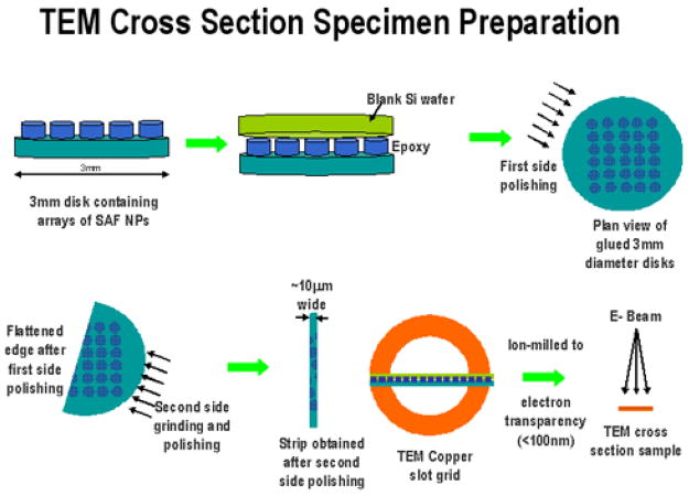
To investigate the structure of the SAF nanoparticles, transmission electron microscopy (TEM) cross section specimens were prepared (Figure 1). First, 3 mm diameter disks comprising templated SAF arrays are bound onto a blank Si substrate of equivalent dimensions with G1 resin and hardener mixed in the ratio 10:1 (Gatan Inc., Pleasanton, CA). Next, the interface was mechanically thinned down with diamond lapping films of grit sizes 30, 15, 9, 6, 3, 1, 0.5 and 0.1 μm, via standard grinding and polishing tools (T-tool, Precision TEM Inc., Santa Clara, CA). At approximately 10 μm thickness, the specimen was removed from the T-tool glass fixture by immersing it in acetone. It was then glued to a TEM Cu slot grid, and further etched to electron transparency using a Gatan 691 Precision Ion Polishing (PIPS) System.
Figure 1.
TEM cross section specimen preparation for substrate-bounded SAF nanoparticles.
All specimens were studied using a Philips CM20-FEG TEM fitted with an Energy Dispersive X-ray Spectrometer operating at 200 kV at the Stanford Nanocharacterization Laboratory (SNL).
3. Results and Discussion
3.1 TEM analyses
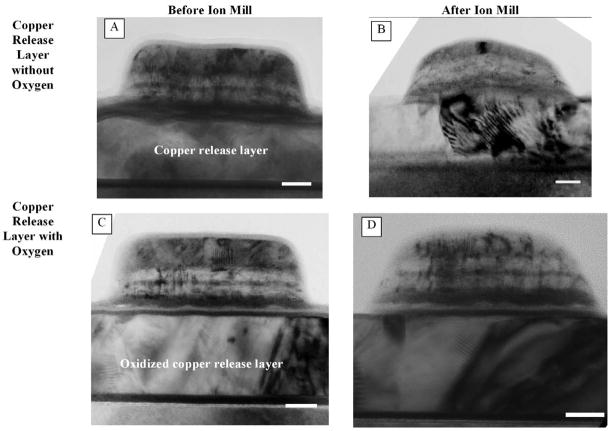
Figures 2A and 2C are low magnification, TEM bright field (BF) images of SAF nanoparticles fabricated on copper and oxidized copper release layers respectively. The multilayer nature of the particles is visible in these images, as is the thick Ta capping layer on the top of the particles. From the TEM images, the structure of the SAFs (excluding substrate) on copper release layer was found to be Ta38/Ru20/Co90Fe1059/Ru26/Co90Fe1060/Ru20/Ta170 (numbers in angstroms) whereas that on oxidized copper release layer was Ta39/Ru21/Co90Fe1059/Ru26/Co90Fe1060/Ru20/Ta170 (numbers in angstroms). Figures 3A and 3B are higher magnification TEM BF images of SAF nanoparticles from the same samples, illustrating the difference in film topography due to the release layers. Particles deposited on copper release layer (Figure 3A) were found to compose of wavy multilayers. The undulation of the layers was due to rippling from the copper release layer. This phenomenon was mediated when oxygen was introduced to the copper before deposition of the SAF structure. Figure 3B shows that nanoparticles fabricated on an oxidized copper layer comprised straighter multilayers.
Figure 2.
TEM bright field images of SAF nanoparticles fabricated on copper release layer (A and B) and oxidized copper release layer (C and D). Figures (B) and (D) illustrate the change in particle shape after the ion milling process prior the release stage. The scale bar represents 20nm.
Figure 3.
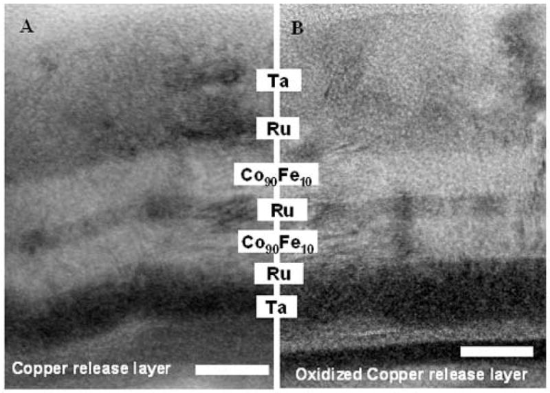
TEM bright field images of SAF structure deposited on (A) copper release layer (no oxygen) and (B) oxidized copper release layer. Wavy inter-layers are observed in (A). The scale bar denotes 10nm.
Releasing the substrate-bound particles into aqueous medium (de-ionized water) involved an additional step of ion milling to remove part of the Ta buffer layer to expose the copper layer for etching. We examined the effects of ion milling on SAF morphology using TEM by cleaving each substrate into two after the initial deposition, retaining one and ion milling the other. This resulted in four variations of TEM samples. Figures 2B and 2D show the low magnification, TEM BF images of the SAF nanoparticles, on copper and oxidized copper respectively, after ion milling. In both images, part of the Ta capping layer had been removed in the ion milling process and the shape of the particle had changed from cylindrical to dome-shaped. The columnar growth of the copper could also be seen in Figure 2B. Alternating Gradient Magnetometry (AGM) measurements indicate that SAF nanoparticles fabricated on both copper (Figure 4A) and oxidized copper (Figure 4B) release layers show a slight decrease in the magnetic moments after the ion milling process. This might be attributed to reduced Ta passivation on the side walls of the nanoparticles after ion milling, leading to some oxidation in the ferromagnetic constituents. However, other magnetic parameters, such as coercivity, magnetic remanence and saturation field, are not affected by ion milling. These results lead us to conclude that ion milling has little compromise on magnetic properties of the SAF nanoparticles.
Figure 4.
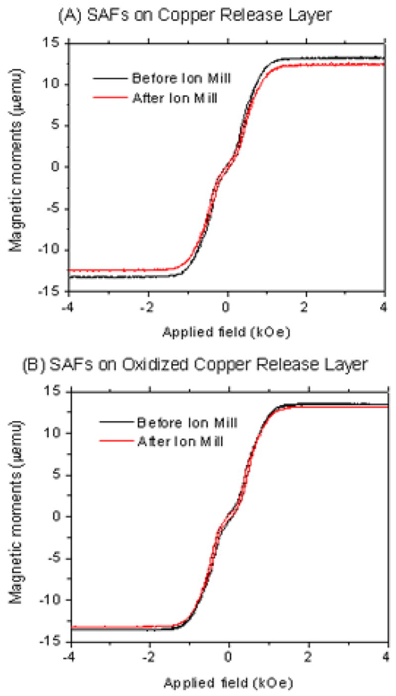
Alternating Gradient Magnetometry (AGM) measurements of SAF nanoparticles fabricated on (A) copper and (B) oxidized copper release layers, before and after ion milling, showing slight decrease in magnetic moments after the ion milling process.
3.2 Surface topography of Cu film using AFM characterization
To gain insight into the surface topography of copper and its possible changes due to oxygen, four specimens comprising films of structure Ta50/Cu500 (numbers denote nominal thicknesses in angstroms) were deposited on unpatterned Si(100) wafers at room temperature in an ion beam sputtering chamber, where oxygen was introduced with a partial pressure of Po2= 0, 1×10⁻⁷, 1×10⁻⁶ and 1×10⁻⁵ Torr respectively. The samples were then characterized using an atomic force microscope (AFM) operating in tapping mode. Figure 5 shows the changes in surface topography due to the introduction of oxygen at various pressures. Without the presence of oxygen, the copper film grew into islands and the amplitude of the surface roughness (Ra) was 9.4 Å. The island growth was suppressed with the introduction of oxygen and Ra was reduced to 3.2 Å at the highest experimental pressure of 1×10⁻⁵ Torr.
Figure 5.
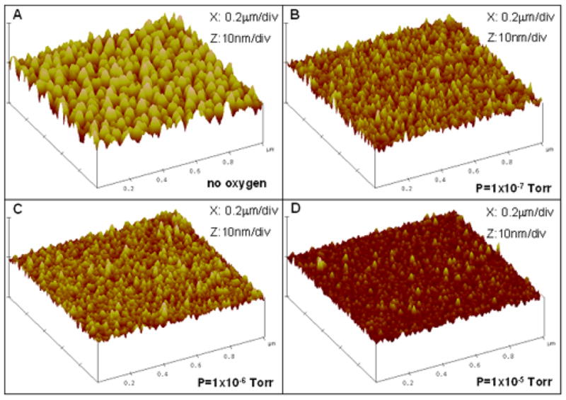
AFM images illustrating the changes in surface topography due to the incorporation of oxygen at various pressures.
3.3 Effect of film topography on magnetic properties
Interlayer roughness is expected to play an important role in the interlayer coupling. Exchange coupling and topographic magnetostatic coupling (also known as Néel “orange peel” coupling) are the two major contributions. The former is oscillatory with the thickness of the spacer layer and the latter is a function of several aspects of the thin-film structure including layer composition, number of multilayer repeats as well as the morphology of the layer interfaces [7]. The effect of interlayer roughness on the interlayer exchange coupling has been studied in Co/Cu giant magnetoresistance spin valves [8,9]. It was found that a decrease in interfacial roughness led to an increase in antiferromagnetic coupling and consequently an improvement in magnetoresistance ratio.
Even though the morphology at the SAF nanoparticle interface has improved with the introduction of oxygen to the release layer, its effects on magnetic properties have been mixed. Our magnetic characterization data (Figure 6) shows slight changes in M-H loops for SAF nanoparticles with different release layers. One of the reasons is that the Ru spacer layer in SAF structure is so thick that interlayer exchange coupling is too weak to be observed. Reducing Ru spacer layer thickness to a certain range (such as < 7Å) is expected to result in stronger antiferromagnetic exchange coupling [10,11], but the saturation field of such SAF nanoparticles is too large to be useful in the applications we are currently interested in.
Figure 6.
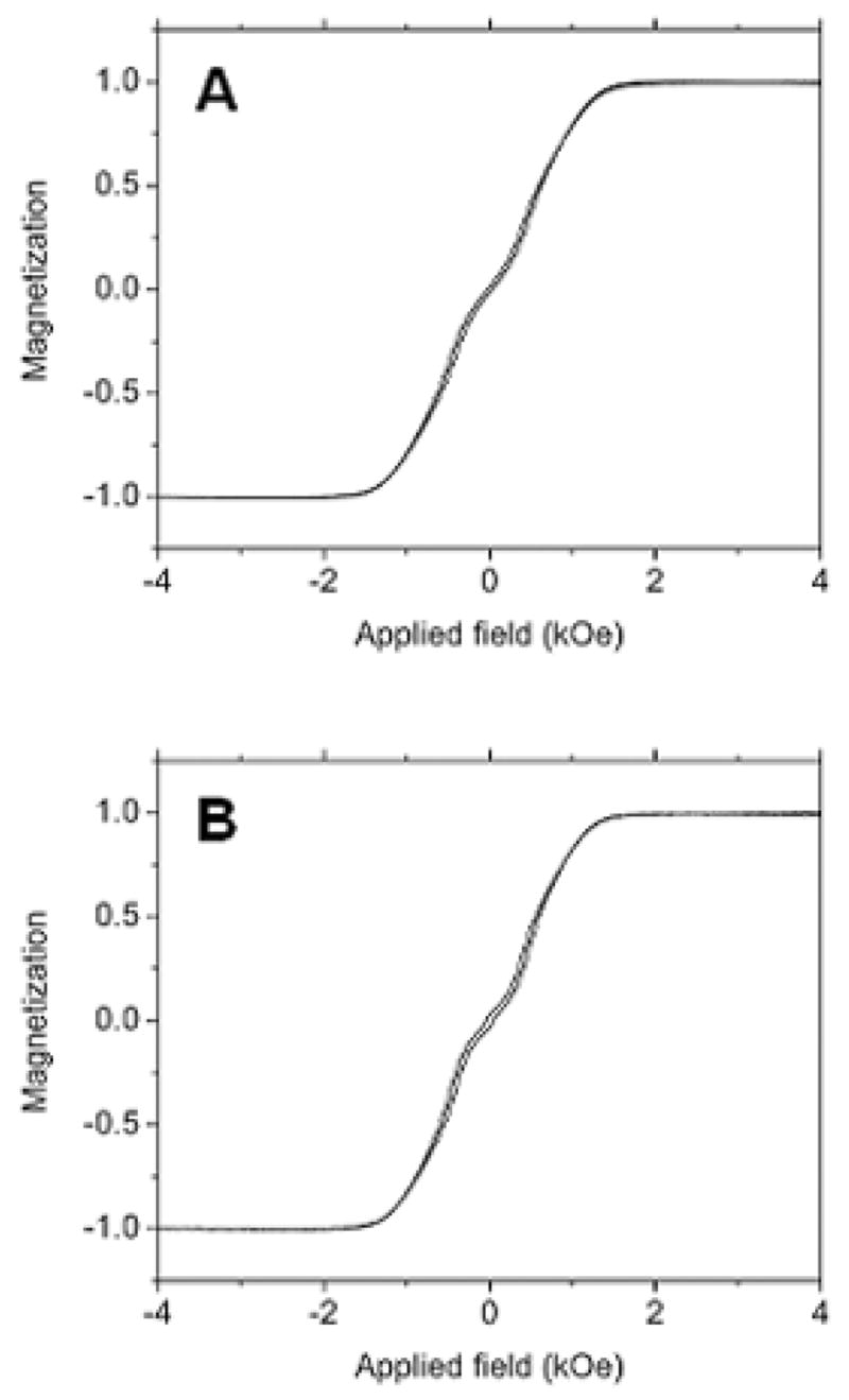
In plane M-H curves of SAF nanoparticles with different release layers characterized by alternating gradient magnetometry (AGM). (a) SAF with 500 Å Cu. (b) SAF with 500 Å oxidized Cu.
4. Conclusions
Structural characterization of SAF nanoparticles fabricated using different release layers was performed by preparation and analyses of Transmission Electron Microscopy (TEM) cross-section specimens from arrays comprising SAF nanoparticles. When copper was used as the release layer, the layered structure of the SAFs was found to be disrupted and wavy multi-layers were observed, due to the formation of copper grains of varying heights from the release layer. When oxygen was introduced into the release layer prior the film deposition process, the topography of the oxidized-copper grains was effectively controlled and consequently, SAF nanoparticles with flatter multi-layers were fabricated. TEM analyses thus resulted in an important improvement in the structural properties of the SAF nanoparticles.
Table 1.
AFM data of average and root-mean-square (RMS) surface roughness of copper as a function of different oxygen pressure.
| Oxygen Pressure (Torr) | Average surface roughness (Å) | Root-Mean-Square (RMS) surface roughness (Å) |
|---|---|---|
| no oxygen | 9.4 | 11.5 |
| 1×10⁻⁷ | 5.2 | 6.5 |
| 1×10⁻⁶ | 4.0 | 5.1 |
| 1×10⁻⁵ | 3.2 | 4.2 |
Acknowledgments
This work is supported by the Center for Cancer Nanotechnology Excellence Focused on Therapy Response (CCNE-TR) grant (NIH U54) and the Nanyang Technological University (Singapore) Overseas Scholarship (ALK).
Footnotes
Publisher's Disclaimer: This is a PDF file of an unedited manuscript that has been accepted for publication. As a service to our customers we are providing this early version of the manuscript. The manuscript will undergo copyediting, typesetting, and review of the resulting proof before it is published in its final citable form. Please note that during the production process errors may be discovered which could affect the content, and all legal disclaimers that apply to the journal pertain.
References
- 1.Häfeli U, Schütt W, Teller J, Zborowski M. Scientific and Clinical Applications of Magnetic Carriers. Plenum Press; New York: 1999. [DOI] [PMC free article] [PubMed] [Google Scholar]
- 2.Wang SX, Wilson RJ, Hu W. Patent Application No. 60/760,221 US Provisional. 2006
- 3.Wilson RJ. US Patent 5932097 1999 2002
- 4.Koh AL, Hu W, Wilson RJ, Wang SX, Sinclair R. Microsc Microanal. 2007;13(Suppl 2):66CD. [Google Scholar]
- 5.Hu W, Wilson RJ, Koh AL, Fu A, Faranesh AZ, Earhart CM, Osterfeld SJ, Han SJ, Xu L, Guccione S, Sinclair R, Wang SX. Adv Mat. 2008 doi: 10.1002/adma.(200703077). in press. [DOI] [Google Scholar]
- 6.Koh AL, Hu W, Wilson RJ, Wang SX, Sinclair R. Structural and Magnetic Characterization of Synthetic Anti-ferromagnetic (SAF) nanoparticles. doi: 10.1016/j.ultramic.2008.03.012. in preparation. [DOI] [PMC free article] [PubMed] [Google Scholar]
- 7.Li K, Wu Y, Qiu J, Han G, Guo Z, Xie H, Chong T. Appl Phys Lett. 2001;79:3663. [Google Scholar]
- 8.Egelhoff WF, Jr, Chen PJ, Powell CJ, Stiles MD, McMichael RD, Judy JH, Takano K, Berkowitz AE. J Appl Phys. 1997;82:6142. [Google Scholar]
- 9.Miura S, Tsunoda M, Takahashi M. J Appl Phys. 2001;89:6308. [Google Scholar]
- 10.Parkin SSP, More N, Roche KP. Phys Rev Lett. 1990;64:2304. doi: 10.1103/PhysRevLett.64.2304. [DOI] [PubMed] [Google Scholar]
- 11.Parkin SSP. Phys Rev Lett. 1991;67:3598. doi: 10.1103/PhysRevLett.67.3598. [DOI] [PubMed] [Google Scholar]


