

Abstract
This article describes a high-performance transconductance amplifier specifically designed for electrotactile (electrocutaneous) stimulation. It enables voltages up to ±600 V to be produced at the output which will allow the psychophysiological performance associated with stimulation of the fingertip using various stimulation waveforms to be studied more thoroughly. The design has a transconductance of up to 20 mA/V, an 8.8-MΩ output resistance, and can provide output currents up to ±20 mA. A complete schematic diagram is presented along with a discussion of theory of operation and safety issues as well as performance and derating plots from the implemented design.
Keywords: Current control, electrocutaneous, electrotactile, transconductance amplifier
I. Introduction
ELECTROTACTILE stimulation passes a localized electric current through the skin in order to stimulate underlying touch nerves and thus evoke tactile sensations. This process can be used in sensory substitution—receiving via one sense information that is normally received by another sense. In the case of electrotactile stimulation, it is often vision or hearing information that is received by touch. The principles and applications of electrotactile stimulation and sensory substitution have been summarized in several review articles [1-4, 5 (Chapter 7), 6, 7 (pp. 12:42−48), 8, 9].
The impedance of the skin can be quite variable due to environmental conditions, sweat gland activity, skin type, etc., and also decreases significantly with stimulation current [10-16]. Therefore, the stimulation current, rather than the voltage, is usually controlled. The most challenging skin location for electrotactile stimulation is the fingertip, for which the resistive component of the impedance (which also has a capacitive component) has been reported as high as 320 kΩ [17]; we have observed even higher values in our lab. It is therefore important that the proposed circuit have a very high output impedance (ideally infinity) so that the delivered current is insensitive to variations in load impedance. High voltage capability (compliance, up to 700 V, more typically 150−300 V) is also required, as is a slew rate consistent with the particular application or experiment; we set 50 V/μs as a design goal. These requirements (explored in more detail in [17]) are difficult to meet using extant commercial instrumentation, published circuit designs and semiconductor devices.
Our high-voltage bipolar transconductance amplifier (HVB-TA) is based on an earlier design we have used in our lab for 15 years [18], which had a maximal voltage capability of ±120 V, or with a modified asymmetric power supply, up to 240 V positive or negative pulses, but not both. It had an output resistance of 2 MΩ, adequate for electrotactile stimulation on hairy skin but not for glabrous fingertip skin, which is much thicker and has a much higher impedance. Modifications to this circuit include use of stacked darlington transistor pairs to achieve higher voltage capability using low-power semiconductors1 and the addition of an additional feedback loop to achieve a higher output resistance.
The only other transconductance amplifier design we are aware of that approaches these requirements was described by Poletto [17]. That design used high-voltage operational amplifiers arranged in a Howland current pump configuration to achieve voltage-to-current conversion. The chosen semiconductor devices (Apex Microtechnology PA85A) have a maximal rail-rail power supply voltage of 450 V and output swing of approximately 400 V peak-peak, or ± 200 V for bipolar pulses. Achieving higher potentials (± 400 V bipolar, reconfigurable for higher-potential asymmetric pulses) requires a bridge configuration, necessitating either floating the load or the entire amplifier circuit. The former option is not desirable for safety and performance reasons. If coaxial stimulation electrodes are used, the typically large return electrode, tied to one side of the bridge, will cause the average body potential of a human subject to achieve one-half of the total stimulation potential, causing a hazard should the subject touch an external conductor and causing a significant displacement current to flow otherwise. Conversely, floating the amplifier necessitates a complex isolation scheme for both the power supplies and the input circuitry. The latter was achieved using a combination of analog and digital optical isolators to preserve both pulse level and sharp edge transitions. This scheme, however, limits the use of arbitrary wave shapes and necessitates separate analog and digital inputs.
Poletto's design has excellent feedback-based current control, fast rise times (< 1 μs), and is capable of delivering indefinitely long current pulses undistorted. However, several disadvantages prompted us to develop an alternative circuit: (1) The output potential swing is too low for full-range (±700 V) biphasic pulses on the fingertip, (2) The input waveform is limited and requires separate analog and digital inputs, (3) The operational amplifiers are expensive (> US$200) and power-hungry (> 20 mA quiescent current, yielding 9 W power dissipation with ±225 V rails), and (4) the circuit topology is very sensitive to component selection and physical layout to prevent instability and failure of the operational amplifiers. Electrotactile stimulator designs by other investigators [e.g. 19, 20-22], being designed for specific applications, do not have specifications adequate for our research.
The design presented here is capable of producing +600/−800 V, ±20 mA, bipolar current-controlled waveforms given the appropriate input voltage waveform. With ±800 V rails, the quiescent current (power) of each amplifier channel is approximately 1.0 mA (1.6 W). Each amplifier channel incorporates quite a few discrete components (28 transistors, 4 analog integrated circuits, and several dozen passive components) but even with predominantly through-hole mounting the printed circuit board size is only 10.7 × 14.3 cm. Up to 16 amplifer channels can fit in a standard 6 in (15.2 cm) high, 19 in (48.3 cm) wide equipment rack. Each amplifier incorporates provisions for adjusting gain, output resistance, and compensation for stray capacitance in the electrode wiring. We include here a complete schematic diagram, theory of operation, and detailed performance specifications measured for various resistive and cutaneous electrode loads. Table 1 shows a list of key specifications (see performance section for further details).
Table 1.
Specifications. Maximum ratings are based on component manufacturer's published ratings. Performance specifications are measured; see details in main text and Figures 6-9.
| Specification | Notes | Value | Units | |
|---|---|---|---|---|
| INPUT | Transconductance | Knob and jumper adjustable | 0−20 | mA/V |
| Minimum Input Voltage | To produce up to ±20 mA at output | ±1 | V | |
| Maximum Input Voltage | To prevent damage | ±40 | V | |
| Input Resistance | 10 | kΩ | ||
| OUTPUT | Output charge limit | For user safety | 160 | μC |
| Maximum Current | Nominal; see derating curves | ± 20 | mA | |
| Output Resistance | Without Ro compensation feedback | 717 | kΩ | |
| With Ro compensation feedback | 8.8 | MΩ | ||
| Rise Time | For 100 kΩ load | < 10 | μs | |
| Slew rate | For 100 kΩ load | 45 | V/μs | |
| Maximum Voltage | Asymmetric and depends on load and rail voltages; | +800, | V | |
| see derating curves | −600 | V | ||
| Overshoot | Step transition into 100 kΩ load | <5 | % | |
| Settling Time | Step into 100 kΩ load, settle to 2% final value | 22 | μs | |
| Load grounding | One side must be grounded | --- | --- | |
| Linearity | Percent deviation from delivered current | ≤ 8 | % | |
| Percent deviation from full scale output | ≤ 1 | % | ||
| Pulse width | Maximum | 250 | μs | |
| Duty cycle | Pulse width * rate | 10 | % | |
| Power supply current (No input signal) | LV | 25 | mA | |
| HV | 0.4 | mA | ||
| Power supply current (100Hz, 100μs, 20mA bipolar signal) | LV | 30 | mA | |
| HV | 1.7 | mA | ||
II. THEORY OF OPERATION
By definition, a transconductance amplifier takes a voltage as an input and produces a directly proportional current at the output. An ideal transconductance amplifier has an infinite output resistance so that the output current is independent of load impedance, and the output current waveform would have an identical shape as the input voltage waveform. A real TA has a finite output resistance, reducing the accuracy of current control, and there is furthermore noticeable rounding of the current waveform due to the effect of stray capacitance. To compensate for these imperfections, feedback control loops have been implemented and will be discussed below, along with the general operation of the TA itself. Note that to simplify circuit analysis among the transistors, the operation of the positive half of the circuit will be described and it can be assumed that the negative half will behave similarly.
Four figures provide both a complete schematic drawing as well as illustrate the key feedback loops in the circuit. Figure 1 shows the essential TA circuit, and is called the Base Amplifier. Figure 2 shows the Complete Amplifier, including the additional feedback loops compensating for stray capacitance and output conductance. Figure 3 conceptually shows the four feedback loops. Figure 4 shows the power supply.
Fig. 1.
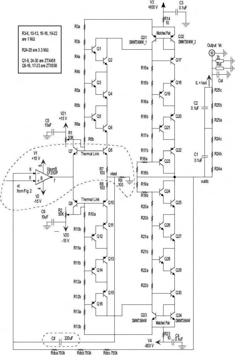
Base Amplifier. This is the main voltage-to-current converter circuit. A positive input voltage vt is converted into a current signal in Q8 by the components encircled by dashed lines (negative inputs are handled by Q10; see main text). The matched transistors Q31 and Q32 reflect the current in the transistor stack above Q8 back down the transistor stack below Q32. Therefore, the output current iL is close to vt/R9. The darlington-configured transistor stacks divide voltage evenly to achieve high voltage amplifier capability with readily-available semiconductor devices.
Fig. 2.
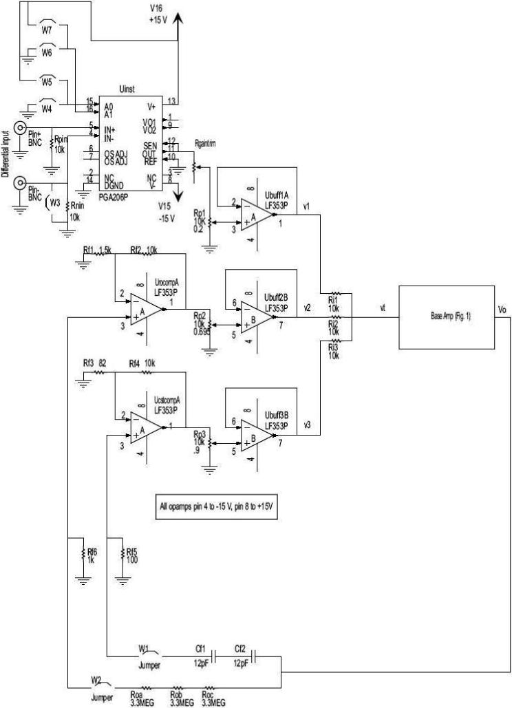
Complete Amplifier. This circuit shows how the Base Amplifier is supplemented by feedback loops that compensate for stray capacitance and conductance in the Base Amplifier and output cabling. The instrumentation amplifier PGA206P is by Texas Instruments.
Fig. 3.

Feedback Loop Summary. The overall HVB-TA has four feedback loops. The current control loop and dc stabilization loop are integral parts of the Base Amplifier (Fig. 1) and essential to its operation. Two additional loops external to the Base Amplifier compensate for stray capacitance and conductance in the output circuit and related cabling.
Fig. 4.
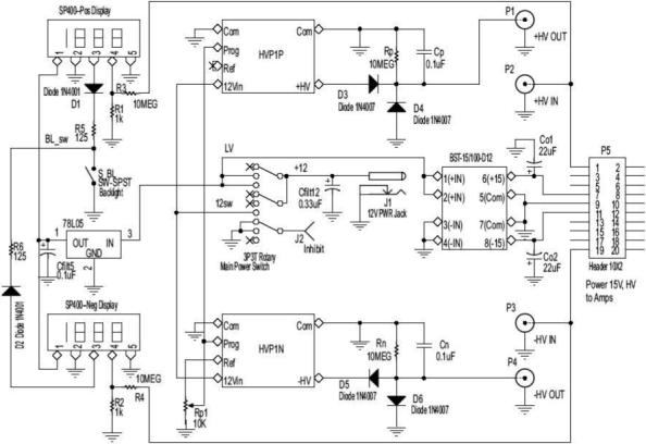
Power Supply. Power supply modules HVP1P and HVP1N are by Pico Electronics (Pelham, New York), power supply module BST-15/100-D12 is by Datel/Murata (Mansfield, Massachusetts), and digital displays SP400 are by Lascar Electronics (Erie, Pennsylvania).
Current Control Loop
In the Base Amplifier (Figure 1), the input voltage vt is converted into a current by the loop formed by UsumB, Q8, R9 and Cif (bounded by dashed line). Q7 is diode-wired and thermally-bonded to Q8 to minimize thermal drift in the quiescent operating current, which is adjustable by varying R1. The loop is also represented in Figure 3 by the block containing Cif. This current feedback loop causes the pulse voltage at vtest to be nearly equal to the input voltage, vt. It can be assumed that either the positive or negative half of the circuit will be turned on at an instance in time, but not both. Therefore, the current through R9 will either take the path through R7 or R8, but not both2. Using
| (1) |
and
| (2) |
this input voltage is converted into a current. (β > 90 for the current range of interest, 1−20 mA). This current conversion and the current mirror to be described next operate similarly to our earlier design [18].
Current Mirror
The Wilson current mirror formed by Q31, Q32 and Q17 reflects Q31's collector current, iC31, to Q17's collector current, iC17. Note that iC31 is a function of iC8, and the output current, iout, is a function of iC17. This is important because it allows the load to be grounded and therefore multiple electrodes can share a common return path. The Wilson current mirror has three characteristics that suit it well for this application. First, it has better matching of input and output current than other methods. Second, it is less dependent on transistor β variations. Third, it does not require the β of Q17 to be matched to that of Q31 and Q32 and Q17 can therefore be implemented by a high-voltage transistor [18]. Assuming all the transistors in the circuit have a similar current gain, and Q31 and Q32 are a matched pair, Q17's collector current, iC17, can be represented as a function of iC31 by:
| (3) |
Also, if Equation (2) is applied to transistors Q2, Q4, Q6, Q18, Q20 and Q22, then
| (4) |
and
| (5) |
Static Transfer Function
The static transfer function of this part of the circuit can be formed by combining (1)−(5):
| (6) |
Since R9 = 100 Ω and β ≈ 100, this is about 9.33 mA/V. When measured, gm was approximately 9.6 mA/V. Notice that in (6), gm is relatively independent of load resistance and power supply voltage. Also, β may vary with temperature, but a 10% change in β will result in only a 0.6% change in gm.
DC stabilization loop
The current feedback loop is capacitively-coupled by Cif and hence will not transfer any dc voltage. However, Rdc (i.e. Rdca+Rdcb+Rdcc) provides negative-feedback dc from the output, as shown in Figure 3. The circuit's large voltage gain forces the dc component of outdc to track the small dc component seen at vt, for any conceivable electrotactile stimulation waveform. The resulting net dc load current is therefore minimized.
Output ac Coupling
If one of the output transistors were to fail, a dangerous dc current could flow from the high-voltage supply to the subject. To prevent this, capacitors C1 and C2 couple the electrode to output transistors Q22 and Q25. Any residual dc drop that may develop across these capacitors is equally distributed by R24−25.
Bias Point Stabilization
The quiescent current through Q8 and Q10 is maintained at about 0.4 mA by R1 and R7. It can be adjusted through R1, which is implemented as a variable resistor. Q7 is diode-wired and thermally linked to Q8 to reduce bias point variations due to temperature changes. A similar quiescent current can be assumed to travel down the output stack of transistors (Q17-Q23). Also, a small current will go through R3-R6 and R15-R18. The quiescent current delivered to the “positive” input stack of transistors (Q1-Q6) and resistors (R3-R6) is therefore about
| (7) |
or approximately 0.4 + 0.1 mA for V3 = 800 V, which means that the total quiescent current measured through R14 is double that, or about 1.0 mA.
As mentioned earlier, the Base Amplifer has a nonzero output admittance that reduces the accuracy of current control and distorts the current waveform. The Complete Amplifier in Figure 2 shows the addition of two feedback loops that compensate for these effects, as well as a differential input configuration for noise reduction.
Output Stray Capacitance Compensation Loop
A stray capacitance, Cst, ranging from 40 to 200 pF, may develop at different points in the circuit, output cable or electrode array. This essentially creates a low-pass filter at the output and distorts the output current waveform at the electrode load, ZL. To compensate for this, Cf = Cf1Cf2/(Cf1 + Cf2) provides a differentiated positive-feedback path from the TA output to its input. In the equation
| (8) |
| (9) |
where the gstVo(s) term is a function of the conductance due to the circuit having a non-infinite output resistance and the sCstVo(s) term is a result of the stray capacitance, the stray capacitance compensation signal component is averaged into Vt(s). This component is labeled as v3 in the circuit schematic and it is a function of Vo(s) by
| (10) |
Note that {Rp3} refers to the potentiometer's wiper's fractional position from ground (i.e. 0−1). Equation (9) then becomes:
| (11) |
| (12) |
| (13) |
Since sCf is very small relative to Rf5, can be simplified to approximately sCfRf5, and so
| (14) |
Therefore if , the effect of stray capacitance, Cst, on the output current waveform will nearly disappear, independent of the load impedance, ZL. Note that with {Rp3} = 1, up to 229 pF of stray capacitance may be compensated for3.
Output Resistance Compensation Loop
The ideal current source will have an infinite output resistance, Rout, so that the same current will be always be delivered regardless of the load. The actual Rout of the circuit without compensation is about 717 kΩ, which is too low4. As was mentioned previously, the variable that represents this non-ideality is gst, which can be seen in Eq. (14). In order to compensate for this, a small positive-feedback voltage is brought back to the input at v2 from the output by
| (15) |
where Ro = Roa+Rob+Roc. Rp2 is adjusted to attenuate this feedback voltage and acquire the highest Rout possible without causing the circuit to become unstable for an open-circuit load. The measured Rout is then about 8.8 MΩ, which is acceptable. Combining (14) and (15), the mathematics behind this compensation loop is clarified in the load current equation by:
| (16) |
| (17) |
Therefore, if , the term containing gst is eliminated.
Gain Adjustment
Potentiometer Rp1 is implemented as a front panel knob which allows for adjustment of the gain. Jumpers W4-W7 have been included to easily adjust the gain of the instrumentation amplifier to 1, 2, 4 or 8 V/V. Also, Rgaintrim was included in this design so that the gains of each channel can be calibrated to be equal for a certain gain knob setting.
Differential Input
Finally, the instrumentation amplifier, Uinst, provides a differential input and thus most common-mode noise in the input cabling is rejected. Therefore, the input component that is summed to form vt is a function of (vin+ - vin-). Note that due to the very high input impedance of Uinst the inputs will pick up a lot of noise if left floating. Hence Rpin and Rnin ensure that the inputs will not float.
Overall Transfer Function
V1(s) in (17) is equal to (Vin+(s) – Vin−(s)){Rp1}, and noting that Vo(s) = IL(s)ZL(s), the circuit's entire static transfer function can be written as:
| (18) |
Note that the denominator of this equation is of the form:
| (19) |
where Kggst is the term due to the finite output resistance, K1{Rp2} is the adjustable term to compensate for that, KcCst is the stray capacitance resulting term and K2{Rp3} is the corresponding adjustable compensation term. If the compensation terms are adjusted correctly, it is evident that the majority of this denominator will cancel out and the equation simplifies to the form of an ideal TA, with terms dependant on the load impedance eliminated:
| (20) |
Feedback Paths
Figure 3 summarizes the feedback loops of the circuit in a more conceptual manner. The current-control loop is formed by the Cif block. Likewise, the dc-stabilization loop is formed by the Rdc block. These two negative feedback paths implement voltage-to-current conversion and maintain dc stability. Two positive feedback paths compensate for stray capacitance (Cf and KCst blocks) and output circuit conductance (Ro and KRo blocks).
Semiconductor Selection
With maximal ±800 V power supply voltages, Q2, Q4, Q6, Q8, Q10, Q11, Q13, Q15, Q17, Q18, Q20, Q22, Q25, Q27, Q29 and Q30 need to withstand 400 V, yet they must operate at low currents of 0.1 to 50 mA. Although the specified VCE breakdown voltage of 400 V is adequate, the ones used were individually tested to withstand at least 500 V to reduce the possibility of failure if the maximal rail voltages are used. The Darlington pair configuration is used with the majority of these for its high gain characteristic. Matched pair transistors Q31−32, and Q33−34, were selected for their collector current rating as well as flat β and matched characteristics from 0.1 to 50 mA. The only ones found to meet our needs are only available in a surface mount package. Lastly, as previously mentioned, Q7 and Q9 are glued to Q8 and Q10, respectively, in order to provide a thermal link.
Power Supplies
The circuit uses both low-voltage (±15 V) and high-voltage (±800 V) for operation as shown in Figure 4. In order to minimize output transients, proper power sequencing must be observed. To implement this, a three-position power switch (off, low-voltage, high-voltage) is used. When switched from “off” to “low-voltage”, only the ± 15 V supply is turned on. This activates the feedback paths and amplifier, thus giving the circuit time to stabilize at its dc operating point. When switched to “high-voltage”, the ±800 V supply is applied to the now stable circuit. If the power supplies were sequenced in the opposite order or even at the same time, the high voltage would be applied to an essentially unstable circuit, and the output is momentarily unpredictable.
To increase usability, two high-voltage power supply schemes are available. One, implemented by miniature DC-DC converters, is typically intended to be used with up to three channels due to current limitations.5 The second high-voltage supply scheme uses external high-voltage power supplies.
III. SAFETY FEATURES
There are a number of safety features incorporated into the design to prevent the subject from electrical injury, which are explained below:
Redundancy
The TA circuit schematic shows that three faults (e.g. shorted C1, shorted C2 and a shorted output transistor, assuming other transistors would then fail in a chain reaction) are required to connect the subject to the high voltage and pass the full power supply current to them. If using the internal power supplies, the maximum output current from each is 5 mA. External power supplies may also have the ability to limit their output current. Note that these three failures are a worst-case scenario and extremely unlikely. For less than three failures, less than 0.1 mA DC will be applied to the output.
Charge-Limiting Output Coupling
The output coupling capacitors are of low enough value to ensure that the charge flowing into any single electrode under any condition will not exceed 160 μC. This is less than 290 μC, the Underwriters Laboratories limit for capacitive discharges for a 0.1 μF capacitance [5].6
Power Supply
A 120 VAC-12 VDC converter which brings the power to the circuit is a medical-grade separate external unit. Therefore, dangerous AC voltages are kept apart from the actual instrument.
IV. PERFORMANCE
We built and tested the HVB-TA design, which has been in use in our lab for over one year for research completed and in progress [23, 24, 16]. Fig. 5 shows a photograph of one complete amplifier channel (including the Base Amplifier in Fig. 1 and the feedback loops and input circuitry in Fig. 2). The power supply is on a separate module, not shown. The circuit was implemented using mostly through-hole components on a 2-layer printed circuit board. Surface-mount techniques and a more efficient layout could be used to achieve a more compact design.
Fig. 5.
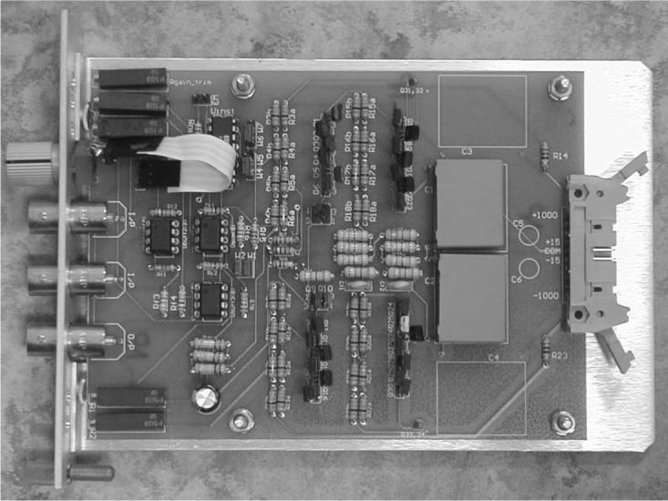
Photograph of one complete amplifier channel. The printed circuit board has dimensions of 10.7 × 14.3 cm and is mounted on an equipment rack module (13.3 × 16.9 × 2.5 cm). At left are the front panel gain knob and BNC input and output connectors (not included in module dimensions). The trim potentiometers on the top and bottom left edge of the board are the gain trim, bias current, and resistance and capacitance compensation adjustments. The connector on the right side of the board receives power from a separate power supply module (13.3 × 16.9 × 5.0 cm) mounted in the same rack.
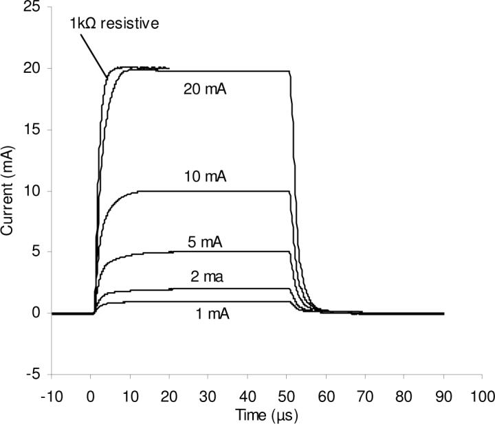
Figures 6 and 7 show the actual current waveform delivered to various resistive and fingertip electrode loads in response to a square input voltage (vt) pulse with a risetime of approx. 2 μs. As expected, higher-valued resistive loads showed larger current risetimes, consistent with greater RC time constants, C representing primarily the uncompensated stray capacitance in the output circuit and cabling. Electrode loads, which have significant capacitive components [16], showed faster rise times than purely resistive loads of the same resistance value. Figure 8 shows the electrode voltage for the same stimulation conditions used for Fig. 7. The faster rise time at higher currents is attributable to a reduction of both resistive and capacitive components of the electrode-skin load at higher currents [25, 16].
Fig. 6.
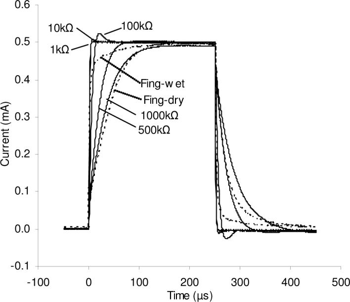
Dynamic response for a nominal 0.5-mA, 250-μs current pulse delivered to resistive (1−1000 kΩ) and typical fingertip electrode (dotted line) loads. This low (and subthreshold) current enables time response to be compared across a wide range of load resistances without exceeding the HVB-TA output voltage limit. The stainless steel fingertip electrode had a coaxial structure with a 0.9-mm-diameter center electrode and an annular surround with inner and outer diameters of 4.8 and 6.4 mm, respectively. The Fing-dry data were recorded within one minute after the electrode was placed onto a dry patch of fingertip skin. Fing-wet (hydrated) conditions were recorded 5 min after an electrode was placed on fingertip skin, allowing sweat to build up under the electrode and reduce skin resistance. Current was measured using a 300-MHz digital oscilloscope and a 100-Ω current-sampling resistor in the return current path; for the electrode, this was the surround. The HVB-TA R0 compensation loop was adjusted to minimize the difference in asymptotic maximal current between 1-kΩ and 500-kΩ resistive loads, i.e., to minimize the effect of load resistance. This is equivalent to maximizing the output resistance of the circuit. The C0 compensation loop was adjusted for best dynamic response (i.e., fastest rise time without overshoot) for a 500-kΩ resistive load. C0 compensation is slightly dependent on load resistance, as evidenced by the slight overshoot with 1 and 10 kΩ resistive loads.
Fig. 7.
Dynamic response for 50-μs current pulses delivered to a well-hydrated fingertip electrode (see Fig. 6 legend) with nominal currents ranging 1−20 mA (sub-threshold to painful). The top trace shows the response for a 1-kΩ resistive load (showing only the rising phase for clarity; the falling phase is similar).
Fig. 8.
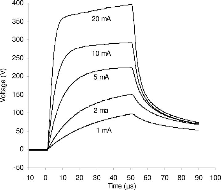
Electrode voltage resulting from the 50-μs, 1−20 mA current pulses shown in Fig. 7 (well-hydrated fingertip electrode). A X100 high voltage probe was used with the oscilloscope to record these data.
Figure 9 shows the measured maximal voltage and current capability of the HVB-TA for various resistive loads similar to typical fingertip resistances. (Significant portions of these curves would result in painful stimulation if real electrodes were used.) Although these derating curves reflect primarily the fundamental voltage and current limits of the circuit, certain asymmetries not observed in simulation indicate the possibility of improvement by better physical layout for reduction of stray capacitance. See legends for Figs. 6-9, for further details on the performance of the HVB-TA as actually built.
Fig. 9.
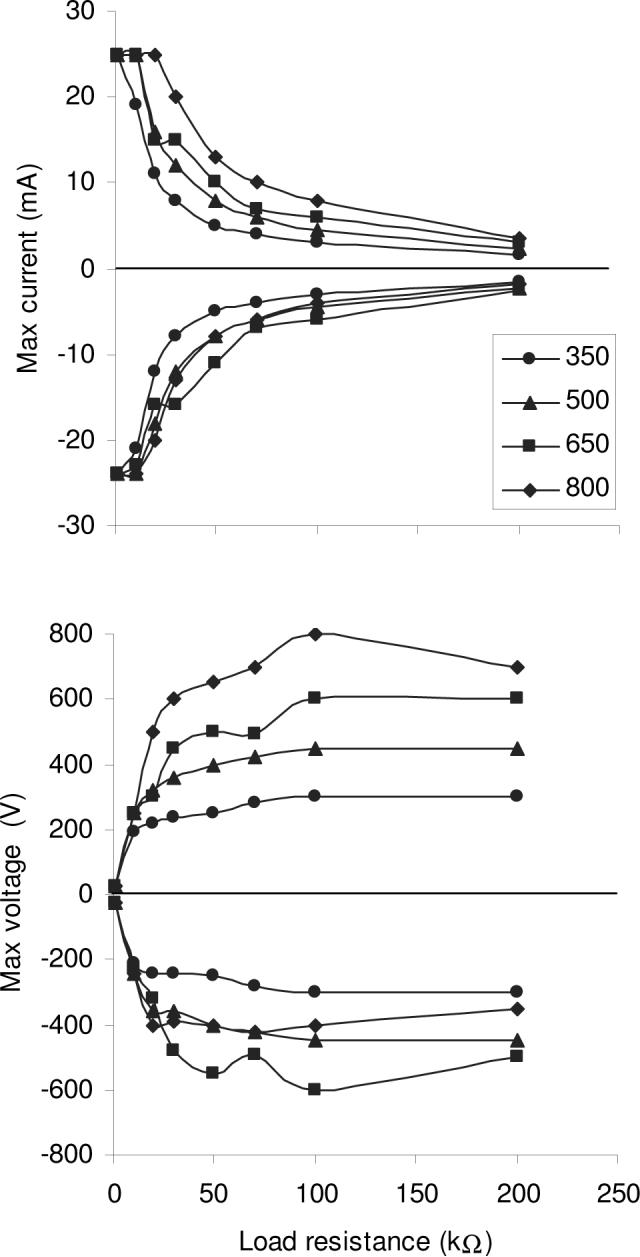
Maximal undistorted output current and voltage measured for resistive loads of 1, 10, 20, 30, 50, 70, 100, and 200 k Ω . These values varied only minimally over pulse widths 20−250 μs and pulse rates 10−100 Hz. The output was primarily current-limited for low load resistance and voltage-limited for high load resistance. The legend shows the symmetrical ±HV rail voltages for the output circuit. The somewhat lower output limits for negative pulses and high rail voltages was not observed in simulation. We assume that this effect is due to stray capacitance in the assembled circuit.
V. CONCLUSIONS
The design presented above is a stable and reliable transconductance amplifier to be used in an electrotactile stimulation system for the fingertip. It is an improvement to past designs because of its stability and ability to reliably produce bipolar current pulses up to ±600 V. Feedback loops have been incorporated to optimize the output for typical stimulation waveforms. These features will allow electrotactile stimulation of the fingertip to be studied more thoroughly in future experiments.
Biography

Matthew A. Schaning received the B.S. degree in biomedical engineering from Marquette University, Milwaukee, WI in 2004, and the M.S. degree in biomedical engineering from the University of Wisconsin, Madison, in 2005. He studied biomedical instrumentation and sensory substitution. Since 2005, he has been an Engineer in the Research and Development Department, Energy-Based Devices, Covidien, Boulder, CO. His current research interests include tumor ablation and instrumentation.

Kurt A. Kaczmarek (M’86–SM’05) received the B.S. degree in electrical engineering from the University of Illinois, Urbana, in 1982 and the M.S. and Ph.D. degrees, both in electrical engineering, from the University of Wisconsin- Madison, in 1984 and 1991, respectively. From 1984 to 1986, he was a Senior Engineer with Baxter International, Deerfield, IL. He is currently a Senior Scientist at the University of Wisconsin- Madison, where, since 1992, he has studied the mechanisms and perception of electrical stimulation of touch. His interests include tactile displays, sensory rehabilitation and augmentation, teleoperation, and neurorehabilitation.
Footnotes
We chose low-power semiconductors because they have better amplification characteristics than high-power devices in the current region of interest, 0.5−20 mA. Low-power devices are available with breakdown potential of only 400 V, necessitating the voltage division scheme.
Actually, each circuit half (e.g. R7 or R8) has a dc quiescent current of 0.3−0.5 mA to prevent crossover distortion. Currents in this analysis represent deviations from this quiescent operating point. R7 and R8 serve to stabilize the dc operating point but do not contribute to voltage-to-current conversion.
Under-compensation, i.e. {Rp3} too small, results in slow dynamic response; overcompensation, i.e. {Rp3} too large, results in ringing or oscillation. The maximal stray capacitance compensation was tested by setting {Rp3} = 1 and adding capacitance across a 500-kΩ load until ringing disappeared, approx. 600 pF. This exceeds the theoretical value of 229 pF, probably due to stray circuit board capacitance in parallel with the tiny feedback loop capacitor Cf (6 pF).
Rout may be calculated by first measuring the output current amplitude for a certain input voltage pulse with a purely resistive load, and the output current amplitude for the same input voltage using a different resistive load. Using current division equations, .
The specified HV converters deliver 5 mA, while each amplifier channel consumes 1.7 mA from the HV rails for a 20-mA, bipolar, 1% duty cycle output. This is a high current and duty cycle for electrotactile stimulation. The amplifier channels may operate at even higher duty cycles (see Table 1), but this requires more power and therefore the three-channel limit is reduced.
Our design is not UL tested or rated and is intended to be used by knowledgeable personnel for experimental purposes. The 160-μC fault rating assumes that one output capacitor is shorted, and that the other capacitor is pre-charged to 800 V by maximal conduction in one output polarity transistor stack, and that the opposite polarity stack subsequently shorts (an extremely unlikely scenario). The 0.1-uF capacitor then reverses polarity, requiring 160 μC for the resulting 1600-V voltage swing.
Contributor Information
Matthew A. Schaning, University of Wisconsin, Madison, WI 53706 USA. He now works for Covidien, Boulder, CO 80301 USA (phone: 262−490−2482; e-mail: mschaning@gmail.com).
Kurt A. Kaczmarek, Department of Orthopedics and Rehabilitation Medicine and the Department of Biomedical Engineering, University of Wisconsin, Madison, WI 53706 USA (e-mail: k.a.kaczmarek@ieee.org)..
REFERENCES
- 1.Gibson RH. Electrical stimulation of pain and touch. In: Kenshalo DR, editor. The Skin Senses. Charles C. Thomas; Springfield, IL: 1968. pp. 223–261. [Google Scholar]
- 2.Kaczmarek KA, Webster JG, Bach-y-Rita P, Tompkins WJ. IEEE Trans. Biomed. Eng. Vol. 38. 1991. Electrotactile and vibrotactile displays for sensory substitution systems; pp. 1–16. [DOI] [PubMed] [Google Scholar]
- 3.Kaczmarek KA, Bach-y-Rita P. Tactile displays. In: Barfield W, Furness T, editors. Virtual Environments and Advanced Interface Design. Oxford University Press; New York: 1995. pp. 349–414. [Google Scholar]
- 4.Kaczmarek KA. Sensory augmentation and substitution. In: Bronzino JD, editor. CRC Handbook of Biomedical Engineering. CRC Press; Boca Raton, FL: 2000. pp. 143.1–143.10. [Google Scholar]
- 5.Reilly JP. Applied Bioelectricity. Springer; New York: 1998. [Google Scholar]
- 6.Rollman GB. Electrocutaneous stimulation. In: Geldard FA, editor. Proc. Conf. Cutan. Comm. Sys. Dev.; Psychonomic Society. 1973.pp. 38–51. [Google Scholar]
- 7.Sherrick CE, Cholewiak RW. Cutaneous sensitivity. In: Boff KR, Kaufman L, Thomas JP, editors. Handbook of Perception and Human Performance: vol 1: Sensory Processes and Perception. Wiley; New York: 1986. pp. 12.1–12.58. [Google Scholar]
- 8.Szeto AYJ, Saunders FA. Electrocutaneous stimulation for sensory communication in rehabilitation engineering. IEEE Trans. Biomed. Eng. 1982;BME-29:300–308. [PubMed] [Google Scholar]
- 9.Szeto AYJ, Riso RR. Sensory feedback using electrical stimulation of the tactile sense. In: Smith RV, Leslie JH Jr., editors. Rehabilitation Engineering. CRC Press; Boca Raton, FL: 1990. pp. 29–78. [Google Scholar]
- 10.Boxtel A. v. Skin resistance during square-wave electrical pulses of 1 to 10 mA. Med. Biol. Eng. Comput. 1977;15:679–687. doi: 10.1007/BF02457927. [DOI] [PubMed] [Google Scholar]
- 11.Grimnes S. Skin impedance and electro-osmosis in the human epidermis. Med. Biol. Eng. Comput. 1983;21:739–749. doi: 10.1007/BF02464037. [DOI] [PubMed] [Google Scholar]
- 12.Kaczmarek KA, Webster JG. Voltage–current characteristics of the electrotactile skin–electrode interface. In: Seattle WA, Kim Y, Spelman FA, editors. Proc. Annu. Int. Conf. IEEE Eng. Med. Biol. Soc.; IEEE. 1989.pp. 1526–1527. [Google Scholar]
- 13.Kajimoto H, Kawakami N, Maeda T, Tachi S. Electrocutaneous display with receptor selective stimulation (II) - Skin impedance based control. Proc. Virtu. Reality Soc. Japan Fifth Annu. Conf..2000. [Google Scholar]
- 14.Lykken DT. Square-wave analysis of skin impedance. Psychophysiol. 1971;7:262–275. doi: 10.1111/j.1469-8986.1970.tb02232.x. [DOI] [PubMed] [Google Scholar]
- 15.Panescu D, Webster JG, Stratbucker RA. A nonlinear electrical-thermal model of the skin. IEEE Trans. Biomed. Eng. 1994;41:672–680. doi: 10.1109/10.301734. [DOI] [PubMed] [Google Scholar]
- 16.Sreenivasan A. M.S. Thesis. Univ. of Wisconsin-Madison; 2007. Variation of Electrical Characteristic of the Electrotactile Electrode-Skin Interface with Position and Current Thresholds. [Google Scholar]
- 17.Poletto CJ, Van Doren CL. A high voltage, constant current stimulator for electrocutaneous stimulation through small electrodes. IEEE Trans. Biomed. Eng. 1999;46:929–936. doi: 10.1109/10.775402. [DOI] [PubMed] [Google Scholar]
- 18.Kaczmarek KA, Kramer KM, Webster JG, Radwin RG. A 16-channel 8-parameter waveform electrotactile stimulation system. IEEE Trans. Biomed. Eng. 1991;38:933–943. doi: 10.1109/10.88439. [DOI] [PubMed] [Google Scholar]
- 19.Chu H. M.S. Thesis. University of Wisconsin-Madison; 1987. Tactile feedback system for space suit glove: electrotactile stimulation. [Google Scholar]
- 20.Onesti RJ, Tompkins WJ, Webster JG, Wertsch JJ. Design of a portable electrotactile stimulator for sensory substitution applications. In: Kim Y, Spelman FA, editors. Proc. Annu. Int. Conf. IEEE Eng. Med. Biol. Soc.; IEEE. 1989.pp. 1439–1440. [Google Scholar]
- 21.Takahashi H, Kajimoto H, Kawakami N, Tachi S. Electrotactile display with localized high-speed switching. Int. Conf. Artificial Reality Telexistence (ICAT); Tokyo, Virtual Reality Society of Japan. 2002. [Google Scholar]
- 22.Kajimoto H. Ph.D. Thesis. University of Tokyo; 2004. The Electric Tactual Sense Display (Japanese) [Google Scholar]
- 23.Jayaraman A, Kaczmarek KA, Tyler ME, Okpara UO. Effect of localized ambient humidity on electrotactile skin resistance. Proc. Northeast BMES 2007 Conf.; Stony Brook, New York, IEEE. 2007. [Google Scholar]
- 24.Okpara UO, Kaczmarek KA, Tyler ME. Two perceptual dimensions result from manipulating electrotactile current and frequency. Proc. Northeast BMES 2007 Conf.; Stony Brook, New York, IEEE. 2007. [Google Scholar]
- 25.Kaczmarek KA, Webster JG. Voltage-current characteristics of the electrotactile skin-electrode interface. In: Seattle WA, Kim Y, Spelman FA, editors. Proc. Annu. Int. Conf. IEEE Eng. Med. Biol. Soc.; IEEE. 1989.pp. 1526–1527. [Google Scholar]