Abstract
Control of the fundamental absorption edge of a quantum dot with an applied electric field has been limited by the breakdown fields of the solid-state material surrounding the dot. However, much larger fields can be applied at the interface of two immiscible electrolytic solutions (ITIES) in an electrochemical cell. These electric fields also localize the quantum dots at the ITIES. Our analysis shows that semiconductor nanocrystals localized at the ITIES should have electric-field-tunable optical properties across much of the visible spectrum. The transparency of the liquids in such cells indicates that this configuration would be well suited for electrically tunable optical filters with wide-angle acceptance.
Keywords: immiscible electrolytic solutions, optical absorption
Quantum dots have tunable electronic, optical and magnetic properties depending on nanocrystal diameter (1). Control of the fundamental absorption edge with an applied electric field, through the Stark effect (2), has been limited by the electrical breakdown of the material surrounding the dot, typically occurring at ≈100–500 kV/cm because of impact ionization. Fields greatly in excess of those possible in semiconductor materials can be applied at the interface of two immiscible electrolytic solutions (ITIES) in an electrochemical cell (3, 4), and can be sustained (at least transiently) within a semiconductor nanoparticle (5). Furthermore, nanoparticles can be reversibly localized at this interface through the application of an electric field, whereupon they self-assemble in a two-dimensional layer. Semiconductor nanocrystals localized at ITIES should have optical properties tunable across much of the visible spectrum, corresponding to at least a 560–620-nm wavelength for CdSe/ZnS dots (green to red). The transparency of the liquids in such cells indicates that this configuration would be well suited for a previously uncharacterized class of self-assembled electrically tunable optical filters.
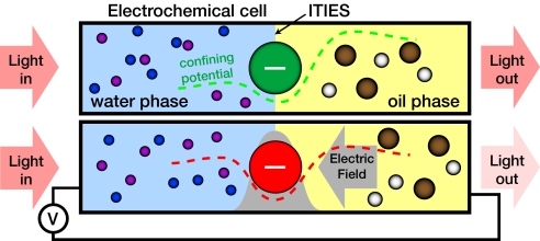
ITIES occurs between two immiscible liquids (water and an organic fluid) mixed with two salts, one of hydrophilic ions residing in the aqueous phase and one of hydrophobic ions in the organic phase (3–6). Under the influence of an electric field, two “back-to-back” electrical double layers are formed on the two sides of the interface (Fig. 1). For typical organic solvents, e.g., 1,2 dicloroethane or nitrobenzene, the interface supports a voltage up to 0.8 V without the ionic current flow across the interface (3, 4). The potential drop is localized at the interface within the two double layers, i.e., within a 1-nm region, depending on salt concentrations, thus corresponding to fields up to 0.8 V/nm. This spatial dimension is compatible with semiconductor quantum dots, whose diameters can be as small as 2 nm with 5% size variability. For CdSe/ZnS dots, this diameter corresponds to a 490-nm wavelength of emission, in the blue region of the visible spectrum. Thus, ITIES provides a defect-free region for the localization of nanoparticles (7).
Fig. 1.
Schematic view of ITIES with negatively charged nanoparticle adsorbed at the interface, with and without applied electric field. Nanoparticle color indicates peak optical absorption, which is changed by the electric field. Positive and negative ions are shown as small spheres: violet and blue (in water) and brown and white (in oil). The gray arrow indicates the electric field direction, and the gray filled region indicates the field strength. The electric field pushes the negatively charged nanoparticle toward the oil phase, and a dashed line sketches the total potential that confines the nanoparticles to the interface (8).
To avoid agglomeration of nanoparticles, they are protected by ligands, attached to the particles by thiol groups, with hydrophilic acidic terminal groups that can dissociate in aqueous phase at normal pH. This results in a net charge of the coated particles that is, however, much smaller than the number of ligands, because of Coulomb repulsion between ionized groups. Solvation of charged nanoparticles drives them toward the aqueous phase, whereas the properly applied electric field drives them toward the organic phase, generating an electrochemical potential minimum (deepened by surface tension and the polarizability of the nanoparticle) at a region of large electric field (8).
In contrast to larger uncharged particles that spontaneously adsorb at liquid–liquid interfaces to reduce interfacial energy, small charged nanoparticles tend to stay in the water phase in the absence of an electric field. The contributions to the confining potential for nanoparticles at the interface between two ITIES include competitive wetting, the solvation energy for the charged nanoparticles, the polarizability in an external field, line tension, and the potential contribution from the applied electric field. Calculations demonstrate (8) that the electric fields possible at the ITIES can provide a sufficiently deep potential well to localize the nanoparticles at the interface. Variation of the electric potential allows reversible control of the well depth and therefore the coverage of the interface by nanoparticles. Variation of the concentration of nanoparticles at the interface with an applied electric field will alter the “opacity of the interface.” This effect may provide tunability further than that permitted by the voltage-tunable color selectivity coming from the Stark effect.
The response time of the optical extinction coefficient will be determined by the longer of two times: the response time of the electrical double layers, τm, and the response time of the quantum dots in the modified electric field, τd. A change of the potential distribution at the interface, resulting in a new value of the electric field, requires recharging the “back-to-back” double layers at the interface. This will take the so-called migration time, which is estimated as τm = LLD/Di, where L is the macroscopic dimension of the cell, LD is the Debye screening length or its equivalent in a double layer nonlinearly responding to the overall voltage drop (9, 10), and Di is the diffusion coefficient of the ions. Note the limiting counterpart will be the migration of ions through the oil, primarily because of the higher oil viscosity relative to water. Considering a microfluidic (thin) cell e.g. L = 100 μm, LD = 1 nm, and Di = 10–6 cm2/s, we get τm = 10–3 s.
If the surface concentration of the nanoparticles changes significantly with potential, there is another relaxation time to be taken into account. This time will depend on the (i) average concentration of nanoparticles and (ii) size and charge of the nanoparticles, which influences their Stokes radii, and thus their diffusion coefficient. The corresponding time can be estimated as τd = l2/Dp, where l = (4πcp/3)−1/3 is the average distance between nanoparticles (cp is their number concentration), and Dp is the nanoparticle diffusion constant. Take, e.g. l = 1,000 nm and Dp = 10–7 cm2/s, to get the relaxation time τd = 10–1 s. This slow response time is not relevant when the particle stays at the interface for the full range of electric fields. In that case the field variation will lead to only a minor adjustment of the nanoparticles at the interface, related to transport distances on the order of 0.1–0.3 nm (8), and thus one can expect τd on the order of 10–9 s.
A Stark shift in the energies of both electrons and holes confined to nanoparticles occurs under the influence of an external electric field. At high concentrations of electrolyte (molar or even decimolar), the capacitance of the interfacial monolayer of semiconductor nanoparticles is substantially lower than the capacitances of the double layers in the aqueous and organic phases. As a result, the dominant part of the applied electric potential drops across the layer of nanoparticles, providing an unprecedented possibility to tune their optical properties. The approximately linear potential extending through the dot permits carriers to shift nearer to one side of the dot and, in the process, lower their energy. Note, however, that the larger the nanoparticles the lower the electric field will be for a given potential drop across the interface.
In spherical nanoparticles, the shift in energy for a carrier is due to the electric-field-induced mixing between the lowest-order S state and the lowest-order P state with quantization axis parallel to the applied electric field. For a uniform sphere of radius R with a hard wall boundary condition at its surface, the electronic wave function of the S- and P-states are the normalized spherical Bessel functions A0·j0(ksr) and A1·j1(kpr); ks and kp are the smallest positive numbers such that j0(ksR) = j1(kpR) = 0. The electric-field-induced mixing energy between these two states is the matrix element of the electric field component of the Hamiltonian, eEr, between these two states, and corresponds to one-sixth of the potential energy drop across the nanoparticles, qV/6. The Stark shift will then be
 |
where ΔEe (ΔEh) is the energy splitting between the two lowest conduction electron (valence hole) states. If ΔEe and ΔEh are both smaller than qV/6, corresponding to the case of large nanoparticles, then degenerate perturbation theory yields a Stark shift for the absorption peak of qV/3. If not, such as occurs for small nanoparticles, then nondegenerate perturbation theory yields a Stark shift of
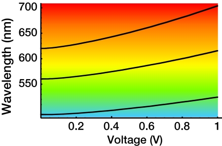
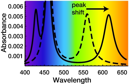
Plots of the peak energy of the lowest-energy absorption feature as a function of electric field are shown in Fig. 2 for three sizes of CdSe/ZnS dots. Such quantum dots as CdSe/ZnS, having a zero-field 560-nm peak lowest-energy absorption line, lie in an intermediate regime where the shift is given by qV/6 ±(qV/6)2/ΔEe = 210 meV. This shift from 560- to 620-nm peak absorption for a 1 V potential, as shown in Fig. 3, corresponds to a change from green to red. This shift is twice as large as the typical room-temperature line width of 30 nm for a quantum dot size distribution of 5%, strongly indicating that this color change survives at room temperature and would have practical importance.
Fig. 2.
Calculated peak wavelength of the low-energy optical absorption as a function of voltage for three sizes of quantum dots. The three curves correspond to zero-field absorption peaks of 490, 560, and 620 nm.
Fig. 3.
Calculated optical absorbance spectrum for a CdSe/ZnS quantum dot with a peak absorption at 560 nm for zero field (dashed line). In the ITIES region an applied voltage of 1 V shifts the peak to 620 nm (solid line).
As mentioned, for the most well studied and robust ITIES, the current flow across the interface becomes significant at 0.8 V; but we also show results for 1 V as a challenge for ITIES. Note that shifts larger than the room-temperature line width can still be achieved for an applied potential as low as 0.5 V for the larger dot (620-nm zero-field absorption peak) shown in Fig. 3, so even with the current well studied ITIES the effect should be remarkable at room temperature.
Nanocrystals of different shape do not have substantially different Stark shifts. The key quantity remains the potential energy drop across the nanoparticles. For example, one-dimensional nanorods with long axes oriented parallel to the applied electric field have calculated Stark shifts that are equal (within 10%) to the Stark shifts for spherical nanocrystals with the same potential energy drop. Thus one may try experiments with different shapes to achieve the largest potential drops across the quantum dots, their most stable localization, and maximal coverage of the interface.
We calculate, according to the method of ref. 11, the optical absorbance of a two-dimensional layer of nanoparticles, assuming a transition from the highest-energy S-state of the valence electrons to the lowest-energy S-state of the conduction electrons. The optical line width is assumed to be 100 meV. The electric field shifts the lowest-energy S-state down in energy and the P-state interacting with it up in energy. The other two P-states do not shift in the applied electric field. Thus, the second-highest-energy absorption feature for the quantum dots, as shown in Fig. 3, does not shift with applied electric field. The characteristics of the absorption will be the higher-energy feature that is independent of field and then a lower-energy feature that shifts substantially with applied electric field, yielding the field-tunable optical filtering properties. The room-temperature extinction coefficient of a dense monolayer of quantum dots, corresponding to a surface density of 1017 m2, would be 0.5% for a single pass (Fig. 3).
Because the formation of this monolayer at an ITIES can be created over cm2 of area, it is straightforward to construct multipass geometries to bring the extinction coefficient near to unity (≈1,000 passes for >99% absorption). For a multipass filter to be feasible, the constituent liquids must have low light absorption in the visible. Distilled water transmits visible light for meters without substantial optical losses. Some oils popular in ITIES studies, such as 1,2-dichloroethane, are similarly transparent in the visible. In a typical ITIES cell, the thickness of each liquid layer is ≈1 cm, although miniaturization to a 1-mm thickness is straightforward (and desirable for a compact optical element). Substantial additional reduction in thickness, such as is common in microfluidic cells, is feasible in principle and does not hinder the operation of this type of filter. Antireflection coatings for the input and output windows will also be required, and can be made >99% transmissive.
Generation of 107 V/cm stable electric fields in the large-area ITIES provides an example where Stark shifts of the optical absorption are larger than the room-temperature line width of colloidal quantum dots. These fields are also larger than the local fluctuating electric fields in the environment of the quantum dots. Previously observed Stark shifts, caused by smaller electric fields, have not approached the room-temperature line width and have also been susceptible to the local fluctuating fields because of the movement of charges on the ligands (2). Self-assembly of a monolayer of quantum dots at the ITIES opens the door to new types of electric-field-tunable optical filters. Applications may include fast, high-extinction, angle-independent energy filters for time-resolved optical probes of biological systems, including two-photon fluorescence.
Acknowledgments.
This work was supported by Leverhulme Trust Grant F/07058/P, Israel Science Foundation Grant No. 773/05, and a U.S. Army Research Office Multidisciplinary University Research Initiative grant.
Footnotes
The authors declare no conflict of interest.
References
- 1.Alivasatos AP. Semiconductor clusters, nanocrystals, and quantum dots. Science. 1996;271:933–937. [Google Scholar]
- 2.Empedocles SA, Bawendi MG. Quantum-confined stark effect in single CdSe nanocrystallite quantum dots. Science. 1997;278:2114–2117. doi: 10.1126/science.278.5346.2114. [DOI] [PubMed] [Google Scholar]
- 3.Girault HH, Schiffrin DH. In: Electroanalytical Chemistry. Bard AJ, editor. Vol 15. New York: Marcel Dekker; 1989. p. 1. [Google Scholar]
- 4.Girault HH. In: Modern Aspects of Electrochemistry. Bockris JO, et al., editors. Vol 25. New York: Plenum; 1993. p. 1. [Google Scholar]
- 5.Klimov VI, et al. Single-exciton optical gain in semiconductor nanocrystals. Nature. 2007;447:441–446. doi: 10.1038/nature05839. [DOI] [PubMed] [Google Scholar]
- 6.Luo GM, et al. Ion distributions near a liquid–liquid interface. Science. 2006;311:216–218. doi: 10.1126/science.1120392. [DOI] [PubMed] [Google Scholar]
- 7.Su B, Fermin DJ, Abid JP, Eugster N, Girault HH. Adsorption and photoreactivity of CdSe nanoparticles at liquid/liquid interfaces. J Electroanal Chem. 2005;583:241–247. [Google Scholar]
- 8.Flatté ME, Kornyshev AA, Urbakh M. Understanding voltage-induced localization of nanoparticles at a liquid–liquid interface. J Phys Condens Matter. 2008;20 073102. [Google Scholar]
- 9.Kilic MS, Bazant MZ, Ajdari A. Steric effects in the dynamics of electrolytes at large applied voltages. I. Double-layer charging. Phys Rev E. 2004;75 doi: 10.1103/PhysRevE.75.021502. 021502. [DOI] [PubMed] [Google Scholar]
- 10.Monroe CW, Urbakh M, Kornyshev AA. Understanding the anatomy of capacitance at interfaces of immiscible electrolytes. J Electroanal Chem. 2005;582:28–40. [Google Scholar]
- 11.Schmitt-Rink S, Miller DAB, Chemia DS. Theory of the linear and nonlinear optical properties of semiconductor microcrystalites. Phys Rev B. 1987;35:8113–8125. doi: 10.1103/physrevb.35.8113. [DOI] [PubMed] [Google Scholar]


