

Abstract
Optoelectronic tweezers (OET) are a powerful light-based technique for the manipulation of micro- and nanoscopic particles. In addition to an optically patterned dielectrophoresis (DEP) force, other light-induced electrokinetic and thermal effects occur in the OET device. In this paper, we present a comprehensive theoretical and experimental investigation of various fluidic, optical, and electrical effects present during OET operation. These effects include DEP, light-induced ac electroosmosis, electrothermal flow, and buoyancy-driven flow. We present finite-element modeling of these effects to establish the dominant mode for a given set of device parameters and bias conditions. These results are confirmed experimentally and present a comprehensive outline of the operational regimes of the OET device.
Keywords: Index Terms, Dielectrophoresis (DEP), electrothermal (ET) flow, light-induced ac electroosmosis (LACE), optoelectronic tweezers (OET)
I. Introduction
The ability to manipulate micrometer- to nanometer-scale particles in a parallel and dynamic fashion is of prime importance in the fields of cellular biology, micro/nano assembly, and microfluidics. A variety of techniques have been explored to this end including optical tweezers [1], [2] and dielectrophoresis (DEP)-based devices [3], [4]. Optoelectronic tweezers (OET) has proven itself to be a powerful tool in these fields [5]–[9]. By using patterned light to transduce local electric-field gradients, particles experience localized DEP-based forces which enable particle control and movement. One of the major benefits of OET is the ability to perform parallel and dynamic manipulation afforded by the use of patterned light. Additionally, OET requires an optical-power density 100 000× less than that often used with optical tweezers.
Until now, there has not been a comprehensive study of the various physical effects present in the operation of the OET device. Light-induced DEP is but one of these forces and lends itself to only a specific set of bias and device parameters. In addition to DEP, localized light-induced heat gradients and electrical double layers (EDLs) in the fluid can interact with the electric fields present resulting in predictable fluid flow and particle movement. It has already been reported that light-induced ac electroosmosis (LACE) is the dominant effect at low-bias frequencies [10]. It is imperative to understand the underlying physics of these effects so that accurate predictions can be made as to what effect is dominant given a set of bias conditions.
II. Theory and Simulation
The OET device structure and setup are shown in Fig. 1(a). The device consists of a photoconductive layer of hydrogenated amorphous silicon (a-Si:H) on an indium tin oxide (ITO)-coated glass substrate. Liquid containing the particles of interest is sandwiched between this lower device and a top piece of ITO-coated glass. An ac bias is applied between the two ITO layers. In the absence of light, the majority of the voltage drops across the a-Si:H layer. However, upon illumination, the a-Si:H layer’s conductivity increases by many orders of magnitude [Fig. 1(c)] due to the creation of electron–hole pairs.
Fig. 1.

(a) OET structure. Electron–hole pairs generated in the illuminated region increase the conductivity of the a-Si:H, resulting in the majority of the applied voltage dropping across the liquid layer. The light pattern is centered at position zero. (b) Simulated electric-field distribution. (c) Experimental a-Si:H conductivity versus optical-power density. (d) Simulated 10-μm-particle velocity versus distance for an optical power of 1 mW and an illumination spot size of 20 μm at 5 μm above the a-Si:H surface. The dotted region corresponds to points within 18 μm of the beam center which are not valid due to the effects of vertical DEP forces acting on the particle. The bias conditions are 10 Vpp and 100 kHz. The velocity of the particle is parallel to the gradient of the electric field. The light pattern is centered at position zero.
The conductivity measurement was obtained by patterning a-Si:H electrodes on an ITO-coated glass substrate. Aluminum electrodes were then patterned on top of the a-Si:H. A 10-mW 632-nm diode laser is sent through a continuous attenuator to a beam splitter, which splits the beam between a photodetector and a 10× objective that focuses the laser light onto a 50 μm × 50 μm a-Si:H square. A series of voltage sweeps are performed across the a-Si:H electrode for varying laser powers. The current is measured for each of these sweeps, and the conductivity is extracted.
The result of the conductivity increase upon illumination causes the voltage to drop across the liquid layer in the vicinity of the illuminated region causing a localized electric-field gradient to occur.
All subsequent simulations are carried out in a commercially available finite-element method (FEM) package (COMSOL Multiphysics 3.2a).
A. Light-Induced DEP
In the presence of light, a localized electric-field gradient is created in the illuminated region [Fig. 1(b)]. The time-averaged force felt by a spherical particle due to this gradient is defined by [11]
| (1) |
where a is the particle radius, εm is the permittivity of the medium, ERMS is the root-mean-square (rms) electric field, and K* is the Clausius–Mossotti (CM) factor, defined as
| (2) |
where and are equal to the complex permittivity of the particle and medium, respectively, which is equal to ε − jσ/ω, where ε, σ, and ω are the electrical permittivity, conductivity, and frequency, respectively.
Depending on the value of the CM factor, the DEP force can either be repulsive or attractive. For the case of polystyrene beads in slightly conducting medium (~1 mS · m−1), the CM factor is less than zero (−0.5), resulting in repulsion from the electric-field intensity maxima and attraction to electric-field intensity minima. Thus, the particle is repelled from the illuminated region [12].
Using Stokes’ formula, we can calculate the velocity under the influence of the DEP force for a spherical particle according to
| (3) |
where η is the viscosity of the fluid. The direction of the velocity vector is parallel to the induced electric-field gradient. Fig. 1(d) shows the maximum DEP velocity for a 10-μm-diameter polystyrene bead at one particle radius away from the surface of the a-Si:H for a 1-mW laser focused to a 20-μm spot size at 10 Vpp and 100 kHz. Note the dotted portion of Fig. 1(d) at the beam center. Points in this region are not valid simulated velocities. This is because the vertical negative DEP-force component will cause the particle to rise off of the OET substrate near the beam center. This occurs when the vertical DEP component and buoyancy forces balance one another. Our simulations and experiments suggest that this occurs at around 18 μm from the beam center for the bias conditions of Fig. 1(d). It is important to note that the horizontal DEP force drops dramatically as one moves away from the substrate–liquid interface. Once the particle leaves the surface, the particle often slips over the light pattern and results in loss of particle control. Therefore, the DEP-induced velocity is only meaningful for distances from the beam center at which the particle still remains on the OET surface.
For this calculation, a Gaussian distribution in conductivity was used to simulate the effect of the illumination spot. The electric-field-gradient profile, with this conductivity distribution, was then extracted via FEM, and the DEP force and particle velocity calculated. These simulations also assume that the relative permittivity of the medium and particle are 78 and 2.56, respectively. These values remain constant throughout the remainder of this paper. Additionally, all subsequent simulations assume a 10-μm particle diameter and a 1-mS · m−1 liquid conductivity, unless otherwise stated.
The simulated velocities of Fig. 1(d) agree with our experimental observations. By scanning a laser line across the OET surface and determining the fastest scan rate at which the particle is still trapped by DEP, one can determine the maximum DEP-induced velocity. For the bias and device conditions of Fig. 1(d), we find a maximum particle velocity of 105 μm/s. This agrees with the maximum valid simulated velocities in Fig. 1(d).
B. LACE
The application of an electrical potential on an ionic fluid results in the formation of an EDL. If a tangential electric-field component is present in the double-layer region, then ions in the layer will move in response to this field. The velocity of these ions is called the slip velocity and is defined by the Helmholtz–Smoluchowski equation [13]
| (4) |
where ε is the permittivity of the liquid, ζ is the zeta potential (defined as the voltage drop across the EDL), Et is the tangential electric field, and η is the fluid viscosity. This fluid velocity is present at the edge of the EDL and results in an overall fluidic flow.
Traditional electroosmosis uses a dc bias and is often employed in the use of microfluidic pumps [14]. More recently, ac electroosmosis has been observed [15]. Here, the ionic charge at the surface of the double layer switches polarity in response to the applied ac field and results in a steady-state motion of the ions in one direction. Lastly, LACE has been reported using the OET device for nanoparticle trapping [10]. In this scheme, a virtual electrode created by patterned light replaces the need for traditional metal electrodes.
AC electroosmosis and LACE both exhibit frequency dependence. This dependence arises out of the fact that the EDL acts as a capacitor and, therefore, has an intrinsic rolloff frequency. Above this critical frequency, the double layer can no longer sustain a voltage drop across itself, and the zeta potential, along with the slip velocity, approach zero.
In the OET device, the creation of a virtual electrode upon localized illumination results in a tangential electric field which produces a slip velocity. In order to model this effect, an equivalent circuit model, as shown in Fig. 2(a), is used to extract the zeta potential. In this model, the EDL is treated as a simple parallel-plate capacitor in series with resistors accounting for the liquid and a-Si:H layers. The double-layer capacitance varies with the layer’s thickness, which is a function of liquid conductivity. This relationship, described by Gouy–Chapman theory, is governed by the following [16]:
| (5) |
where σm is the liquid conductivity, μm is the bulk ion mobility (8 × 10⁻⁸ m2 · V−1 · s−1 for KCl), z is the valence of the ion (e.g., one for KCl), ε is the charge on an electron, k is the Boltzmann constant, and T is the temperature. Here, we have assumed that σm = εμmn0, where n0 is the bulk ion concentration. Fig. 2(b) shows the dependence of the electrical-double-layer thickness on liquid conductivity. For a 1-mS · m−1 solution, the double-layer thickness is about 25 nm.
Fig. 2.
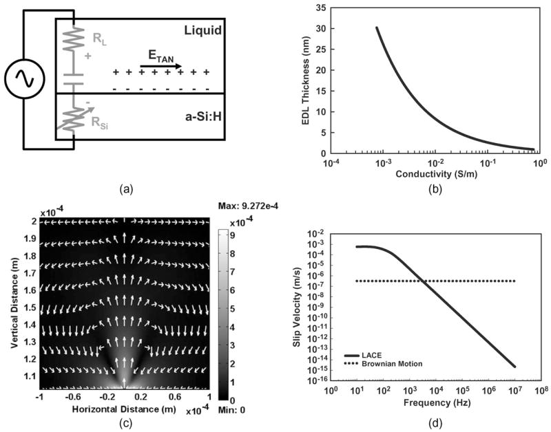
(a) Equivalent circuit schematic of LACE. Ions in the EDL respond to the tangential electric field resulting in a slip velocity. (b) EDL thickness versus conductivity of a KCl solution. (c) Fluid-flow pattern due to LACE in the absence of other forces at 1 kHz and 20 Vpp with an optical-power density of 250 W/cm2. (d) Fluid velocity due to LACE versus frequency at 20 Vpp and 250 W/cm2. A line depicting the distance traveled in 1 s due to Brownian motion for a 10-μm particle is overlaid. Note that, above 1 kHz, the effects of LACE are negligible.
Once the zeta potential is known, the tangential electric field is extracted from simulation, and a slip velocity is calculated. This velocity enters into the Navier–Stokes equation as a boundary condition at the a-Si:H/liquid interface. The resulting fluid-flow pattern is shown in Fig. 2(c) for a bias of 20 Vpp, 1 kHz, 250 W/cm2. Fig. 2(d) shows the maximum fluid flow due to LACE versus frequency for a bias of 20 Vpp and 250 W/cm2. A line depicting the average Brownian motion in 1 s of a 10-μm particle is drawn for reference. Based on this analysis, we expect LACE to be the dominant effect for frequencies below a frequency of 1 kHz.
C. Electrothermal (ET) Effects
The energy of incident photons absorbed in the a-Si:H is dissipated through either the electron–hole pair or phonon generation. The latter can be modeled as a localized heat source in the a-Si:H layer. Additionally, joule heating in the liquid and a-Si:H occurs from the applied electric field according to as follows:
| (6) |
where W is the power generated per-unit volume and σ is the conductivity of the medium.
The generated heat results in a gradient in electrical permittivity and conductivity in the solution. In turn, these gradients interact with the surrounding electric field to produce a body force on the surrounding liquid. The time-averaged force per-unit volume on the liquid is governed by the following [17]:
| (7) |
where κσ and κε are empirical constants which represent the percent change per-unit temperature in conductivity and electrical permittivity, respectively. For typical electrolytes, κσ = 2% K−1 and κε = −0.4% K−1[17].
The simulated fluid temperature distribution in the OET device for a 1-mW laser with a 20-μm beam diameter (250 W · cm−2) at a bias of 20 Vpp is shown in Fig. 3(a). The maximum temperature increase is about 2.4 K. Here, we assume a laser source with a Gaussian distribution and a 20-μm spot size for the heat source in the a-Si:H. The amount of heat generated is calculated by taking into account the laser power and spot size. It should be noted that if the heat generation due to optical absorption is too high, this will cause the liquid to boil. Our simulations indicate that this occurs for an optical-power density of greater than 11 kW/cm2. In reality, we expect this bound to be even higher due to the fact that we are assuming all incident optical power results in heat generation. Therefore, all simulations use this as an upper bound when plotting an effect versus optical power.
Fig. 3.
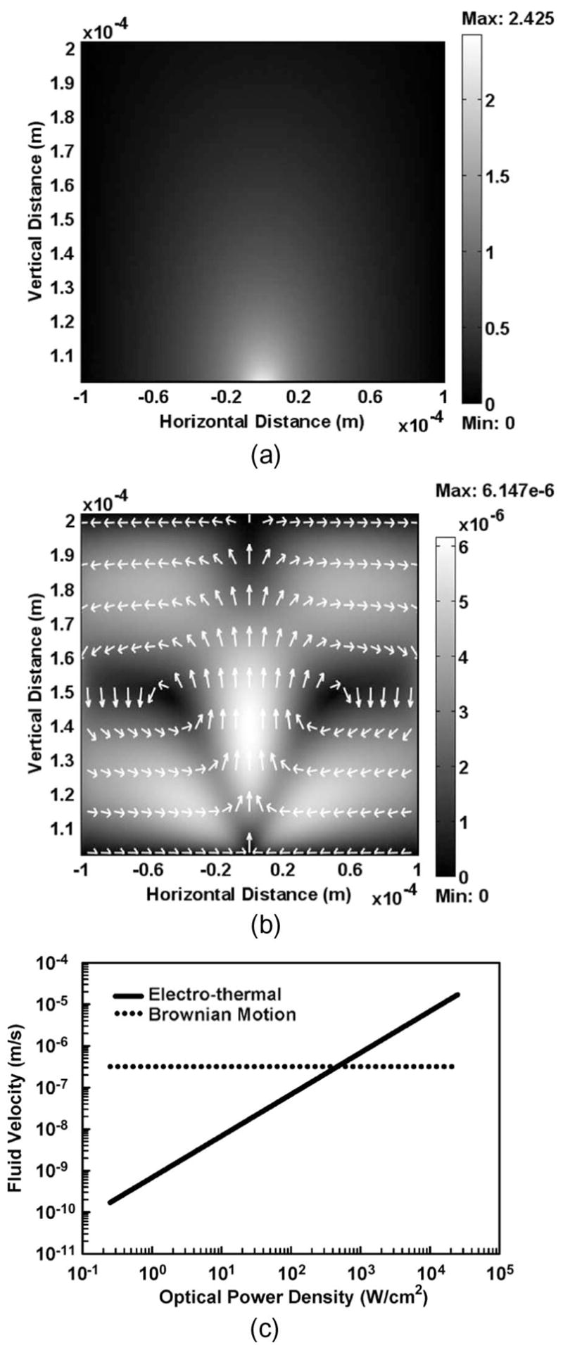
(a) Temperature increase distribution due to a 1-mW laser focused to a 20-μm spot size. (b) Simulated flow due to ET effects at 20 Vpp and 100 kHz, with an optical-power density of 250 W/cm2. (c) Dependence of ET fluid velocity on incident optical-power density at 20 Vpp and 100 kHz.
By calculating the temperature distribution for a given optical-power density and bias, (7) can be entered into the Navier–Stokes equation as a perturbing force, and the resulting fluid flow can be observed [Fig. 3(b)]. Bias conditions assume 20 Vpp and 100 kHz, with an optical-power density of 250 W/cm2. The maximum fluid velocity versus optical-power density (in the absence of all other effects) is shown Fig. 3(c) assuming a bias of 20 Vpp and 100 kHz. Notice that ET flow does not become prevalent for a 10-μm bead until the optical power is above 100 W · cm−2. In this figure, we linearly extrapolate the plot of Fig. 1(c) to predict the conductivities at high optical powers. This ignores the fact that the a-Si:H conductivity will saturate at high enough optical powers. Therefore, Fig. 3(c) provides a lower bound for when ET effects will occur.
The effects of ET flow will be dominant at high optical-power densities (higher temperature gradients) and high electric fields.
D. Buoyancy Effects
The density of a liquid is a function of temperature. Therefore, a localized temperature gradient can result in a fluid-density gradient which, under the influence of gravity, will result in fluid flow. This flow can be characterized by the following [18]:
| (8) |
where ρm is the fluid density, ΔT is the change in temperature, and g is the acceleration due to gravity (9.8 m · s−2).
Unlike the other effects aforementioned, this flow can occur in the OET device in the absence of applied bias. Thus, given a high enough temperature gradient, it is possible to move objects in the absence of applied bias.
This force, like the ET force, is entered into the Navier–Stokes equation as a fluidic perturbation. The resulting fluid flow is shown in Fig. 4(a) at 20 Vpp, 100 kHz, and 250 W/cm2. The maximum fluid velocity versus optical power density is shown in Fig. 4(b) at 20 Vpp and 100 kHz.
Fig. 4.
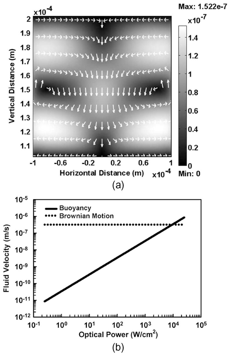
(a) Simulated fluid flow due to buoyancy effects at 20 Vpp, 100 kHz, and 250 W/cm2. (b) Dependence of buoyancy fluid velocity on optical-power density at 20 Vpp and 100 kHz. Note that the fluid velocity due to buoyancy is much smaller than that imposed by the other effects.
As one can see, the magnitude of buoyancy-driven flow is much less than the other effects. Buoyancy does not exceed Brownian motion for a 10-μm bead until the optical power is above 104 W · cm−2. However, one should note that the flow pattern is antiparallel to that of both ET and LACE. This will result in a minimum in the fluid velocity, as buoyancy is overcome by the other effects. As explained earlier, the a-Si:H conductivity has been linearly extrapolated for high optical-power densities from Fig. 1(c).
Therefore, we do not expect buoyancy to play a role in OET operation except in the absence of external biasing.
III. Development of a Figure of Merit
In order to determine which of the aforementioned effects is dominant for a given set of device and bias conditions, a figure of merit must be developed. Since all of the effects described eventually manifest themselves as a fluid or particle velocity, it is natural for the figure of merit to be a function of velocity. Specifically, we can compare the speed due to DEP to that induced by other effects in the fluid. Thereby, we define a dimensionless value β for each point in the liquid as
| (9) |
where XDEP, XEXT, and 〈XBROWNIAN〉 refer to the distance the particle travels in 1 s due to DEP, external forces (LACE, ET, and buoyancy), and Brownian motion, respectively. The average distance a spherical particle travels in 1 s due to Brownian motion is [19]
| (10) |
Therefore, a β value close to one corresponds to near-complete dominance, or control, by the DEP force. Likewise, a β value near zero indicates that DEP has little control over the particle motion.
Applying this definition of β to the simulation grid, one receives a value of β for each point in the mesh. It is therefore necessary to reduce this array of β values down to a single number, or figure of merit. Thus, we define a number B as
| (11) |
where r is defined as a control radius, d is the thickness of the liquid layer, and A is the area of integration equal to 2 × r × d. The control radius is determined by the greatest radius from the beam center at which any particle perturbation is expected. Fundamentally, ignoring all other effects, DEP can induce a particle velocity at a distance, as shown in Fig. 5(a), from the beam center until it is overcome by Brownian motion. Fig. 5(b) shows this distance as a function of particle size. It can be seen that, for a 10-μm particle operating at 10 Vpp in 1-mS · m−1 solution, the control radius is about 240 μm. Therefore, for this particle in a device with a 100-μm 1-mS · m−1 liquid layer, we integrate β over an area equal to 2 × 240 × 100 μm3 and then divide by this area.
Fig. 5.
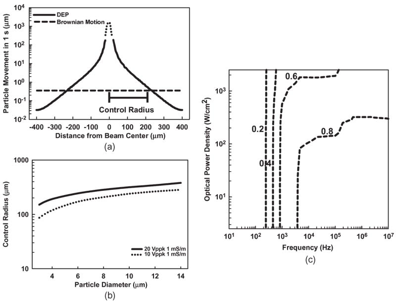
(a) Definition of control radius. The dotted region corresponds to points within 18 μm of the beam center which are not valid due to the effects of vertical DEP forces acting on the particle. (b) Dependence of control radius on particle size for 1-mS · m−1 solution biased at 20 and 10 Vpp. (c) Contour plot of B for a 10-μm particle in 1 mS · m−1 at 10 Vpp.
The control radius described earlier is difficult to measure experimentally. This is due to its definition. The control radius assumes that there are no external forces, outside of DEP and Brownian motion, acting on the particle. In reality, the other forces are always present to some degree. This greatly reduces the measured control radius relative to the experimental value. For example, for a 15-μm particle under the conditions listed for Fig. 5(b) at 20 Vpp, we measure a control radius of 190 μm. Theoretically, we expect a value of 280 μm. The discrepancy is due to the fact that, at large distances, other forces, namely, ET, counteract the relatively weak DEP force and, thus, reduce the measured control radius. Since the measured control radius is highly dependent on experimental setup, it is proposed that the theoretical control radius should be used in the calculation of B as it provides a more consistent and fundamental definition.
B is an average value of β over a predefined area. Therefore, it exists between zero and one and can be interpreted as the percent of DEP control for a given set of parameters. Fig. 5(c) shows a contour plot of B as a function of optical-power density and frequency for a typical set of device parameters and biasing. One can see that, for low frequencies and high optical-power densities, it is predicted that DEP has little control due to LACE and ET effects, respectively.
IV. Experimental Methods and Results
A. Device Under Test
The OET device used in this paper was fabricated on a commercially available glass substrate coated with a 300-nm layer of sputtered ITO with a sheet resistance of 10 Ω/□. A 2-μm layer of a-Si:H was then deposited in an Oxford Plasmalab 80plus plasma-enhanced chemical-vapor-deposition system. The process conditions for the a-Si:H recipe were as follows: 400-sccm Ar, 100-sccm SiH4, at a pressure of 900 mTorr, a temperature of 350 °C, and with an RF bias of 100 W. The a-Si:H layer thickness was chosen because at the excitation wavelength (635 nm); 90% of the incident light is absorbed within a distance of 1–2 μm.
Previous reported versions of the OET device have an ohmic-contact layer between the ITO and a-Si, as well as a thin nitride layer on top of the a-Si:H to combat stress issues. We have tuned the a-Si:H deposition to eliminate the stress and, thus, the need for the nitride layer. Additionally, the ohmic-contact layer was found to be unnecessary for the operation of the OET device.
The topside device consists of another piece of ITO-coated glass. The top and bottom device were separated by a 100-μm-thick spacer of double-sided tape. A 10-mW 635-nm diode laser in series with a continuous attenuator and 10× objective was used as the illumination source. Fig. 6 shows the experimental setup.
Fig. 6.
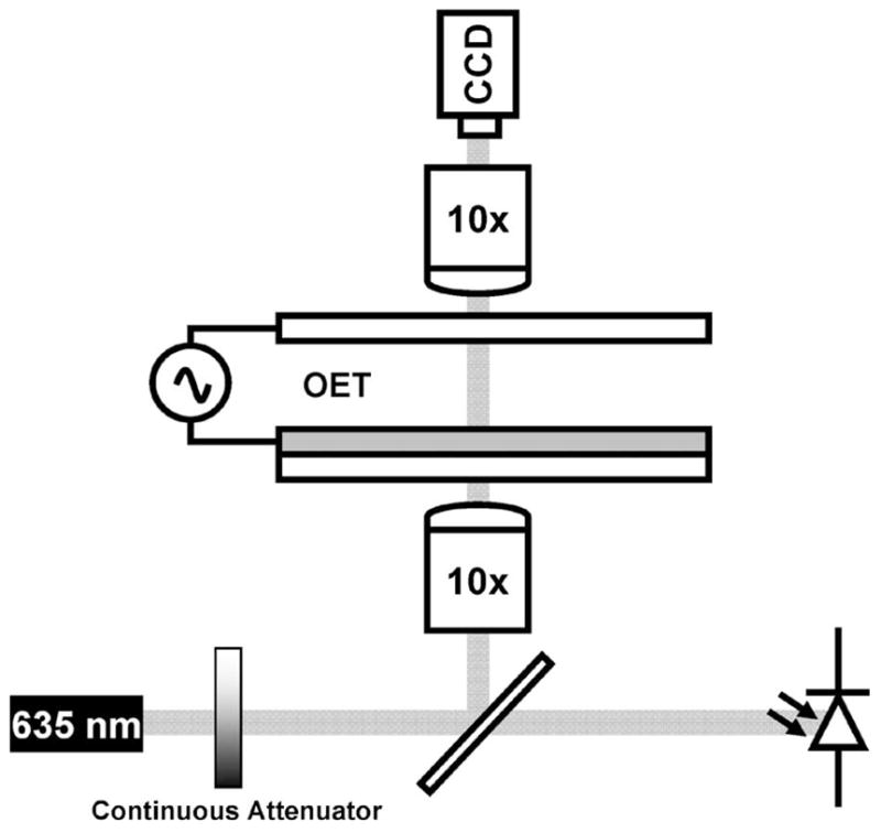
Depiction of experimental setup. A 635-nm diode laser is fed through a continuous attenuator followed by a 50/50 beam splitter. Half of the beam goes to a photodetector while the other half is sent through a 10× objective and is focused onto the device substrate. Observation occurs through a topside 10× objective connected to a CCD camera.
B. Methods
The device described earlier was subjected to a variety of bias points which varied in voltage, frequency, and optical power for a solution containing 10-μm polystyrene beads with a conductivity of 1 mS · m−1.
For each bias point, the dominant effect was recorded (DEP, LACE, ET, buoyancy, or Brownian motion). Video images of particle movement were analyzed, and the dominant effect was determined based on the following rules. DEP was defined as when a particle could be repelled greater than 5× its diameter from the beam center and not be moved further by any ambient-induced flow. LACE was differentiated from ET flow by assuming that if a flow-based effect was dominant for a frequency below 1 kHz, it was attributed to LACE. If flow was dominant at frequency higher than 1 kHz, it was then assumed to be ET in origin. Arguably, there is a gray area in the transition area around 1 kHz. In this region, both ET and LACE are simultaneously occurring, and it is very difficult to distinguish between the two. Buoyancy was ignored when a nonzero voltage was applied, as its effects are much less than the other forces present. If no significant particle response was recorded, it was assumed that Brownian motion was the dominant mechanism. Quite often, electrolysis of the liquid, in conjunction with LACE, occurred for low-frequency biasing. This is noted as LACE/electrolysis.
C. Experimental Results
The experimental and simulated results are shown in Fig. 7. Simulated values of B are plotted on a contour plot, while experimental results are overlaid as points. The simulation includes all of the aforementioned effects and assumes all the device dimensions described earlier.
Fig. 7.
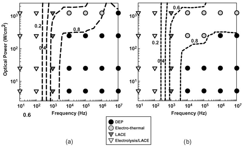
Overlay of observed dominant effect with theoretical predictions for 1 mS · m−1 at (a) 20 and (b) 10 Vpp. All DEP observations occur when the B value is greater than 0.8.
The experimental results follow the trends of the B contour lines. It appears that, for this liquid solution, a normalized B value of greater than 0.8 results in DEP actuation. DEP actuation, as predicated by the theory, is overcome by LACE at low frequencies, ET at high optical powers, and both LACE and ET at high optical powers and low frequencies. Therefore, it appears that, to ensure DEP dominance over external effects (e.g., LACE, ET, buoyancy), the OET device should be operated at frequencies above the LACE cutoff (~1 kHz for 1-mS · m−1 solution) and low optical-power densities (less than 1 kW · cm−2 for this device).
As one can see, a reduction in voltage (20–10 Vpp) reduces the overall DEP control range (i.e., the arc length of the contour line corresponding to a B of 0.8 shrinks). This is somewhat counterintuitive at first, since both DEP and ET scale with the square of the voltage (assuming most of the heat generation is due to laser absorption). However, the effect manifests itself as a competition between buoyancy-driven flow and ET flow. From Figs. 3(b) and 4(a), one can see that the flow directions are antiparallel to one another. Therefore, there will be a threshold voltage at which ET-driven flow will reverse the direction of the voltage-independent buoyancy-driven flow (it is assumed that LACE has negligible effect at the frequencies of interest, and Joule heating is negligible relative to laser heating). This results in a minimum fluid velocity. Due to this local minimum, DEP can control a larger area for higher applied voltages. This is shown in Fig. 8.
Fig. 8.
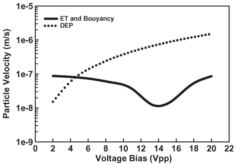
Comparison of simulated particle velocity due to ET and buoyancy effects. Competition between ET and buoyancy results in a localized minimum allowing DEP to have greater control at higher voltages.
V. Discussion
There are a variety of other parameters that affect the percentage of DEP control on a particle in the OET device. Perhaps most prevalent is particle size. The DEP force scales as the cube of particle radius. Since the other effects do not scale with particle size (aside from Brownian motion), the relative contribution of DEP to particle control will decrease sharply with decreasing particle diameter. However, we have only considered particles which exhibit negative DEP. Certain particles have positive CM factors which result in an attractive force toward the illuminated region. In this case, it is conceivable that external forces can actually aid in particle trapping. This is because external fluid flow, such as LACE or ET, can bring the particle of interest toward the beam where it is trapped by the strong DEP force near the beam center. In these cases, smaller particles may be able to be trapped via DEP despite relatively small forces outside of the beam center. Additionally, particle geometry plays a role. For example, nanowires exhibit a much larger CM factor due to their cylindrical shape. Therefore, it is possible to use DEP to trap and manipulate individual nanowires [20].
It is also possible to alter the device geometry to control smaller particles with DEP. By decreasing the thickness of the liquid layer, a larger electric-field gradient is produced, which results in an increased DEP force. This technique can be used for the manipulation of very small particles. However, for certain biological applications, such as cell manipulation, the gap spacing must be large enough to enable the viability of the cells themselves.
Another major parameter of interest is liquid conductivity. The OET device relies on the ability to switch voltage to the liquid layer upon illumination. If the liquid conductivity increases, the amount of voltage switched to the liquid layer will decrease. Therefore, DEP actuation is decreased for high liquid conductivity. This is an area of concern because many of the biological applications of OET require the use of high-conductivity media. As a result, a method of increasing the effects of the light-actuated switching mechanism is needed. One way to accomplish manipulation in high-conductivity media is to replace the photoconductive layer by a phototransistor structure [21]. With the added gain of the phototransistor, voltage can be more efficiently switched to the liquid layer, resulting in DEP actuation even in high-conductivity media.
VI. Conclusion
We have presented a framework for the forces present during the use of OET. It is clear that a multitude of physical effects is present in the OET device. These effects manifest themselves in different operating regimes.
By developing a figure of merit to quantify the relative contributions due to each of these forces, we are able to accurately predict where DEP actuation is most likely to occur for a set of bias and device parameters.
Depending on bias conditions, the particles in the OET device will be influenced by a variety of effects. These include LACE, ET, buoyancy, and DEP. LACE dominates for low frequencies, while ET is prevalent at high optical powers. Thus, for the device discussed here, in order to insure DEP actuation, the optical-power density must be kept below 100 W · cm−2, the voltage should be in the range of 10–20 Vpp, and the bias frequency must be above the LACE cutoff of approximately 1 kHz.
Acknowledgments
All devices were fabricated in the UC Berkeley Micro-fabrication Laboratory.
This work was supported in part by the National Institutes of Health under the NIH Roadmap for Medical Research Grant PN2 EY018228 and in part by the Center for Cell Mimetic Space Exploration (CMISE) under Award NCC 2-1364. Subject Editor S. Shoji.
Biographies
Justin K. Valley received the B.S. degree in electrical engineering from the University of Michigan, Ann Arbor, in 2006. He is currently working toward the Ph.D. degree in electrical engineering in the Electrical Engineering and Computer Science Department, Berkeley Sensor and Actuator Center, University of California, Berkeley.
His research interests include the areas of microfluidics and optical and biological microelectromechanical systems.

Arash Jamshidi received the B.S. degree in electrical engineering from Simon Fraser University, Vancouver, BC, Canada, in 2005.
He is currently a Graduate Student Researcher with the Electrical Engineering and Computer Science Department, Berkeley Sensor and Actuator Center, University of California, Berkeley, under the supervision of Prof. M. C. Wu. He is currently working on optoelectronic-tweezers applications in the nanoscale. His research interests include nanotechnology, optoelectronics, and biological microelectromechanical systems.
Aaron T. Ohta (S’99) received the B.S. degree in electrical engineering from the University of Hawai’i at Manoa, Honolulu, in 2003, and the M.S. degree in electrical engineering from the University of California at Los Angeles, Los Angeles, in 2004. He is currently working toward the Ph.D. degree in electrical engineering in the Electrical Engineering and Computer Science Department, Berkeley Sensor and Actuator Center, University of California, Berkeley.
His research interests include microelectromechanical systems (MEMS) and bioMEMS.
Mr. Ohta was the recipient of a National Science Foundation (NSF) Graduate Research Fellowship.

Hsan-Yin Hsu received the B.S. degree from the Department of Electrical Engineering, Purdue University, West Lafayette, IN, in 2005. He is currently working toward the Ph.D. degree in the Electrical Engineering and Computer Science Department, Berkeley Sensor and Actuator Center, University of California, Berkeley.
His research interests are in microelectromechanical systems, microfluidics, and optical systems for biomedicine application.
Ming C. Wu (S’82–M’83–SM’00–F’02) received the M.S. and Ph.D. degrees in electrical engineering from the University of California, Berkeley, in 1985 and 1988, respectively.
From 1988 to 1992, he was a member of Technical Staff with AT&T Bell Laboratories. From 1992 to 2004, he was a Professor with the Electrical Engineering Department, University of California, Los Angeles. In 2004, he joined the University of California, Berkeley, where he is currently a Professor in the Electrical Engineering and Computer Science Department, Berkeley Sensor and Actuator Center (BSAC). He is also currently a Codirector of BSAC. His research interests include micro- and nanoelectromechanical systems, optofluidics, optoelectronics, nanophotonics, and biophotonics. He has published six book chapters, 140 journals, and 300 conference papers. He is the holder of 16 U.S. patents.
Dr. Wu is a member of the Optical Society of America. He was a Packard Foundation Fellow from 1992 to 1997. He was the recipient of the 2007 Engineering Excellence Award from the Optical Society of America.

References
- 1.Ashkin A. Optical trapping and manipulation of neutral particles using lasers. Proc Nat Acad Sci USA. 1997 May;94(10):4853–4860. doi: 10.1073/pnas.94.10.4853. [DOI] [PMC free article] [PubMed] [Google Scholar]
- 2.Grier DG. A revolution in optical manipulation. Nature. 2003 Aug;424(6950):810–816. doi: 10.1038/nature01935. [DOI] [PubMed] [Google Scholar]
- 3.Fiedler S, Shirley SG, Schnelle T, Fuhr G. Dielectrophoretic sorting of particles and cells in a microsystem. Anal Chem. 1998 May;70(9):1909–1915. doi: 10.1021/ac971063b. [DOI] [PubMed] [Google Scholar]
- 4.Gascoyne PRC, Vykoukal J. Particle separation by dielectrophoresis. Electrophoresis. 2002 Jul;23(13):1973–1983. doi: 10.1002/1522-2683(200207)23:13<1973::AID-ELPS1973>3.0.CO;2-1. [DOI] [PMC free article] [PubMed] [Google Scholar]
- 5.Chiou PY, Ohta AT, Wu MC. Massively parallel manipulation of single cells and microparticles using optical images. Nature. 2005 Jul;436(7049):370–372. doi: 10.1038/nature03831. [DOI] [PubMed] [Google Scholar]
- 6.Ohta AT, Chiou PY, Han TH, Liao JC, Bhardwaj U, McCabe ERB, Yu F, Sun R, Wu MC. Dynamic cell and microparticle control via optoelectronic tweezers. J Microelectromech Syst. 2007 Jun;16(3):491–499. [Google Scholar]
- 7.Choi W, Kim SH, Jang J, Park JK. Lab-on-a-display: A new microparticle manipulation platform using a liquid crystal display (LCD) Microfluidics Nanofluidics. 2007 Apr;3(2):217–225. [Google Scholar]
- 8.Lu YS, Huang YP, Yeh JA, Lee C, Chang YH. Controllability of non-contact cell manipulation by image dielectrophoresis (iDEP) Opt Quantum Electron. 2005 Dec;37(13–15):1385–1395. [Google Scholar]
- 9.Neale SL, Mazilu M, Wilson JIB, Dholakia K, Krauss TF. The resolution of optical traps created by light induced dielectrophoresis (LIDEP) Opt Express. 2007 Oct;15(20):12 619–12 626. doi: 10.1364/oe.15.012619. [DOI] [PubMed] [Google Scholar]
- 10.Chiou PY, Ohta AT, Jamshidi A, Hsu H-Y, Chou JB, Wu MC. Light-actuated AC electroosmosis for optical manipulation of nanoscale particles. Proc. Solid-State Sens., Actuators, Microsyst. Workshop; Hilton Head Island, SC. 2006. pp. 56–59. [Google Scholar]
- 11.Pohl HA. Dielectrophoresis: The Behavior of Neutral Matter in Nonuniform Electric Fields. New York: Cambridge Univ. Press; 1978. [Google Scholar]
- 12.Jones TB. Electromechanics of Particles. Cambridge, U.K: Cambridge Univ. Press; 1995. [Google Scholar]
- 13.Lyklema J. Fundamentals of Interface and Colloid Science. Vol. 2. London, U.K: Academic; 1991. [Google Scholar]
- 14.Wang P, Chen ZL, Chang HC. A new electro-osmotic pump based on silica monoliths. Sens Actuators B, Chem. 2006 Jan;113(1):500–509. [Google Scholar]
- 15.Ramos A, Morgan H, Green NG, Castellanos A. AC electric-field-induced fluid flow in microelectrodes. J Colloid Interface Sci. 1999 Sep;217(2):420–422. doi: 10.1006/jcis.1999.6346. [DOI] [PubMed] [Google Scholar]
- 16.Chiou PY. Ph.D. dissertation, Univ. California Berkeley; Berkeley, CA: 2005. Massively parallel optical manipulation of single cells, micro- and nano-particles on optoelectronic devices. [Google Scholar]
- 17.Castellanos A, Ramos A, Gonzalez A, Green NG, Morgan H. Electrohydrodynamics and dielectrophoresis in microsystems: Scaling laws. J Phys D, Appl Phys. 2003 Oct;36(20):2584–2597. [Google Scholar]
- 18.Ramos A, Morgan H, Green NG, Castellanos A. AC electrokinetics: A review of forces in microelectrode structures. J Phys D, Appl Phys. 1998 Sep;31(18):2338–2353. [Google Scholar]
- 19.Einstein A. Investigations on the Theory of Brownian Movement. New York: Dover; 1956. [Google Scholar]
- 20.Jamshidi A, Pauzauskie PJ, Ohta AT, Chiou PY, Hsu H-Y, Yang P, Wu MC. Semiconductor nanowire manipulation using optoelectronic tweezers. Proc. 20th IEEE In. Conf. MEMS, Kobe; Japan. 2007. pp. 155–158. [Google Scholar]
- 21.Hsu HY, Ohta AT, Chiou PY, Jamshidi A, Wu MC. Phototransistor-based optoelectronic tweezers for cell manipulation in highly conductive solution. Proc. 14th Int. Conf. Transducers; Lyon, France. 2007. pp. 477–480. [Google Scholar]