Abstract
The static and dynamic characteristics of a bimorph deformable mirror (DM) for use in an adaptive optics system are described. The DM is a 35-actuator device composed of two disks of lead magnesium niobate (PMN), an electrostrictive ceramic that produces a mechanical strain in response to an imposed electric field. A custom stroboscopic phase-shifting interferometer was developed to measure the deformation of the mirror in response to applied voltage. The ability of the mirror to replicate optical aberrations described by the Zernike polynomials was tested as a measure of the mirror’s static performance. The natural frequencies of the DM were measured up to 20 kHz using both stroboscopic interferometry as well as a commercial laser Doppler vibrometer (LDV). Interferometric measurements of the DM surface profile were analyzed by fitting the surface with mode-shapes predicted using classical plate theory for an elastically supported disk. The measured natural frequencies were found to be in good agreement with the predictions of the theoretical model.
Keywords: Adaptive optics, Deformable mirrors, Interferometry, Micromechanical devices
1. Introduction
Originally developed to remove atmospheric distortion from astronomical imaging systems, adaptive optics (AO) has seen more recent application to ophthalmologic instruments and free-space optical communication systems. In each of these applications, the AO system uses a deformable mirror (DM) to correct for optical aberrations by removing phase distortions from the incident wavefront. Since the existing DM technology developed for astronomy is expensive and bulky, recent research has focused on using micro-electromechanical (MEMS) technology to create a more compact, low-cost DM. Several MEMS DM designs have been demonstrated, including: membrane-based (OKO Technologies Inc.) [1]; polysilicon surface-micromachined (Boston Micromachines Inc.) [2]; bulk silicon (Iris AO Inc.) [3]; and piezoelectric monomorphs Jet Propulsion Laboratory [4].
The ability of a DM to correct for a particular optical aberration is determined by the aberration’s spatial frequency and amplitude. Roughly speaking, the maximum spatial frequency that a DM may correct is determined by the number of actuators, while the maximum correctable amplitude is dependent on the type of DM employed. For a segmented DM, the maximum correction amplitude depends only on actuator stroke and is independent of spatial frequency, whereas for continuous face-sheet and bimorph DMs, the correction amplitude depends on the imposed spatial frequency.
Many MEMS DM designs have been driven by the motivation to produce wavefront correctors with hundreds or thousands of actuators. For applications which require the correction of only low-order aberrations (such as defocus, astigmatism, coma, and spherical aberration), a DM with less than 100 actuators may be the best choice, as such a device can be lower in cost and complexity than a DM with higher actuator count. There is some evidence that such a low order DM may provide sufficient correction for opthalmological AO applications. Defocus and astigmatism, which are second-order aberrations, represent 92% of the total wavefront aberrations found in subjects with normal vision [5], and the aberration magnitude diminishes with increasing radial order. The dominant higher order aberrations are coma and spherical aberration, which are third- and fourth-order aberrations and account for 1.8% and 1.6% of the total RMS wavefront error, respectively [6].
We have chosen to investigate the characteristics of bimorph DMs in an effort to understand their suitability for opthalmological AO applications. This class of DM is capable of correcting very large amplitude, low-order aberrations, and is simple to construct, a fact that should ultimately result in a low-cost DM [7]. The drawback of the bimorph design is that the maximum correctable amplitude diminishes strongly with increasing spatial frequency [8]. For this reason, the bimorph DM is unlikely to be suitable for systems requiring correction of very high-order aberrations. However, the bimorph may satisfy the requirements of opthalmological AO, where correction of aberrations up to the fifth radial-order may be sufficient.
We have tested three bimorph DMs manufactured by AOptix (Campbell, CA), each having similar characteristics with the exception of small manufacturing differences [9,10]. One of these units has been successfully employed in an AO system for in vivo retinal imaging [11]. Additionally, Dalimier and Dainty recently showed that the AOptix DM was superior to two other DMs when used to correct for synthetic aberrations typical of those found in the human eye [12].
2. Methods
Tests were performed using a commercial laser-Doppler vibrometer (LDV) and a custom-built stroboscopic phase-shifting interferometer, described below. Our first objective was to characterize the maximum correction amplitude that the DM could produce as a function of spatial frequency. To this end, we developed a method to use the DM to reproduce optical aberrations described by the Zernike polynomials [13]. Next, we studied the dynamic characteristics of the DM and experimentally measured the natural vibration modes.
2.1. Bimorph DM design
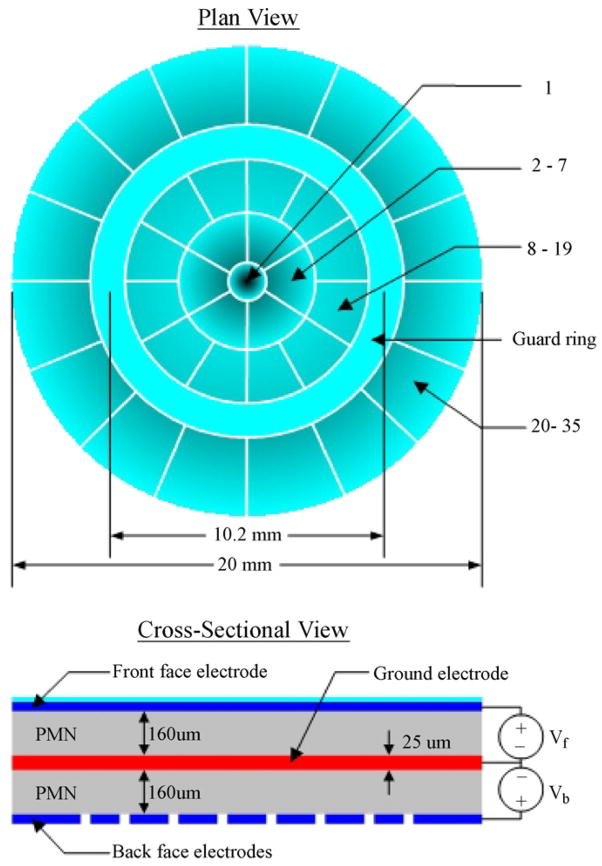
The layout of the AOptix DM is illustrated in plan view and cross-section in Fig. 1. The device is composed of two 160 μm thick layers of the electrostrictive ceramic lead magnesium niobate (PMN). Metal electrodes are deposited onto the PMN and the two layers are bonded together with a 25 μm thick layer of conductive adhesive. The metallization on the back face of the DM is patterned to produce 36 electrodes, while the uniform metallization on the front face of the DM produces a single front face electrode. The DM is 20 mm in diameter, with only the center 10.2 mm of the DM used as an optical surface in order to reduce the effect of the edge supports on the DM surface profile.
Fig. 1.
Layout of the AOptix DM: plan view of electrodes (top) and cross-sectional view (bottom). The numbering of the actuator channels is indicated on the plan view.
As illustrated in the figure, voltage is applied to the electrodes on the front and back faces of the DM, with the inner bonded electrodes serving as ground contacts for both layers. The electrodes on the back face of the DM consist of a central pad surrounded by four annular rings of electrodes. The central pad and the electrodes in the two inner rings (channels 1–19) are used to generate local curvature in the mirror surface, while the electrodes in the outer ring (channels 20–35) produce a slope at the edge of the DM. The curvature and slope electrodes are separated by the third annular electrode ring which defines the 10 mm pupil. The completed mirror assembly is mounted in a housing with manual tip-tilt adjustment and a 10.2 mm clear aperture.
PMN is a relaxor ferroelectric material that displays electrostrictive behavior near room temperature [14]. Like piezoelectric materials such as lead zirconium titanate (PZT), electrostrictive materials deform mechanically when an electric field is applied to the material. In contrast to piezoelectrics, in which the direction of deformation reverses with the polarity of the applied field, in electrostriction the deformation direction is independent of the sign of the applied electric field. Although a wide variety of dielectrics possess electrostrictive properties, the effect is particularly large in the relaxor ferroelectrics like PMN. When an electric field is applied to PMN, the material contracts along the transverse axes. In comparison with PZT, PMN has the advantage of greater linearity and lower hysteresis at room temperature.
In the bimorph structure, voltage applied across the top layer generates a tensile stress in the top layer, causing the bimorph to undergo a concave curvature. Similarly, voltage applied across the bottom layer results in convex curvature. Because the front face electrode has a capacitance that is more than 36 times greater than the capacitance of the individual back face electrodes, driving this electrode at high frequencies requires considerably greater power and current from the high voltage drive amplifiers. As a result, when employed in a high bandwidth AO system, the front face electrode is normally biased at a constant voltage, and only the back-face electrode voltages are varied. In the absence of any residual stress in the two layers, the DM surface is flat whenever an equal voltage is applied across both the top and bottom layers. Local convex (or concave) surface deformations are then produced by setting the potential on the individual back face electrodes above (or below) the potential on the front face electrode. To allow symmetric convex/concave actuation, the front-face potential is normally set to approximately the middle of the output span of the high-voltage amplifiers. Residual stress from the manufacturing process results in a slight parabolic curvature to the DM surface when all the electrodes are at the same potential. This initial curvature is removed by applying a small voltage difference between the front and back face electrodes. We have tested three DM units and each required slightly different voltage settings to flatten the DM.
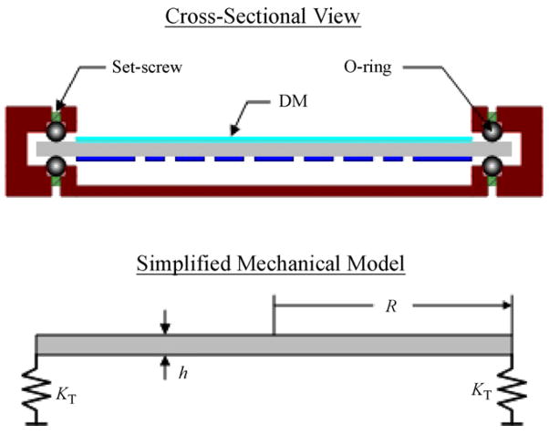
Mounting a bimorph DM is a challenging problem, since any constraint at the edges of the DM will reduce the curvature which can be achieved. The AOptix DM is mounted using two rubber o-rings which are preloaded by multiple set-screws arrayed at the outer edge of the mirror [15], as illustrated in Fig. 2. The o-ring mount produces translational compliance and near-zero rotational compliance at the DM edge, as described further below.
Fig. 2.
Cross-sectional view of the DM mount (top) and simplified mechanical model for the DM edge supports (bottom).
2.2. Phase-shifting interferometer
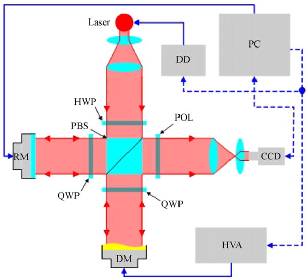
Dynamic and static measurements of the surface profile of the DM were collected using a stroboscopic phase-shifting interferometer. A block-diagram of the instrument is illustrated in Fig. 3. The instrument is a Twyman–Green interferometer in which a piezoelectric stage (Polytec PI P-753.11C) translates a reference mirror in order to introduce a controlled phase-shift between the light passing through the reference and measurement arms of the interferometer. Surface height variations in the DM create interference fringes when the reference and measurement beams are recombined, producing an interferogram that is captured and digitized using a CCD camera (Cohu 6612–1000) and a frame-grabber card (Matrox Meteor-II). The surface profile of the DM is reconstructed using five interferograms collected at four distinct phase shifts (0, π/2, π, 3π/2) using Hariharan’s algorithm [16]. The use of a similar instrument for dynamic characterization of millimeter-sized MEMS devices was first described by Hart et al. [17]. The instrument is capable of measuring the surface profile with an RMS accuracy of approximately 6 nm and an absolute accuracy of ±60 nm across a 10 mm pupil.
Fig. 3.
Stroboscopic interferometer block-diagram. RM: reference mirror, HWP: half-wave plate, QWP: quarter-wave plate, PBS: polarizing beam-splitter, POL: polarizer, DM: deformable mirror, HVA: high voltage amplifier, DD: digital delay.
The interferometer was outfitted with a pulsed diode laser to allow the DM surface profile to be measured in response to time-varying voltage inputs. The 10 mW laser (Hitachi HL6320G) is driven with a custom current source capable of producing optical pulses of less than 1 μs duration. Strobing the illumination source gates the image, allowing motion at frequencies much faster than the CCD frame rate (30 Hz) to be measured. The strobed illumination is synchronized to the high voltage line used to drive one of the actuators on the DM, and a programmable digital delay unit (Directed Energy model PDG-2510) is used to control the time delay (Δt) between the applied voltage and the optical pulse. By varying Δt, images of the DM surface at various times throughout the actuation cycle are obtained. Ideally, the optical pulse is sufficiently fast that the DM is essentially motionless during the measurement interval; any motion of the mirror surface during this interval reduces the contrast of the interference fringes and introduces error in the surface measurement. Assuming that the DM undergoes a 1 μm amplitude, 10 kHz sinusoidal oscillation, the maximum motion of the mirror surface over a 1 μs interval is approximately 63 nm. This is approximately λ/10 for a 635 nm diode laser, representing a small but acceptable reduction in contrast.
2.3. Open-loop generation of Zernike modes
To characterize the dependence of the DM stroke on the spatial frequency of deformation, a simple open-loop control method was developed. In this approach, the deformation of the DM surface is modeled as a weighted combination of the deformations contributed by each actuator channel, known as the actuator influence function. The deformation of the DM surface, w(r, θ), is described by
| (1) |
where N represents the number of actuators on the DM, ϕi(r, θ) is the influence function and νi is the control voltage applied to the i-th actuator, while f (νi) represents the normalized actuator displacement as a function of applied voltage. In the special case that the actuator displacement varies linearly with applied voltage, f (νi) may be replaced by (νi/νmax) in (1). In vector-matrix form, (1) becomes:
| (2) |
where ϕ⃗(r, θ) = [ϕ1(r, θ), ϕ2(r, θ),…, ϕN (r, θ)] and ν⃗ = [ν1, ν2,…, νN]. In electrostrictive and piezoelectric bimorphs, the displacement is a nonlinear function of applied voltage. To approximate f (νi), we drove all the actuators at the same voltage and measured the DM displacement as a function of applied voltage. This method does not account for any variation between different actuators, but does account for the general saturation characteristics of the PMN ceramic.
The influence function for each of the N = 35 back face electrodes was measured by applying νmax to the desired channel and interferometrically measuring the resulting DM surface shape. The guard ring was not utilized in these tests and was held at a constant potential equal to that of the front face electrode. Each measured influence function was then approximated with an M-dimensional combination of Zernike polynomials through a least-squares fit [18]:
| (3) |
where zj(r, θ) is the j-th Zernike polynomial, and the aij’s are the coefficients used to fit the i-th influence function. Piston, the 0-th order polynomial, was discarded after the least-squares fit. Expressed in vector-matrix form:
| (4) |
where z⃗(r · θ) = [z1(r · θ), z2(r · θ),…, zM(r · θ)] is the 1 × M vector of Zernike polynomials and A is the N × M influence matrix. The present work explores using the DM to generate 20 Zernike mode shapes up to the fifth radial order, so the maximum fit length was M = 20, resulting in a 35 × 20 A matrix. When A is decomposed using the singular-value decomposition (SVD), the magnitude of each singular value provides an indication of the DM’s ability to reproduce each Zernike mode—singular values near zero indicate modes which are not controllable with the DM. The SVD is used to compute A*, the pseudo-inverse of A, which in turn is used to calculate the vector of control voltages, ν⃗, required to reproduce the desired combination of Zernike mode shapes. If the 1 × M vector e⃗ represents the desired combination of Zernike modes, the required control voltages can be calculated from:
| (5) |
Since f (νi) is not generally invertible, the function is approximated using a fifth-order polynomial fit of the measured voltage to displacement curve and the inversion is performed using a look-up table which maps actuator displacement to control voltages. In the case where the actuator displacement varies linearly with applied voltage, (5) becomes:
| (6) |
2.4. Modal response model
To study the dynamic response of the mirror surface to input voltage pulses, the free vibration of the DM was analyzed using classical plate theory. Approximating the DM as a thin, uniform, circular plate of PMN, the free vibration of the DM, w(r, θ, t), is described by the following fourth-order differential equation:
| (7) |
where D = Eh3/(12(1 − ν2)) denotes the flexural stiffness, and E, ν, ρ, h are the Young’s modulus (61 GPa), Poisson’s ratio (0.3), density (7.8 g/cm3), and thickness of the DM (345 μm). When the plate deflection is decomposed into a spatially varying and a temporally varying component, so that w(r, θ, t) = u(r, θ) exp(jωt), the spatial solutions to (7) are mode shapes of the following form:
| (8) |
where Amn is a normalization constant, Bmn a mode shape parameter, βmn an eigenvalue, Jm and Im denote the m-th order Bessel function of the first kind and the m-th order hyperbolic Bessel function of the first kind, respectively. The eigenvalues of (8) are related to the natural frequencies of the DM by
| (9) |
where R is the radius of the DM.
Values for the constants Amn, Bmn, and βmn can be calculated by applying the boundary conditions imposed by the DM mount. These constants were computed using the solution developed by Zagrai and Donskoy for a plate with elastic supports [19]. The translational stiffness of the o-ring support was modeled by first computing the deflection, δ, of the o-ring due to a load per unit length, p, using a Hertzian contact model of a cylinder compressed between two flat surfaces [20]:
| (10) |
where V = (1 − ν2)/( πE), ν is Poisson’s ratio for the rubber oring (0.5), E the Young’s modulus for rubber (1.7 MPa), d the cross-sectional diameter of the o-ring (1 mm), and R is the radius of the o-ring (10 mm). These material constants for the o-ring were estimated based on typical o-ring characteristics and result in reasonable agreement with the experimental data. A linearized compliance per unit length, CT, was calculated from the slope of the load-deflection model (10) at a given pre-load per unit length, p0:
| (11) |
CT is relatively insensitive to changes in the pre-load since it has a logarithmic dependence on this parameter. We assumed a pre-load per unit length of 0.16 N/mm. Taking into account the o-rings on both surfaces of the mirror and multiplying the stiffness per unit length by the circumference of the o-rings, the total translational stiffness of the mount was found to be:
| (12) |
In addition to the flexural natural frequencies described by (9), the DM also has a rigid-body mode due to the DM vibrating in the mirror mount. The natural frequency of this mode is given by
| (13) |
where m denotes the mass of the mirror (0.85 g).
3. Results and discussion
3.1. Static measurements
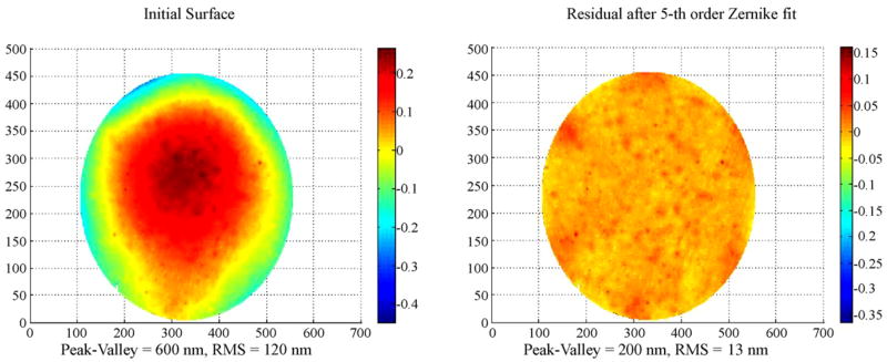
Preliminary measurements of the nominally flat DM surface were obtained with the front face and all back face electrodes set to 100 V. The resulting surface height map, illustrated in Fig. 4, shows a variation of 600 nm peak-to-valley and 120 nm RMS. To isolate the effects of low spatial frequency variations which could theoretically be removed in a closed-loop AO system from the high spatial frequency surface roughness of the mirror, the data were fit using a fifth-order Zernike approximation. The residual error after this fit is illustrated in the figure and shows that a variation of 200 nm peak-to-valley and 13 nm RMS remains. The primary source of this residual surface roughness is small pits with a depth of approximately 150 nm and a diameter of 100–200 μm. These pits are attributed to defects in the surface produced when the ceramic surface of the DM is polished during manufacturing.
Fig. 4.
Measurements of flat DM. Left: measured mirror surface. Right: the residual error after a fifth order Zernike fit to the measured surface.
3.1.1. Maximum stroke
Although the front face electrode is nominally biased at 100 V and the back face electrodes are used to control the DM shape, the maximum parabolic deformation is obtained when the electric field-induced stress in either the top or bottom ceramic layer is minimized (by setting the potential across this layer to 0 V) while the stress in the other layer is maximized (by setting the potential to νmax = 300 V). This fact was utilized to characterize the maximum stroke available for defocus. The maximum convex deformation, measured at 20.8 μm, is produced when the front face electrode is driven to 300 V while all back face electrodes (channels 1–35 and the guard ring) are grounded. Similarly, the maximum concave deformation, measured at 19.3 μm, is produced when the front face electrode is grounded while all back face electrodes are driven to 300 V. These parabolic deformations correspond to defocus values of −3.2 Diopters and +3.0 Diopters when measured across the 10.2 mm pupil.
3.1.2. Linearity
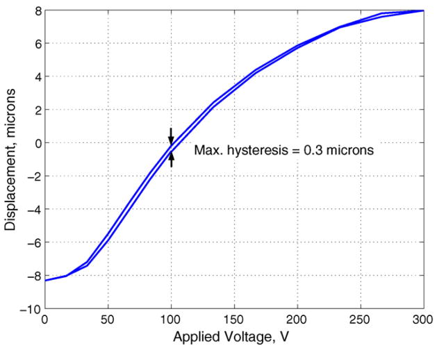
The linearity and hysteresis of the actuator characteristics were measured by holding the front face and guard ring electrodes at the nominal 100 V bias voltage and driving all the back face electrodes from 0 to 300 V and back again. The results of this test are shown in Fig. 5. At voltages below approximately 50 V, the mirror deformation displays a quadratic dependence on the applied voltage. Voltages from 50 to 200 V result in a nearly linear displacement characteristic, and the polarization of the ceramic begins to saturate above 200 V, with very little displacement occurring for voltages above 250 V (E ≈ 1500 V/mm). The actuator hysteresis was measured to be 0.3 μm, approximately 2% of the full-scale peak-to-peak displacement of 16 μm.
Fig. 5.
Measurement of actuator linearity and hysteresis. The front face and guard ring electrodes are held at 100 V while all the remaining back face electrodes (channels 1–35) are driven from 0 to 300 V.
3.2. Reproduction of Zernike mode shapes
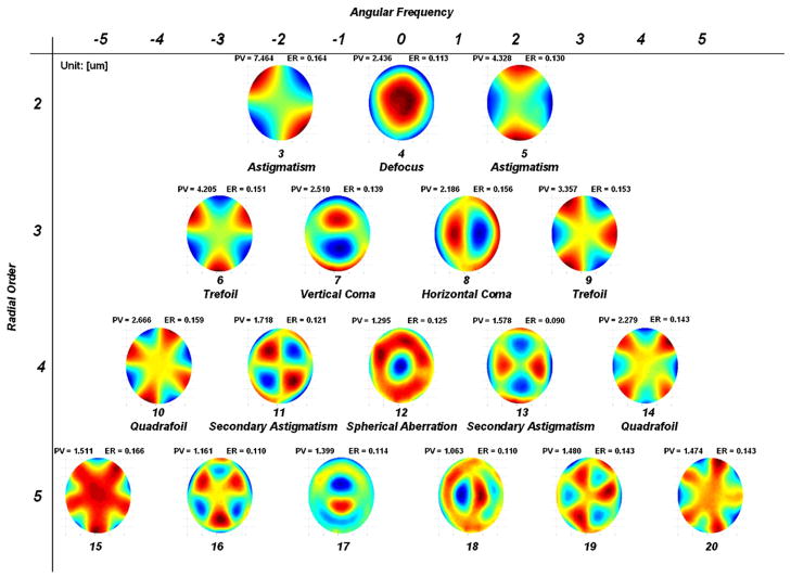
Eq. (5) was used to calculate the control voltages required to generate each Zernike mode shape up to the fifth order. To determine the maximum peak-to-valley (PV) displacement achievable for each mode, the amplitude of each mode was progressively increased in the input vector e⃗ until the computed control voltage on any one actuator channel exceeded the maximum limits available from the high-voltage amplifier. The results of the open-loop mode shape generation tests are summarized in Fig. 6 and Table 1.
Fig. 6.
Replication of Zernike mode shapes using the open-loop control method. The maximum PV amplitude and RMS residual error (ER) are indicated for each mode.
Table 1.
Summary of maximum stroke and RMS error for generated Zernike modes
| Radial order | Angular frequency | Description | Peak-valley (μm) | RMS error (μm) |
|---|---|---|---|---|
| 2 | −2 | Astigmatism (−45 and +45) | 7.464 | 0.164 |
| 0 | Defocus | 3.232a | 0.264 | |
| +2 | Astigmatism (0 and 90) | 6.078a | 0.304 | |
| 3 | −3 | Trefoil 1 | 4.205 | 0.151 |
| −1 | Vertical Coma | 2.510 | 0.139 | |
| +1 | Horizontal Coma | 2.186 | 0.156 | |
| +3 | Trefoil 2 | 3.357 | 0.153 | |
| 4 | −4 | Quadrafoil 1 | 2.749 | 0.156 |
| −2 | Secondary astigmatism 1 | 1.718 | 0.121 | |
| 0 | Spherical aberration | 1.295 | 0.125 | |
| +2 | Secondary astigmatism 2 | 1.578 | 0.090 | |
| +4 | Quadrafoil 2 | 2.279 | 0.143 | |
| 5 | −5 | Pentafoil 1 | 1.511 | 0.166 |
| −3 | Secondary Trefoil 1 | 1.161 | 0.110 | |
| −1 | Secondary Coma 1 | 1.399 | 0.114 | |
| +1 | Secondary Coma 2 | 1.063 | 0.110 | |
| +3 | Secondary Trefoil 2 | 1.480 | 0.143 | |
| +5 | Pentafoil 2 | 1.474 | 0.143 |
Limited by saturation of a single actuator. The actual limit is expected to be approximately 8 μm.
As expected for a bimorph DM, the maximum amplitude is observed to be approximately proportional to the inverse square of the mode’s radial order, e.g. the amplitude for second order modes is approximately 8 μm, for third order modes it diminishes by about (2/3)2 to 3.5 μm, for fourth order it falls by (2/4)2 to 2 μm, and for fifth order modes it drops by (2/5)2 to 1.3 μm. Additionally, the measured amplitudes are comparable to those obtained by Dalimier and Dainty [12]. However, the amplitude of several modes, including defocus and 90° astigmatism , is limited by saturation of a single actuator. This is a limitation of the open-loop control method, and the measured amplitudes for these modes do not reflect the maximum capability of the DM. In the earlier test used to characterize actuator stroke, where all back face electrodes were driven with a common voltage, a parabolic deformation of approximately ±8 μm was generated. This earlier result is consistent with the 7.5 μm amplitude achieved for the 45° astigmatism mode , so it is expected that this represents the true amplitude achievable for second order aberrations. We have since demonstrated a closed-loop AO system incorporating this DM and confirmed this prediction [21].
The RMS error for each mode shape is approximately constant for all mode shapes, and is nearly equal to the RMS error present in the flat mirror surface. This is not unexpected, as the model proposed in (1) does not account for any initial deformation in the mirror surface when the control voltages are set to zero. As a result, any initial deformation in the mirror surface will be present in all replicated surfaces.
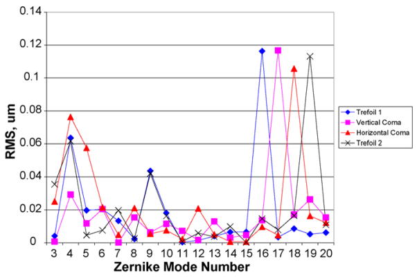
While the RMS error for most of the mode shapes appears to be distributed somewhat randomly over a variety of spatial frequencies, the four third order modes show distinctive coupling to their fifth order counterparts. This fact is illustrated in Fig. 7, which shows the RMS error for these four modes (Trefoil 1, Horizontal Coma, Vertical Coma, and Trefoil 2) decomposed using the first 20 Zernike coefficients. In the figure, the Zernike polynomials are numbered sequentially, using the single-index notation from Malacara [18]. The figure shows that the RMS error for each third order mode is mainly due to a strong component of the corresponding fifth order mode (i.e. the RMS error of Trefoil 1, , is mainly contributed by Secondary Trefoil 1, ). No similar coupling was observed between second and fourth order modes, where the RMS errors were distributed roughly randomly between the various Zernike modes.
Fig. 7.
RMS error for four of the mode shapes decomposed using the first 20 Zernike coefficients.
3.3. Dynamic characterization
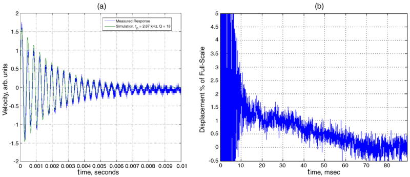
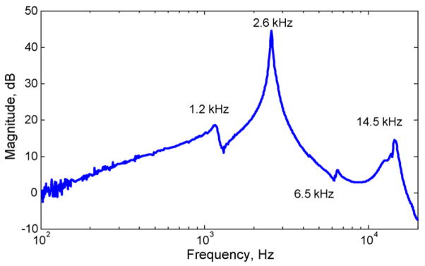
The dynamic characteristics of two DMs were measured experimentally. Initial measurements were obtained using a laser Doppler vibrometer (LDV, Polytec OFV-512). Frequency response measurements were obtained using a dynamic signal analyzer (Stanford Research Systems SR780) which was coupled to the front-face electrode of the DM through a high voltage amplifier (Piezo Systems EPA-104–115). The velocity and displacement of the mirror surface in response to a step voltage input are shown in Fig. 8. The initial settling behavior is dominated by a lightly damped mode at approximately 2.6 kHz. After the initial 10 ms settling time, a slow creep of approximately 1% of the full-scale displacement was observed over a 60 ms interval. In addition to the dominant mode at 2.6 kHz, the DM frequency response contains three other modes below 20 kHz, as shown in Fig. 9.
Fig. 8.
Step response measurements. The initial response is accurately described by an underdamped second order model with fn = 2.67 kHz and Q = 18 (a). Following the initial 10 ms transient response, the DM displays a slow creep of 1% of full-scale displacement over the next 60 ms (b).
Fig. 9.
DM frequency response measured with the LDV.
In order to identify the mode shapes associated with each natural frequency, the stroboscopic interferometer was used to record the surface deformation of a second DM in response to step changes in the voltage applied to the back face electrodes. The voltage on all the back face electrodes was initially set to 0 V, causing the mirror to assume a parabolic shape. The voltage on the back face electrodes was then set to the voltage required to flatten the DM surface, producing a step disturbance to the mirror. Surface height measurements, w(r, θ, t), were recorded every 10 μs over a 1 ms interval, for a total of 100 surface measurements. After removing the tilt from each surface, the resulting data set was analyzed by fitting each surface profile measurement with the first four mode shapes defined by (8) using a least-squares fitting algorithm. Mathematically, this can be expressed as
| (14) |
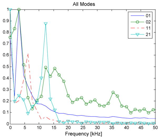
where mn = 01, 11, 21, 02, and e(r, θ, t), represents the residual error after the least-squares fit. The frequency content of each mode shape was then identified by computing the FFT of the amplitude coefficients, Amn(t). The magnitude of the FFT of each of these coefficients is displayed in Fig. 10. The dominant frequency component of each amplitude coefficient is summarized in Table 2 along with the natural frequencies measured with the LDV and with the theoretical values predicted from the solution of (9) and (13). The coefficient for the 02 mode shape, A02, appears to contain components from the 01 and 21 modes. We attribute this to the fact that the surface profile measurements obtained with the interferometer only capture the center 10 mm of the DM, making it difficult to entirely resolve the difference between the various mode shapes. In addition, the interferometer is incapable of resolving the rigid-body mode, since the analysis software only accounts for relative difference in the height across the DM, rather than rigid-body translation of the entire DM. The LDV measurements did not capture the 21 mode, suggesting that the LDV measurement beam may have been located on a node for this mode.
Fig. 10.
FFT magnitude of measured modal amplitude coefficients.
Table 2.
Modal frequencies
| Mode | Model (kHz) | LDV (kHz) | Interferometer (kHz) |
|---|---|---|---|
| Rigid body | 1.1 | 1.15 | – |
| 01 | 2.8 | 2.6 | 3 |
| 11 | 6.7 | 6.5 | 6.2 |
| 21 | 11.3 | – | 12.3 |
| 02 | 13.1 | 14.5 | 15.4 |
4. Conclusion
As expected for a bimorph DM, the AOptix device is capable of generating large displacements at low spatial frequencies. At a constant front-face voltage of 100 V, the measured peak-to-valley surface displacement was approximately ±8 μm for the second order aberrations of defocus and astigmatism, corresponding to a defocus of ±1.2 Diopters over the 10.2 mm DM pupil. For comparison, this is four times the range of defocus and eight times the range of astigmatism recently reported by Fernandez for the OKO DM [22]. In addition, by varying the potential of the front-face electrode, the AOptix device can generate an even larger range of ±3 Diopters of defocus. Although the maximum deformation that the DM can generate diminishes approximately with the square of the mode’s radial order, we were able to generate fifth order modes with 1–1.5 μm of peak-to-valley deformation. Because this range of deformations is comparable to that expected from the 2 μm stroke Boston Micro-machines DM, it is expected that both DM’s will display similar capabilities for correcting aberrations up to the fifth radial order. The transient response of the DM is dominated by a 2.6 kHz mode. Although the lowest natural frequency of this mirror was measured to be 1.1 kHz, we attribute this to a rigid-body mode of the DM. Since the DM and wavefront sensors are located at conjugate planes in a typical AO system, the rigid body mode is unlikely to have a measurable impact on the closed-loop performance of the DM. The remaining measured natural frequencies are within 15% of the predictions of a model based on classical plate theory.
Acknowledgments
The authors acknowledge the help of Steven M. Jones from Lawrence Livermore National Laboratory. SPL and JSW are supported by the National Eye Institute (Grant EY 014743).
Biographies
David Horsley received the PhD degree in Mechanical Engineering from the University of California at Berkeley in 1998. In 1998 he developed a MEMS-based fiber-optic variable attenuator for Dicon Fiberoptics. From 1999 to 2000, he joined the Advanced Storage Department of Hewlett Packard Laboratories as part of a team of researchers developing an atomic resolution storage device. From 2000 to 2003, he was a principal engineer and engineering manager at Onix Microsystems, a start-up developing MEMS-based fiber-optic switching devices for telecommunications applications. He joined the University of California at Davis in 2003 as an Assistant Professor in the Department of Mechanical and Aeronautical Engineering. His research interests include MEMS, nanotechnology, and biosensors.
Hyunkyu Park is a Ph.D candidate in the Department of Mechanical and Aeronautical Engineering at the University of California, Davis. He received his MS in mechanical engineering in 2001 and BS in both mechanical and electrical engineering in 1999 from the Ajou University, South Korea. His doctoral research includes characterization and design of MEMS bimorph deformable mirrors for adaptive optics.
Sophie Laut is a postdoctoral researcher at the Department of Ophthalmology and Visual Science at the University of California, Davis. She holds a M. Engineering degree in Computer Science and Industrial Control System, and a Ph.D. degree in Electrical and Computer Engineering, specialization in optical processing, in 2000 from the Université de Haute-Alsace, Mulhouse (France). Her interests include adaptive optics, wave front sensors and correctors, optical information processing and diffractive optics.
John S. Werner is the Jules and Doris Stein Research to Prevent Blindness Professor in the Department of Ophthalmology & Vision Science and in the Section of Neurobiology, Physiology & Behavior at the University of California, Davis. He received his Ph.D. in Psychology from Brown University in 1979. Werner’s research is concerned with understanding structure and function of the retina, and changes associated with aging and disease. His laboratory uses adaptive optics and optical coherence tomography to image the human retina at a cellular scale.
References
- 1.Vdovin G, Sarro PM. Flexible mirror micromachined in silicon. Appl Opt. 1995;34:2968–2972. doi: 10.1364/AO.34.002968. [DOI] [PubMed] [Google Scholar]
- 2.Bifano T, Perrault J, Mali R, Hernstein M. Microelectromechanical deformable mirrors. IEEE J Sel Top Quant Electron. 1999;5:83–89. [Google Scholar]
- 3.Helmbrecht MA, Srinivasan U, Rembe C, Howe RT, Muller RS. Micromirrors for adaptive-optics arrays. Transducers the 11th Int. Conf. on Solid-State Sensors and Actuators; Munich, Germany. 2001. [Google Scholar]
- 4.Hishinuma Y, Yang E-H, Cheng J-G, Trolier-McKinstry S. Optimized design, fabrication and characterization of PZT unimorph microactuators for deformable mirrors. ASME International Mechanical Engineering Congress and Exposition; Anaheim, CA. 2004. [Google Scholar]
- 5.Porter J, Guirao A, Cox I, Williams D. Monochromatic aberrations of the human eye in a large population. J Opt Soc Am. 2001;18:497–506. doi: 10.1364/josaa.18.001793. [DOI] [PubMed] [Google Scholar]
- 6.Liang J, Williams D. Aberrations and retinal image quality of the normal human eye. J Opt Soc Am. 1997;14:2873–2883. doi: 10.1364/josaa.14.002873. [DOI] [PubMed] [Google Scholar]
- 7.Ellis E. Applied Optics. Department of Physics, University of London; 1999. Low-cost bimorph mirrors in adaptive optics, Doctoral Dissertation. [Google Scholar]
- 8.Roddier F. Adaptive Optics in Astronomy. Cambridge University Press; New York: 1999. [Google Scholar]
- 9.Horsley DA, Park HK, Laut SP, Werner JS. Proceedings of the SPIE. Vol. 5688. 2005. Characterization for vision science applications of a bimorph deformable mirror using phase-shifting interferometry; pp. 133–144. [Google Scholar]
- 10.Horsley DA, Park HK, Chuang C-W, Laut S, Werner JS. Optical characterization of a bimorph deformable mirror. ASME International Mechanical Engineering Congress and Exposition; Orlando, FL. 2005. [Google Scholar]
- 11.Zawadzi RJ, Jones SM, Olivier SS, Zhao M, Bower BA, Izatt JA, Choi S, Laut S, Werner JS. Adaptive-optics optical coherence tomography for high-resolution and high-speed 3D retinal in vivo imaging. Opt Express. 2005;13:8532–8546. doi: 10.1364/opex.13.008532. [DOI] [PMC free article] [PubMed] [Google Scholar]
- 12.Dalimier E, Dainty C. Comparative analysis of deformable mirrors for ocular adaptive optics. Opt Express. 2005;13:4275–4285. doi: 10.1364/opex.13.004275. [DOI] [PubMed] [Google Scholar]
- 13.Wang JY, Silva DE. Wave-front interpretation with Zernike polynomials. Appl Opt. 1980;19:1510–1518. doi: 10.1364/AO.19.001510. [DOI] [PubMed] [Google Scholar]
- 14.Haertling GH. Ferroelectric ceramics: history and technology. J Am Ceram Soc. 1999;82:797–818. [Google Scholar]
- 15.J.E. Graves, M.J. Northcott, Mounting Apparatus for a Deformable Mirror, US Patent 6,568,647 (2003).
- 16.Hariharan P, Oreb BF, Eiju T. Digital phase-shifting interferometry—a simple error-compensating phase calculation algorithm. Appl Opt. 1987;26:2504–2506. doi: 10.1364/AO.26.002504. [DOI] [PubMed] [Google Scholar]
- 17.Hart MR, Conant RA, Lau KY, Muller RS. Stroboscopic interferometer system for dynamic MEMS characterization. IEEE ASME J Microelectromech Syst. 2000;9:409–418. [Google Scholar]
- 18.Malacara D. Optical Shop Testing. John Wiley & Sons; New York: 1992. [Google Scholar]
- 19.Zagrai A, Donskoy D. A soft table for the natural frequencies and modal parameters of uniform circular plates with elastic edge support. J Sound Vib. 2005;287:343–351. [Google Scholar]
- 20.Puttock MJ, Thwaite TEG. Elastic compression of spheres and cylinders at point and line contact. CSIRO, National Standards Laboratory Technical Paper, 25; Melbourne, Australia. 1969. [Google Scholar]
- 21.Laut S, Jones S, Park HK, Horsley DA, Olivier S, Werner JS. Proceedings of the SPIE. Vol. 6007. 2005. Bimorph deformable mirror: an appropriate wavefront corrector for retinal imaging? pp. 142–156. [Google Scholar]
- 22.Fernandez E, Artal P. Membrane deformable mirror for adaptive optics: performance limits in visual optics. Opt Express. 2003;11:1056–1069. doi: 10.1364/oe.11.001056. [DOI] [PubMed] [Google Scholar]


