

Abstract
We introduce a new scheme of nanocontact printing that fabricates nanoarrays using stamps generated by ultraviolet nanoimprint lithography. Array patterns can be generated by this printing technique in a high-density (number of features per unit area) fashion with a feature size as low as 30 nm and period of 100 nm. Sub-500 nm alignment accuracy for multilayer printing has been obtained using a traditional contact mask aligner. We also demonstrate that we can image a nanoarray labeled by streptavidin by atomic force microscope (AFM).
I. INTRODUCTION
There is a great need for high density nanoarrays in biological fields from genomics to proteomics to drug discovery.1, 2 The development of high density nanoarray technology poses two major challenges: fabrication with high throughput and low cost, and detection with high resolution and sensitivity. In the past 15 years, many arraying technologies have been developed for making biological microarrys. Among them, photolithography is the most extensively used technique in manufacturing high density DNA microarrays.3 As far as nanoarrays are concerned, deep UV light is needed for the photolithographic fabrication. The UV irradiation may result in undesired reactions in biological molecules, such as the DNA base dimerization.4 Dip-pen nanolithography (DPN) is another attractive nano-arraying technique for writing molecules on surfaces using scanning probe tips. A 55,000 pen array has recently been demonstrated for patterning large areas with 80 million dots.5 The DPN technique may be limited to situations where scale and throughput are not of crucial importance but flexibility of design and materials choice is paramount.6 On the other hand, in order to realize the full potential of the high density nanoarrays, a sensitive detection technique should also be developed to meet the requirements of nanometer resolution and reasonable throughput. Fluorescence microscopy is the most commonly used detection method for microarrays, but the spatial resolution of conventional optical microscopy is diffraction limited to approximately one-half the wavelength of light. It has been demonstrated that scanning probe microscopy can be a useful means for high density nanoarray detection due to its sensitivity and resolution.7, 8 Here, we report a nanocontact printing based method for the fabrication of high density nanoarrays in combination with atomic force microscopy (AFM) for detection.
Nanocontact printing (nCP) is a highly-parallel, manufacturable and additive process, which transfers an “ink” from protruding areas of a stamp to the substrate surface.9 This method has been used in electronics,10–12 photonics,13 sensors,14–16 catalytic surfaces,17–19 and cell biology.20–22 However, the ability to generate dense patterns at nanoscale using nCP with accurate alignment and overlay between multiple printings has not yet been reported in literature. We have developed a new process for nCP using a stamp fabricated by UV nano-imprint lithography (UV-NIL). In the original contact printing invented by Whitesides and his conworkers, the stamp was made of soft polydimethylsiloxane,23 which is suitable only for printing microscale patterns, but not for nanoscale patterns due to the mechanical strength induced defects of the soft-PDMS.24 Since then, different stamp materials and structures have been proposed for nanoscale printing, such as hard-PDMS,25 poly(ethylene)/poly(methyl methacrylate) sheet,26 composite stamp structures with either flexible24, 27 or rigid back supports,28, 29 etc. Among them, coating a thin elastomer on a rigid back support is an attractive approach to reducing the stamp distortions for nanoscale printing with precise multilayer overlay. However, the previous work used large printing pressures (~ MPa), which could be detrimental to the nanoscale feature and stamp fidelity, and showed moderate alignment of ~ 1 μm.29 In our study, UV-NIL was exploited for low cost fabrication of the nCP stamp with a thin elastic layer (the cured UV-NIL resist) as the stamp material on a rigid back support. Printing with pressures less than one atmosphere (~ 100 kPa) has been demonstrated. A dense array was generated with a feature size of ~ 30 nm and a period of 100 nm. To the best of our knowledge, this represents the highest density with the smallest feature sizes reported to date using nCP. The alignment accuracy between multilayer printings was less than 500 nm, which is the limit of the conventional contact mask aligner. We have used the stamps to produce biotin nanoarrays and detected the arrays by streptavidin labeling followed by AFM imaging.
II. EXPERIMENT AND RESULTS
Figure 1 shows the schematics of fabricating nCP stamps using a two-step UV-NIL replication process from a Si master. The Si master was fabricated with pillar array patterns of feature sizes between sub-50 nm to 10 μm and heights between 60 to 160 nm by electron beam lithography of poly(methyl methacrylate) (PMMA 950K) resist, electron beam evaporation of Cr, lift off and fluorine-based dry etching of Si. Then, it was used to generate a negative stamp by the UV-NIL replication. The negative stamp was used in a second UV-NIL replication process to generate an nCP stamp with the same kind of features as those on the Si master. This process does not require any additional pattern transfer and can produce nCP stamps rapidly with low cost.30 The choice of a two-step replication process is due to the ease of fabrication of a positive Si master using electron beam lithography. It also has the advantage of extending the lifetime of the Si master, which is costly to make. One-step UV-NIL can also be used, provided a negative Si master. To fabricate both negative and nCP stamps, UV-NIL resist (NXR-2010 from Nanonex, Monmouth Junction, NJ) of 100–200 nm was spun on a glass or quartz substrate with a thickness of 150 μm to 1 mm. The substrates were cleaned with the RCA solution (NH4OH:H2O2:H2O = 1:1:5) at 75 °C before spin coating to improve the adhesion between the substrate and the resist. UV-NIL and the first layer nCP processes were conducted using either a home made press chamber with air cushion press technology,31 or a HTG 3000HR contact mask aligner. The resist was cured using a 400 watt UV lamp with a dose greater than 40 mJ/cm2. The second layer nCP for alignment was carried out using the mask aligner. A fluoroalkyltrichlorosilane release agent is applied to both the Si master and the negative stamp surfaces for better mold release in UV-NIL. A silicon master can be used over years to generate hundreds of nCP stamps without physical degradation. We observed that the feature size on the nCP stamp was smaller than that on the Si master. We attribute this to the densification of the UV resist during curing. This feature size shrinkage is dependent on the size and shape of the pattern and the resist properties,32 and becomes more complicated in our experiments due to the two-step replication process. Its detailed study is not in the scope of this work and will be studied elsewhere. The shrinkage in thickness of a uniform UV resist in our experiments was measured to be 11% by ellipsometer, typical for an acrylate-based UV resist.32 We did not observe any detrimental effects of the shrinkage on single layer nanocontact printing and single point alignment. We expect adverse effects of the resist shrinkage in future large area overlay experiments. To minimize the shrinkage effect, a UV resist with less densification during curing can be used.33 Single step UV-NIL replication could also reduce the resist shrinkage effect.
Figure 1.

Schematics of fabricating nCP stamps by a two-step UV-NIL replication process from a Si master.
To test the nCP stamps for printing nanoarrays a gold-gold cold welding34 transfer was carried out. This technique was chosen because the nanopatterns can be easily inspected by a high resolution scanning electron microscope (SEM) and there is no complication of ink diffusion on the substrate. First, a gold ink film with 8–12 nm thickness was evaporated on the stamp by electron beam with a flux perpendicular to the stamp surface, and then it was printed on a Si substrate coated with 2 nm of chromium and 5–8.5 nm of gold. The printed arrays were inspected by a Hitachi S4700 field emission SEM, which showed good pattern transfer with a feature size down to 30 nm. Figure 2 shows both large view and zoomed-in SEM images of the nCP stamp and a printed gold array of 30/100 nm (feature size/period). It can be seen that the printed gold dots have the same size as those on the stamp with a variation of less than 5 nm, showing high resolution of the printing. The shape of the printed gold dots, however, deviates from the round shape of the dots on the stamp. We attribute this to the grain formation process during gold inking by evaporation,35, 36 and the possibility of gold deposition on the sidewalls of the stamp features.36
Figure 2.
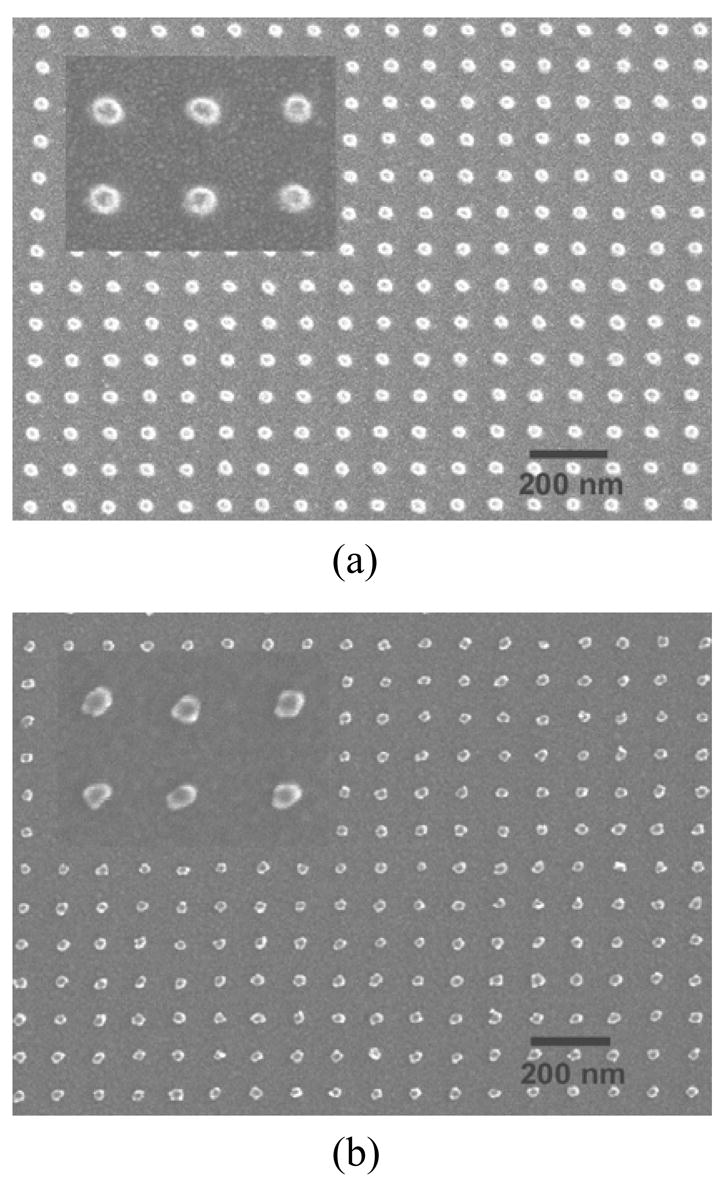
SEM images of a 30/100 nm array by nCP: a) the nCP stamp; b) the cold welding printed gold nanoarray.
The nCP stamps can operate at low pressure and have shown low distortion. For contact printings on a rigid substrate using a rigid stamp coated with a thin elastomer (200 nm or less in our case), a high printing pressure is usually required to bend the stamp and substrate in order to create a conformal contact. The contact pressure however can remain very low if the stamp and substrate surfaces are flat and parallel enough. Indeed, we have demonstrated that less than atmospheric pressure is needed after carefully maintaining the surface flatness. However, to ensure good printing, a 136 kPa printing pressure was generally used in our current research-laboratory fabrication environment (class 1000 cleanroom) due to many factors that can cause the surface to be non-flat, such as particles and resist thickness variation at the sample edge. The thickness of a rigid support plays an important role in printing pressure because the bending energy of a rigid material increases dramatically with thickness. The rigid supports in our nCP stamps were 500 μm thick or less. In addition to printing at low pressures, the nCP stamp does not show any significant distortion when printing at high pressures. Figure 3a shows an optical image of a single square cell of a gold grid pattern printed by gold-gold cold welding using a stamp with a 150 μm thick rigid support at a 340 kPa printing pressure. Each grid line consists of two 3 μm wide lines that are 2 μm apart (difficult to distinguish due to the magnification of the image). The adjacent grid lines are 500 μm apart from center to center and the relief height of the stamp was only 60 nm. No gold film was printed inside the 500 μm square grid cell except the cell label pattern at the bottom of the cell (which is also on the stamp), indicating no collapsing of the stamp during printing. We attribute this to the structure of our stamp and the relatively large modulus (~ MPa32) of UV cured elastomers.
Figure 3.

a) Optical image showing no stamp collapsing during gold-gold cold welding nCP for a stamp relief height of only 60 nm over 500 μm distance; b) box and cross patterns showing X and Y misalignments by nCP (115 nm and 162 nm respectively) are both less than 500 nm; the bar is 500 nm.
Alignment and overlay is another important aspect of nCP. To demonstrate the alignment capability, we carried out the gold-gold cold welding nCP process on a HTG HR3000 mask aligner with a custom built stamp holder that can apply extra pressure between the stamp and substrate in addition to the atmospheric pressure generated by vacuum. Box and cross patterns of different sizes were designed for the optical alignment of nCP, as well as the characterization of the misalignment by SEM. To prepare the substrate for nCP alignment, the box patterns were etched 80 nm deep into an oxidized Si substrate by UV-NIL, dry etching using a UV-NIL resist as the etching mask and removal of the resist after etching. After coating the substrate with Cr/Au film, an nCP stamp with complimentary cross patterns was coated with gold ink, aligned to the box patterns and printed on the substrate. The alignment was done the same way as front side contact photolithography alignment using a bright field microscope on top of the stamp. The box patterns on the substrate are visible during the alignment due to the transparency of the nCP stamp and the thin thickness of the gold ink. The average alignment accuracy we obtained in multiple experiments was ~500 nm, which is the limit of the contact mask aligner we used. Figure 3b shows SEM image of the best alignment result we produced using box and cross patterns. In this result we achieved X, Y misalignments of 115 nm and 162 nm respectively, both less than 500 nm. We believe more reproducible results with better alignment accuracy can be achieved by improving the alignment stage and adopting a more sensitive alignment mechanism such as the moiré pattern technique, which has a demonstrated capability for detecting misalignments less than 10 nm.37
The nCP stamp has been further tested for printing organic molecules on the silicon dioxide surface. The silicon substrates (silicon wafer coated with 100 nm thermal SiO2) were functionalized with an amino monolayer. The surface was prepared by cleaning silicon substrates in the RCA solution at ~75°C, thoroughly rinsing them with water, and finally drying with a stream of nitrogen. The dried substrates were immersed in an ethanol solution containing 12% 3-aminopropyltriethoxysilane (APTES) for about 30 min, and then thoroughly rinsed with methanol, isopropanol, and water. The contact angle of the resultant surface is around 40 ± 5°. The thickness after APTES treatment was increased about 1.0 ± 0.2 nm, measured by an elliposometer using the same parameters as used to measure the thickness of silicon dioxide. Fluorescein and biotin nanoarrays were printed on the amine surface, respectively. Before the printing, the substrates were rinsed with 10 mM KOH to ensure that the amine group is fully deprotonated. To ink the stamp for fluorescein printing, a 2 mM solution of fluorescein isothiocyanate (FITC) in N,N-Dimethylformamide (DMF) was dispensed to spread on the stamp surface and dried in nitrogen stream for 1–2 min. Then it was printed on the substrate surface at 100–200 kPa for 5–10 min. As illustrated in Figure 4a, the fluorescein is fixed in the printed area through the reaction of isothiocyanate with amine to form a thiourea anchor. The unreacted amines were inactivated by reacting with NHS-PEO7-OMe (2mM concentration in DMF, soaking for 10 min). Figure 5a shows an image of the fluorescein arrays with different feature sizes/periods, taken under a Leica TCS NT confocal fluorescence microscope. The arrays with larger period (~ 1 μm) can be clearly distinguished with a good signal to background ratio. Those with smaller period (~ 0.5 μm) are blurred due to the limited resolution of the fluorescence microscope. To image nanoarrays with small periods, we have employed an AFM based method for readout similar to that reported by Mazzola and Fodor.8 In a similar manner as described above, a biotin nanoarray was first printed on the amine surface (Figure 4b), and then converted into a protein nanoarray by flooding the surface with streptavidin. The array was characterized by AFM scanning. Figure 5b shows a high resolution non-contact AFM image of a 50/250 nm streptavidin array. Each array feature has a uniform height of 3 nm, similar to the value reported in literature.38 It can also be seen from the AFM image that the printed feature size increased up to a value of 70 nm compared to the 50 nm feature size on the nCP stamp. We believe that it was caused by diffusion of molecules. Nevertheless, the printing fidelity can be improved by fabricating a pre-patterned substrate, in which each feature is surrounded by a passivation structure. It is well known that streptavidin specifically forms a stable complex with biotin (Kd = ~ 10−15). As a result, a biotinylated nanoarray can be characterized legitimately through the streptavidin labeling. With further development, this AFM based method may become a practical tool for imaging biological nanoarrays where the fluorescent detection is limited. All the experiments described above were carried out at room temperature, unless otherwise mentioned.
Figure 4.

A schematic illustration of chemical reactions used in fabrication of (a) fluorescein and (b) biotin nanoarrays.
Figure 5.
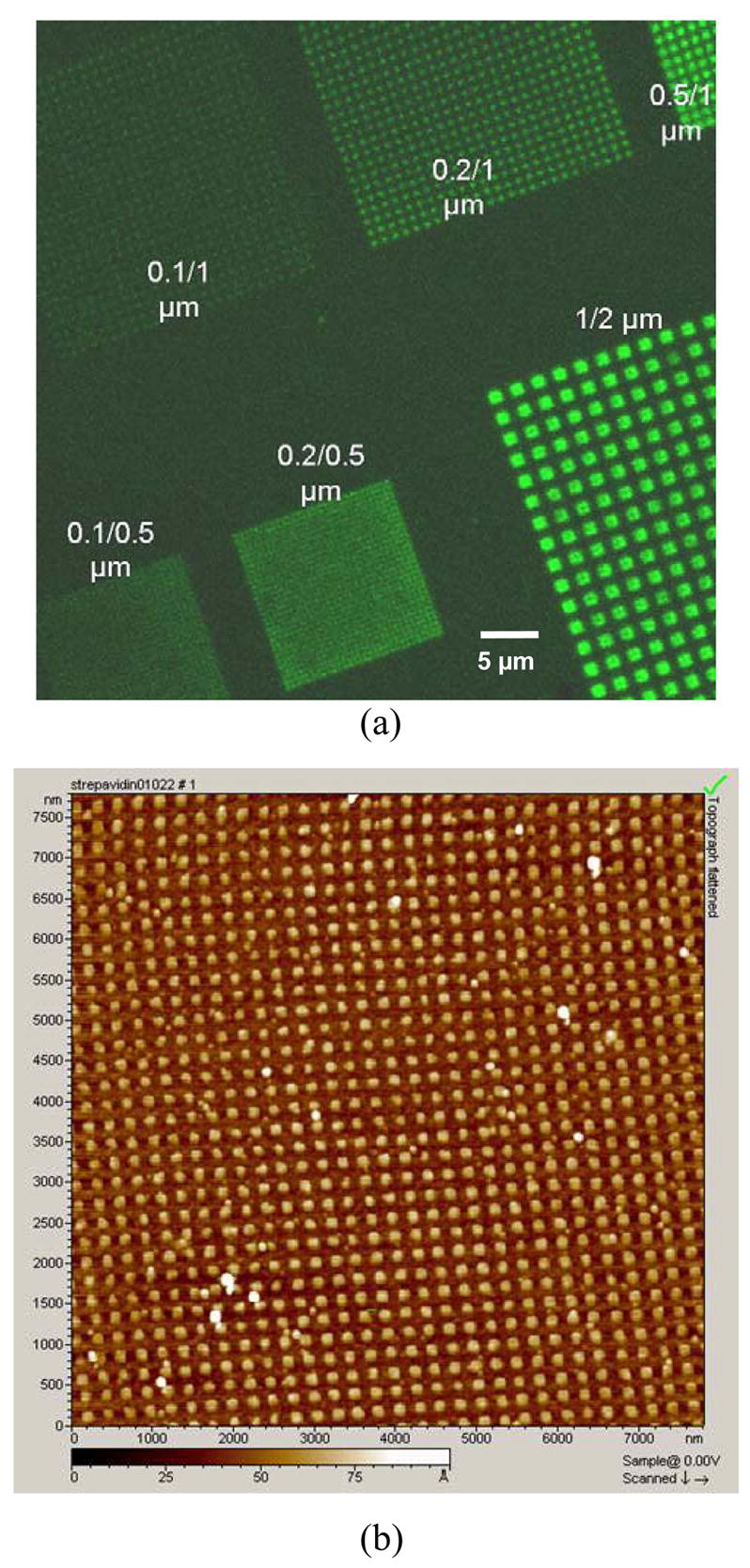
a) Confocal fluorescent image of fluorescein arrays with different feature sizes/periods; b) Topography of a 50/250 nm streptavidin array by AFM, showing a uniform height of 3 nm for each array feature.
III. SUMMARY
In summary, we have developed a method to generate high density nanoarrays using nCP. The dense nanopattern was printed down to feature sizes of 30 nm and periods of 100 nm (1×10¹⁰ features/cm2). This high density is sufficient to record an entire human genome sequence (~ 3 ×10⁹ bases) in a 1 ×1 cm chip. The printing process can be carried out at low pressures with low distortion, and readily integrated into a conventional contact mask aligner. We have achieved sub-500 nm alignment accuracy for the multilayer printing. Improvement in nanoscale alignment accuracy through further modifications of stage and alignment metrology is currently in progress.
Acknowledgments
The authors thank Prof. Stuart Lindsay for his support of the project. This work is supported by the Proposition 301 Research Funds from the State of Arizona and National Institute of Health under R21HG00415401.
References
- 1.Nicolan DV, Demers L, Ginger DS. In: Microarray Technology and Its Applications. Müller UR, Nicolau DV, editors. Springer. 2005. pp. 89–118. [Google Scholar]
- 2.Wingren C, Borrebaeck CAK. Drug Discovery Today. 2007;12(1920):813–819. doi: 10.1016/j.drudis.2007.08.003. [DOI] [PubMed] [Google Scholar]
- 3.Gao X, Gulari E, Zhou X. Biopolymers. 2004;73:579–596. doi: 10.1002/bip.20005. [DOI] [PubMed] [Google Scholar]
- 4.Sinha RP, Häder DP. Photochem Photobiol Sci. 2002;1:225–236. doi: 10.1039/b201230h. [DOI] [PubMed] [Google Scholar]
- 5.Salaita K, Wang Y, Fragala J, Vega RA, Liu C, Mirkin CA. Angew Chem Int Ed. 2006;45:7220–7223. doi: 10.1002/anie.200603142. [DOI] [PubMed] [Google Scholar]
- 6.Huck WTS. Angew Chem Int Ed. 2007;46:2754–2757. doi: 10.1002/anie.200604819. [DOI] [PubMed] [Google Scholar]
- 7.SINENSKY AK, BELCHER AM. nature nanotechnology. 2007;2(10):653–659. doi: 10.1038/nnano.2007.293. [DOI] [PubMed] [Google Scholar]
- 8.Mazzola LT, Fodor SPA. Biophysical Journal. 1995;68:1653–1660. doi: 10.1016/S0006-3495(95)80394-2. [DOI] [PMC free article] [PubMed] [Google Scholar]
- 9.Xia YN, Whitesides GM. Annual Review of Materials Science. 1998;28:153–184. [Google Scholar]
- 10.Briseno AL, Mannsfeld SCB, Ling MM, Liu SH, Tseng RJ, Reese C, Roberts ME, Yang Y, Wudl F, Bao ZN. Nature. 2006;444(7121):913–917. doi: 10.1038/nature05427. [DOI] [PubMed] [Google Scholar]
- 11.Loo YL, Lang DV, Rogers JA, Hsu JWP. Nano Letters. 2003;3(7):913–917. [Google Scholar]
- 12.Rogers JA, Bao Z, Baldwin K, Dodabalapur A, Crone B, Raju VR, Kuck V, Katz H, Amundson K, Ewing J, Drzaic P. Proceedings of the National Academy of Sciences of the United States of America. 2001;98(9):4835–4840. doi: 10.1073/pnas.091588098. [DOI] [PMC free article] [PubMed] [Google Scholar]
- 13.Lee TW, Zaumseil J, Bao ZN, Hsu JWP, Rogers JA. Proceedings of the National Academy of Sciences of the United States of America. 2004;101(2):429–433. doi: 10.1073/pnas.0304179101. [DOI] [PMC free article] [PubMed] [Google Scholar]
- 14.Basabe-Desmonts L, Beld J, Zimmerman RS, Hernando J, Mela P, Parajo MFG, van Hulst NF, van den Berg A, Reinhoudt DN, Crego-Calama M. Journal of the American Chemical Society. 2004;126(23):7293–7299. doi: 10.1021/ja049901o. [DOI] [PubMed] [Google Scholar]
- 15.Renault JP, Bernard A, Juncker D, Michel B, Bosshard HR, Delamarche E. Angewandte Chemie-International Edition. 2002;41(13):2320–2323. doi: 10.1002/1521-3773(20020703)41:13<2320::AID-ANIE2320>3.0.CO;2-Z. [DOI] [PubMed] [Google Scholar]
- 16.Xiao PF, He NY, Liu ZC, He QG, Sun X, Lu ZH. Nanotechnology. 2002;13(6):756–762. [Google Scholar]
- 17.Hidber PC, Helbig W, Kim E, Whitesides GM. Langmuir. 1996;12(5):1375–1380. [Google Scholar]
- 18.Wilhelm T, Wittstock G. Langmuir. 2002;(24):9485–9493. [Google Scholar]
- 19.Delamarche E, Donzel C, Kamounah FS, Wolf H, Geissler M, Stutz R, Schmidt-Winkel P, Michel B, Mathieu HJ, Schaumburg K. Langmuir. 2003;19(21):8749–8758. [Google Scholar]
- 20.Chen CS, Mrksich M, Huang S, Whitesides GM, Ingber DE. Science. 1997;276(5317):1425–1428. doi: 10.1126/science.276.5317.1425. [DOI] [PubMed] [Google Scholar]
- 21.Mrksich M, Dike LE, Tien J, Ingber DE, Whitesides GM. Experimental Cell Research. 1997;235(2):305–313. doi: 10.1006/excr.1997.3668. [DOI] [PubMed] [Google Scholar]
- 22.Park TH, Shuler ML. Biotechnology Progress. 2003;19(2):243–253. doi: 10.1021/bp020143k. [DOI] [PubMed] [Google Scholar]
- 23.Kumar A, Whitesides GM. Applied Physics Letters. 1993;63(14):2002–2004. [Google Scholar]
- 24.Odom TW, Love JC, Wolfe DB, Paul KE, Whitesides GM. Langmuir. 2002;18(13):5314–5320. [Google Scholar]
- 25.Schmid H, Michel B. Macromolecules. 2000;33(8):3042–3049. [Google Scholar]
- 26.Nakamatsu K-i, Tone K, Namatsu H, Matsui S. Journal of Vacuum Science & Technology B. 2006;24(1):195–199. [Google Scholar]
- 27.Suh D, Choi SJ, Lee HH. Advanced Materials. 2005;17(12):1554–1560. [Google Scholar]
- 28.Burgin T, Choong VE, Maracas G. Langmuir. 2000;16(12):5371–5375. [Google Scholar]
- 29.Tormen M, Borzenko T, Steffen B, Schmidt G, Molenkamp LW. Applied Physics Letters. 2002;81(11):2094–2096. [Google Scholar]
- 30.Ge HX, Wu W, Li ZY, Jung GY, Olynick D, Chen YF, Liddle JA, Wang SY, Williams RS. Nano Letters. 2005;5(1):179–182. doi: 10.1021/nl048618k. [DOI] [PubMed] [Google Scholar]
- 31.Gao H, Tan H, Zhang W, Morton K, Chou SY. Nano Letters. 2006;6(11):2438–2441. doi: 10.1021/nl0615118. [DOI] [PubMed] [Google Scholar]
- 32.Colburn M, Suez I, Choi BJ, Meissl M, Bailey T, Sreenivasan SV, Ekerdt JG, Willson CG. Journal of Vacuum Science & Technology B. 2001;19(6):2685–2689. [Google Scholar]
- 33.Cheng X, Guo LJ, Fu PF. Advanced Materials. 2005;17:1419–1424. doi: 10.1002/adma.200401192. [DOI] [PubMed] [Google Scholar]
- 34.Ferguson GS, Chaudhury MK, Sigal GB, Whitesides GM. Science. 1991;253(5021):776–778. doi: 10.1126/science.253.5021.776. [DOI] [PubMed] [Google Scholar]
- 35.Schmid H, Wolf H, Allenspach R, Riel H, Karg S, Michel B, Delamarche E. Advanced Functional Materials. 2003;13(2):145–153. [Google Scholar]
- 36.Menard E, Bilhaut L, Zaumseil J, Rogers JA. Langmuir. 2004;20(16):6871–6878. doi: 10.1021/la048827k. [DOI] [PubMed] [Google Scholar]
- 37.Moel A, Moon EE, Frankel RD, Smith HI. Journal of Vacuum Science & Technology B. 1993;11(6):2191–2194. [Google Scholar]
- 38.Berquand A, Mazeran PE, Pantigny J, Proux-Delrouyre V, Laval JM, Bourdillon C. Langmuir. 2003;19:1700–1707. [Google Scholar]