Abstract
Modern Field Programmable Gate Arrays (FPGAs) are capable of performing complex discrete signal processing algorithms with clock rates well above 100MHz. This, combined with FPGA’s low expense and ease of use, make them an ideal technology for pulse timing and are a central part of our next generation of electronics for our pre-clinical PET scanner systems. To that end, our laboratory has been developing a pulse timing technique that uses pulse fitting to achieve timing resolution well below the sampling period of the analog to digital converter (ADC). While ADCs with sampling rates in excess of 400MS/s exist, we feel that using ADCs with lowing sampling rates has many advantages for positron emission tomography (PET) scanners. It is with this premise that we have started simulating timing algorithms using MATLAB in order to optimize the parameters before implementing the algorithm in Verilog. MATLAB simulations allow us to quickly investigate filter designs, ADC sampling rates and algorithms with real data before implementation in hardware. We report our results for a least squares fitting algorithm and a new version of a leading edge detector of PMT pulses.
I. INTRODUCTION
Current state of the art timing pickoff for PET systems are performed with analog constant fraction discriminators (CFDs) [1]. While CFDs can achieve sub-nanosecond timing resolution, FPGAs have made advancements in computing power and I/O sophistication that may allow them to achieve similar timing results. Many current PET systems already utilize FPGAs for data acquisition [4, 5], so it is logical to employ the already used circuit board area to compute the timing pickoff. In addition to removing the need for separate analog timing components, FPGA based timing allows many channels to be processed by a single timing circuit instead of one circuit per channel. This may facilitate the elimination of row-column summing of PMT channels, which could increase the spatial resolution of PET scanners. This approach is part of our next generation of electronics for our pre-clinical PET scanner development.
There have been previous efforts to perform the timing pickoff in the FPGA. One way is to utilize the increasing clock frequencies to perform a time-to-digital conversion [6]. This method still requires an analog comparator, and may be limited by the complexity of using fast clocks on FPGAs.
Another method is to use signal processing to achieve precisions below the sampling time interval [6]. While this method is more complex, it has the advantage of using lower frequency components. Lower frequency components are cheaper, lower power, and make circuit board design simpler.
Another constraint for our applications is keeping the operating frequency away from the proton resonance frequencies in a 3T MR scanner. Also, because clock rates in FPGAs won’t continue to dramatically increase, relying on faster clocks may not be as beneficial as relying on increasing computational ability.
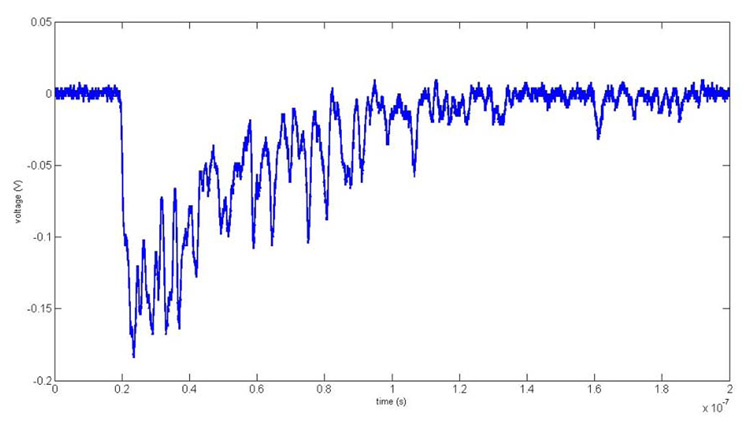
Using the known characteristics of pulses to compute the start of the pulse is one method for achieving sub-sampling timing resolution. We assume that the rise and fall times (rise refers to the first part of the pulse and fall is the second part that decays back to zero) of the PMT pulses are constants and the variability in the pulses is from the pulse amplitude and noise. The rise time is dominated by the response of the PMT while the decay time is a function of the scintillation crystal. If this assumption is true, then the start of the pulse can be determined by fitting an ideal pulse to the sampled pulse and using the ideal pulse to interpolate the starting point of the pulse. Unfortunately, the rise time of the pulse shown in Fig 1 is only a few nanoseconds long, so there is no guarantee that the ADC will sample a point on the rising edge. Without a point on the rising edge, it is impossible to distinguish curves with different amplitudes since it has a constant decay.
Fig. 1.
A representative pulse from a PMT coupled to an LSO scintillator used in this study.
II. MATERIALS AND METHODS
In order to test timing algorithms on real data, we used a 25Gs/s oscilloscope to sample 19 pulses (as shown in Fig. 1) from a PMT (Hamamatsu R5600U) that was coupled to a 2mm × 2mm × 10mm LSO crystal. A 511 KeV (22Na) source was used to generate the pulses. While the data from the oscilloscope is technically in discrete time, we feel that the sampling period of the oscilloscope (40ps) is sufficiently small enough when compared to the ADC sampling period that the scope data can be used as continuous time data. The data from the oscilloscope was then imported into MATLAB.
We have chosen to start with simulations in MATLAB for many reasons. Simulations allow the low-pass filter, ADC sampling rates and algorithms to be quickly investigated before we commit to an implementation. It also allows us to try many different fitting algorithms.
The first task was to determine the rise and fall times of the pulses. It has been previously reported in [2] that a linear rise sufficiently modeled the rise of the pulse, so we investigated ideal pulses with a linear rise and exponential decay, as well as an exponential rise and decay. To determine which pulse model was the best fit, the time constants (and line slope), and the pulse amplitude were swept until the least squared error was found for each pulse. The model that resulted in the lowest overall least squares fit was two exponentials as given by (1) where A is the amplitude and Ts is the sampling period of the ADC. Although each pulse was allowed to have a separate rise (τR) and fall times (τF), for the least squared error calculation, the average times were 310ps and 34.8ns for the rise and fall times respectively.
| (1) |
The 19 pulses were processed using these determined times. In order to trigger the oscilloscope, a threshold had to be set which introduced a time walk that was dependent on the amplitude of the captured pulse. In order to remove this bias introduced by the oscilloscope, the start times of the pulses were manually determined in MATLAB and subsequently shifted so that the start points of all pulses occurred at the same time. After the pulses are aligned, they are filtered with an ideal low-pass RC filter. The filtered pulses are then sampled to simulate an ADC of a given frequency. Each pulse is sampled with 25 different starting points to give 25 different sampled representations of each pulse. This was done to represent the free-running ADC that is asynchronous to the start of the pulses. Using the algorithms that will be presented in the next section, the starting points each of the 25 representations were interpolated. We now had 25 interpolated starting points for each of the 19 pulses that have a small distribution due to the noise still present in the filtered pulse. The interpolated starting points from one pulse were then compared to all other points from all other pulses. This was done for all pulses and a coincident timing histogram of the differences was generated. This process was done for a range of RC constants and ADC sampling values.
III. TIMING ALGORITHMS
While CFDs can achieve sub-nanosecond timing resolution [5], FPGAs have made advancements in computing power and I/O sophistication that may allow them to achieve similar timing results. There have been previous efforts to perform the timing pickoff in the FPGA. One way is to utilize the increasing clock frequencies to perform a time-to-digital conversion [6]. This method still requires an analog comparator, and may be limited by the complexity of using fast clocks on FPGAs. Another method is to use signal processing to achieve precisions below the sampling time interval [6]. While this method is more complex, it has the advantage of using lower frequency components, which are cheaper, lower power, and make printed circuit board design simpler.
Using the known characteristics of pulses to compute the start of the pulse is one method for achieving sub-sampling timing resolution. We assume that the rise and fall times (rise refers to the first part of the pulse and fall is the second part that decays back to zero, even though the “rise” on our crystals is a drop in voltage) of the PMT pulses are constants and the variability in the pulses is from the pulse amplitude and white noise. For LSO, the rise time is dominated by the response of the PMT, while the decay time is a function of the scintillation crystal. Based on these assumptions, the start time of the pulse can be determined by fitting an ideal pulse to the sampled pulse and using the ideal pulse to interpolate the starting point of the pulse.
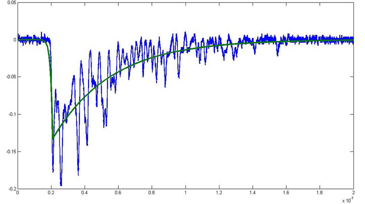
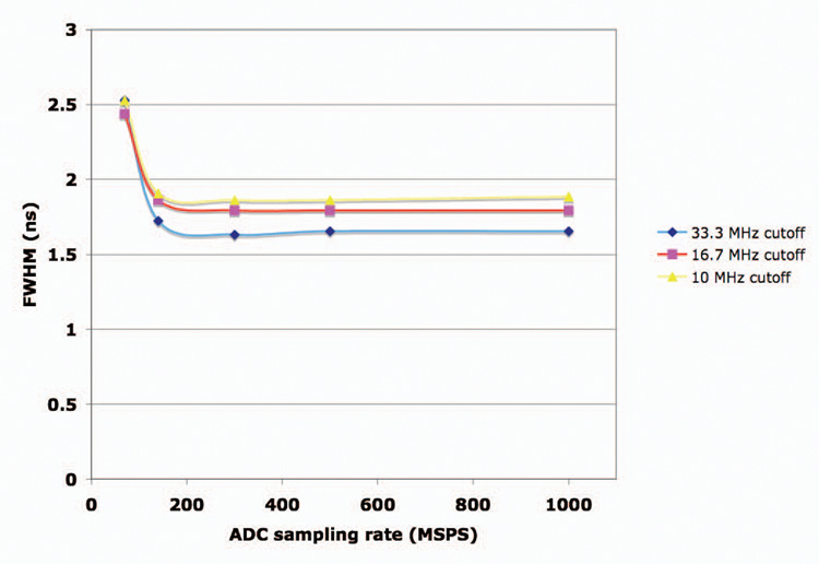
We hypothesized that if we created a pulse with two exponentials (one for the rising edge and one for the falling edge) and found the amplitude, time shift, decaying exponential and rising exponentials that produced the best least squares fit, we could use that ideal pulse to interpolate the starting point of the pulse. Fig. 2 shows an example plot of this method. Using this “brute force” method, the full width half max of the timing pick-off is about 2.5ns with a 70MHz ADC (see Fig. 3). While this provides timing resolution well below the sampling rate, the search space is far too large for an FPGA to compute in real time. From the “brute force” method, we found that the rise time ranged from .1–.5ns, the decay times ranged from 28–38ns, and the amplitude ranged from .082–.185V. To cover these ranges for a reasonable time step (~40ps) would require the least squares fit to be calculated and compared at least 215,000 times for each pulse (11 decay time steps, 5 rise time steps, 11 amplitude steps and 357 time steps).
Fig. 2.
Sample pulse from a PMT coupled to an LSO scintillator, overlaid with the best least squares fit of a curve with exponential rise and fall.
Fig. 3.
Full width half max of a least square error pulse fit timing algorithm versus ADC sampling rates.
Obviously, we must make some compromises to create an efficient FPGA-based algorithm. The first compromise was to use one rise and fall time constant. The rise and decay times that gave the best overall least squares fit for all unfiltered, unsampled data were 310ps and 34.5ns. With fixed rise and fall times, the “brute force” method timing resolution degrades by 10%. However, even after eliminating the time constant searches, almost 4,000 searches would still be required for each event.
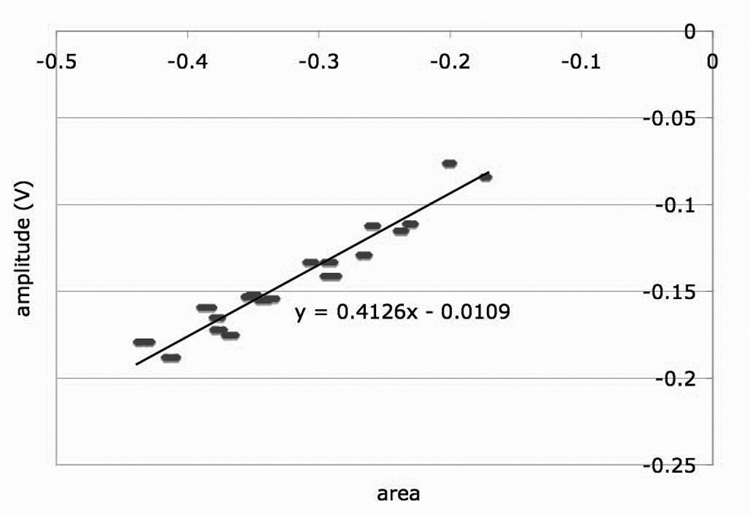
To eliminate the search for amplitude, we discovered that there is a direct correlation between the area and amplitude of the pulse, as shown in Fig. 4. The function to convert area to amplitude was determined by sampling each of the 19 pulses with many different starting points, and correlating the area obtained for each sampling to the known amplitude for that complete pulse. Using this estimation, the timing resolution is degraded by 20%.
Fig. 4.
Plot of the area of sampled and filtered pulses versus the amplitude of the pulses. The best linear fit is used to estimate the pulse amplitude from the area of the pulse.
Most dimensions of the brute-force search have been eliminated with a loss of only 20% timing resolution, but this would still require 357 searches for each possible timing offsets. However, given that we are fitting the data to a reference curve with known rise and fall times, and normalized amplitude, we can convert the brute force search fro time to a reverse-lookup. Reverse look up refers to using the voltage to look-up table the start time of the pulse. To create this table, a reference curve is pre-calculated for each possible input voltage (for a certain bit resolution), the time it occurs from the start on the reference pulse (there will be two entries per voltage - one for the rising and one for the falling edge). Thus, each incoming voltage is can be converted to a timing offset with a simple memory operation. For an ideal pulse, the look-up of the voltage of the first sample will return how much time has elapsed from the start of the pulse to the time the first sample was taken (t0). The second sample would be Ts+ t0 and the third sample would return 2Ts+ t0 and so on. Of course noise will add an error factor to each sample. This is done for each pulse and the correct number of sampling intervals (Ts) is subtracted to normalize around t0, so that after the lookup, each of the 13 points (for 70MHz sampling rate) has a time at which it “thinks” the pulse started. If these 13 t0’s are averaged unfortunately, the timing resolution degrades significantly by 2.8x.
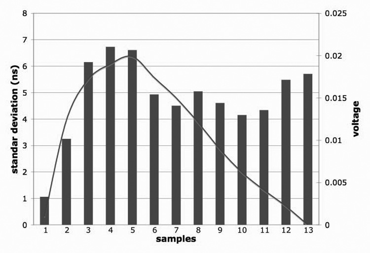
After a close inspection of the results from our look-up method, it became apparent that some of the sample points give much better results than others. This is shown in Fig. 5, which plots the standard deviation of each of the 13 samples. The standard deviation of the points was obtained by tabulating all possible samplings (at 40ps intervals) for all 19 pulses and observing the standard deviation of the inverse look up for each sample interval. For example, for sample interval 1, it is all possible samples from the start of the pulse to Ts and sample interval 2 is all points at 40ps intervals from Ts to 2Ts. Notice that the deviation is correlated with the slope of filtered pulse, and distance from the pulse start. Points at the peak (sample intervals 4 and 5) have a low slope, and thus a small change in voltage results in a large time shift. The small changes in voltages are due to the noise in the pulse. The tail of the pulse also has a large deviation. Notice also that if only the first point is used, the standard deviation is 1.03ns (FWHM 2.4ns), which essentially equals the “brute force” method.
Fig. 5.
Plot of the standard deviation of the points of a filtered pulse that is sampled with a 70MHz ADC. The line is a filtered pulse (also inverted), to give a reference for each point’s position on the pulse.
Looking at Fig 1, this makes sense since the rise of the unfiltered pulse has much less noise than the rest of the pulse. Using this information, the look-up was changed to only use the first point above .005V on the pulse. This is similar to a leading-edge detector, but automatically eliminates the effects of amplitude variation by normalizing the data to the reference pulse. It also has better noise immunity; since it can test very close to the signal start (where results are most accurate), while eliminating false positives by referencing back only from strong peaks.
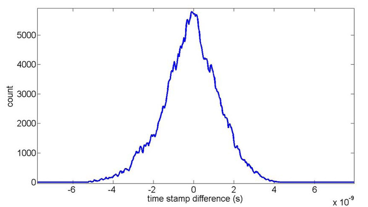
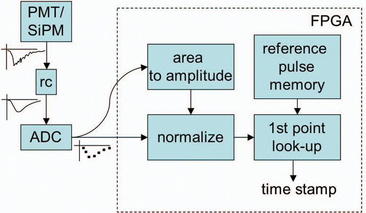
The final timing algorithm uses one decay constant, one rise constant, calculates the pulse amplitude from the area, and uses the voltage-to-time look-up for the first sample. The distribution of the final algorithm is shown in Fig. 6 for a 70MHz ADC. The architecture of our final timing algorithm is shown in Fig. 7.
Fig. 6.
The distribution of difference of time stamps between two pulses for a sampling rate of 70MHz.
Fig. 7.
The architecture of the timing pick-off circuit implemented in the FPGA.
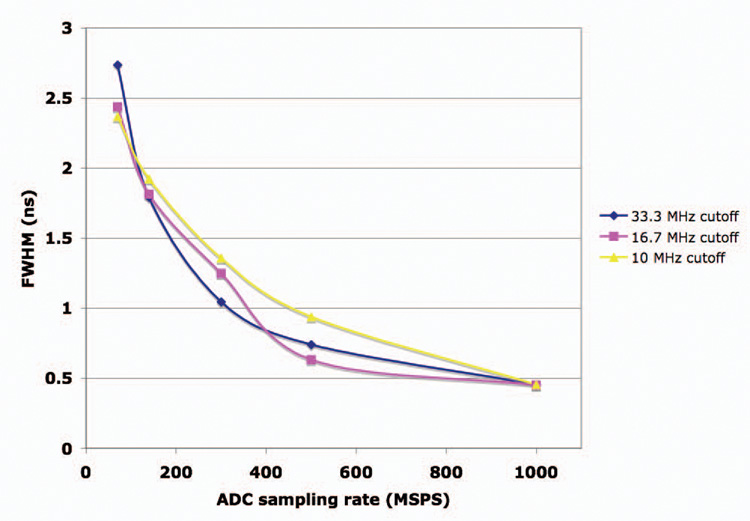
With our method, we have FWHM of 2.4ns using a 70MHz ADC and a 10MHz cutoff low-pass filter, as compared to 390ps for a simulated CFD on the same data. While our current design with a 70MHz ADC has a lower timing resolution than an analog CFD, Fig. 8 shows that as ADC technologies improve, the timing resolution will improve. Given that the resolution of a CFD does not scale with technology (CFD performance has remained fairly constant over the last decade or more), our algorithm may outperform the CFD with a 500MHz ADC (available now in parallel ADCs, and expected soon in serial ADCs). Note that even in situations where our technique does not match CFDs in timing resolution, CFDs require per-channel custom logic, in fixed ASICs. Our all-digital processing avoids this cost, which is substantial in future PET scanners with hundreds of channels per FPGA.
Fig. 8.
Plot of the full width half max coincidental timing resolution of our timing pick-off algorithm simulation.
IV. DISCUSSION
The initial simulation results indicate that we will be able to achieve timing pickoff precision well below the sampling rate of the ADC. While pulse fitting with least square error produces good timing resolution, the precision won’t get better as ADC sampling rates increase above 200MSPS. It is also too computationally expensive to compute in real time. By eliminating the search aspect of the fitting algorithm, we were able to create a timing pick-off algorithm that is well suited to FPGAs. The timing algorithm also achieves good timing results that will continue to improve as ADC sampling rates increase with technology advances.
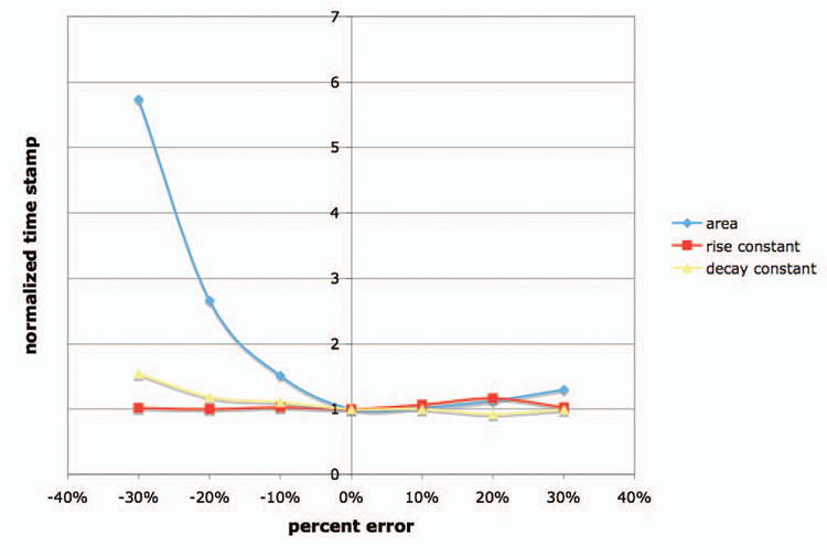
As we begin to implement this algorithm in the FPGA, there will be some issues that affect the final timing resolution. Of course there will be additional noise introduced by real ADCs and low-pass filters, but there will also be some tuning needed. Specifically, our algorithm requires a representative pulse with a rise and decay time to built. It also requires a conversion from pulse area to amplitude to be calibrated. As a part of FPGA implementation, we will implement a calibration technique, but Fig. 9 shows that we don’t have to be exact in the parameters. As long as we are in the range of 0–10% error for each parameter, the resolution will only suffer less than 10%. The quick rise in normalized time-stamp distribution for underestimating the pulse amplitude is because as the pulse amplitude is lower, the amount of the rising edge that the first sampling interval cover increases. As Fig. 5 shows, the farther the samples are up the rising edge, the larger the distribution is.
Fig. 9.
Plot of the susceptibility of our timing algorithm to the correct amplitude (area), rise and decay constants. The time stamps are normalized to the parameters found by a least squared error which are represented by 0% error.
V. CONCLUSION
We have developed a novel timing pick-off algorithm for placing time stamps on scintillation events for PET. Our timing algorithm achieve timing resolution well below the ADC sampling rate and will continue to improve as ADC technology advances. While we are still working on an FPGA implementation, we have shown that an implementation will not be oversensitive to real system parameters.
Acknowledgments
This work was supported in part by Zecotech, Altera, and NIH grant EB002117.
Contributor Information
Michael D. Haselman, Email: haselman@ee.washington.edu, Dept. of Electrical Engineering, University of Washington, Seattle, WA 98195 USA.
Scott Hauck, Dept. of Electrical Engineering, University of Washington, Seattle, WA 98195 USA.
Thomas K. Lewellen, Dept. of Radiology, University of Washington, Seattle, WA 98195 USA..
Robert S. Miyaoka, Dept. of Radiology, University of Washington, Seattle, WA 98195 USA..
REFERENCES
- 1.Moses WW, Ullish M. Factors Influencing Timing Resolution in a Commercial LSO PET Scanner. IEEE Trans. Nuclear Science. 2006;vol. 43(no 1):78–85. [Google Scholar]
- 2.Zhang N, et al. A Pulse Shape Restore Method for Event Localization in PET Scintillation Detection; IEEE Nuclear Science Symp. Conf. Record; 2004. pp. 4084–4088. [Google Scholar]
- 3.Leroux J-D, et al. Time Discrimination Techniques using Artificial Neural Networks for Positron Emission Tomography; IEEE Nuclear Science Symp. Conf. Record; 2004. pp. 2301–2305. [Google Scholar]
- 4.Laymon CM, et al. Simplified FPGA-Based Data Acquisition System for PET. IEEE Trans. Nuclear Science. 2003;vol. 50(no 5):1483–1486. [Google Scholar]
- 5.Imrek J, et al. Development of an FPGA-Based Data Acquisition Module for Small Animal PET. IEEE Trans. Nuclear Science. 2006;vol. 53(no 5):2698–2703. [Google Scholar]
- 6.Fries MD, Williams JJ. High-Precision TDC in an FPGA using a 192-MHz Quadrature Clock; IEEE Nuclear Science Symp. Conf. Record; 2002. pp. 580–584. [Google Scholar]


