

Abstract
Our laboratory has been developing a depth-of-interaction (DOI) detector design based on light sharing between pairs or quadlets of crystals. Work to date has been utilizing 2×2 mm cross section crystals carefully positioned on a multi-anode PMT. However, there is still significant light sharing in the PMT glass envelope and current PMT designs do not allow one-on-one coupling for arrays of smaller cross section crystals. One-on-one coupling is optimal for implementing the DOI estimator. An alternative to PMTs is to take advantage of progress in fabrication of metal resistive-layer semiconductor photodetectors to provide arrays with one-on-one crystal coupling. We report on our initial tests of one manufacturer's devices. The photodetector (MAPD) and scintillator combination (LFS-3) are both products of Zecotek. The LFS-3 crystal is a variant of LFS that has a better spectral match to the MAPD. Measurements show performance equivalent to or better than that obtained with PMTs and LSO, LFS, or LYSO crystals. For example, 2×2×20 mm crystals are providing 11% energy resolution. The high gain of such devices allow flexibility in designs for both the array and the supporting electronics. We are proceeding with the dMiCE development based on the use of MAPD and LFS-3 arrays.
I. Introduction
We have previously reported on a depth-of-interaction (DOI) detector design that uses light sharing and a single-ended readout scheme [1, 2]. The motivation of the initial development was to produce a cost effective DOI system that could be adapted to a wide variety of crystal types since it did not rely on mixing of crystals with different characteristics such as is done in techniques using pulse shape discrimination. The use of a single ended light readout should result in a cost effective system in that the number of photoreceptors and associated electronic channels are minimized. Finally, a single ended approach also simplifies construction in terms of not having to accommodate signal paths and support of active devices on both sides of the crystal arrays.
While our initial work has been promising, practical implementation for small cross section crystals and optimization of the light sharing has been limited due to our initial use of PMTs. We face problems with controlling light sharing due to the glass envelope of the PMT and the cost of multi-anode PMTs even when the anode pitch is adequate to allow one-on-one coupling. Our initial approach was to attempt to develop an estimator that could deal with sharing of crystal pairs with a coarse anode pitch (a many on one coupling problem). While that is still ongoing, our preferred approach is a one-on-one coupling scheme.
The basic design, termed dMiCE, builds upon our earlier work on the micro-crystal element detector module (MiCE). The approach for DOI data extraction is shown in Figure 1. The light sharing along the long length of a pair of crystals is used to create a DOI dependence on the ratio of the light outputs from the crystals [A/(A+B)]. The approach we have used is to allow no sharing near the photodetector and full sharing near the front of the crystals (as shown in Figure 1). For our initial work, we have utilized a multi-cathode photomultiplier (PMT) so that each crystal is directly coupled to a single photocathode, but there is still significant light sharing in the glass envelope of the PMT. In our new methods we plan to investigate controlling light sharing through painted reflectors and laser cut patterns of 3M polymer reflective film (the same material we used in our MiCE2 detector design) [3-5].
Figure 1.

dMiCE detector concept. (a) DOI detector unit. (b) PMT ratio plots [A/(A+B)]. A significant amount of light is shared when an event is detected near the entrance face of the detector unit. Less sharing occurs for interactions near the PMT interface
A complication in any DOI design is that about half the time, the interaction of the primary gamma ray in the detector will be a Compton scattering event. If the crystals are sufficiently long, the scattered gamma ray will then undergo more interactions, often ending with a photoelectric absorption. To achieve good sensitivity, we often want to use long enough crystals to capture the scattered gamma ray - resulting in more than one point of light generation in the detector block (Figure 2). Thus, a challenge in any DOI development is how to handle scattered events within the block. Approaches that have been developed by many groups include a correction for the basic detector response in the reconstruction algorithm, and development of statistical position estimators that take such scattered events into account. For our first pre-clincal scanner (MiCES), we implemented a version of OSEM that included our system's detector response [6]. We are currently working on a statistical estimator to determine the point of first interaction in our dMiCE designs. However, we can gain some additional information to address this problem by using one-on-one coupling as diagrammed in Figure 2.
Figure 2.
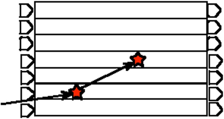
Diagram of the multiple light sources within a detector array due to scatter. The design shown here is for a double sided one-on-one scheme. The main dMiCE design uses only a single ended one-on-one crystal to detector scheme.
One of the alternative approaches to DOI determination developed by several different groups is to place photo detectors at both ends of a stack of crystals and measure the light ratio from the detectors at each end to determine DOI. Most of the work to date has been done with a many crystal to one coupling scheme with devices such as position sensitive avalanche photodiodes (PSAPD).
With the development of metal resistive-layer semiconductor photodetectors (or Geiger-Muller mode avalanche photodiodes - GMAPD) we now have a photo sensor that has the potential of providing us with a cost effective one-on-one coupling capability with fine pitched crystal arrays. We are currently using MAPDs, prototype versions of GMAPDs fabricated by Zecotek, in our dMiCE development. Figure 3 depicts 1×2 and 2×2 prototype arrays as well as an image of a pair of 2×2 mm cross section crystals mounted to one of the 1×2 arrays.
Figure 3.

Prototype Zecotek Type 3 MAPD arrays. Left are examples of the 1×2 and a 2×2 arrays. Right is a 1×2 array coupled to a pair of LFS-3 crystals.
On advantage of using a device such as a fine pitched MAPD array is the ability to provide a discrete photodetector for each crystal element (Figure 2). One can then either place the MAPD array on one side as for our dMiCE concept or both sides similar to what others have done with PSAPDs. By going to one-on-one coupling, one has the advantage of generating a DOI value for each of the interaction sites within the array - allowing a much easier task for an estimator to determine the point of first interaction. One of the challenges in implementing the one-on-one schemes is the number of electronic channels needed. For example, if we use a 20×20 array of crystals and implement a dual sided photon detector scheme with discrete processing of each detector, we would have to deal with 800 channels of data per module (many thousands of channels for a scanner). One obvious approach to reduce the number of channels is to implement a row-column summing approach, which reduces the number of channels per module to 80 for the dual side approach and 40 for our dMiCE approach. Our current focus is on implementing our dMiCE design using one-on-one coupling with MAPD arrays and row-column summing coupled with a new electronics system based on the use of serial ADCs and performing all of the pulse processing in field programmable gate arrays (FPGA). FPGAs commonly come with built-in high speed deserializers to allow the input of data to be acquired at much higher clock speeds than those used to operate the FPGA. For example, our current design uses an Altera Stratix II device which can easily support a total of 48 channels of data from six 8 channel 70 MHz serial ADCs. Here we present some of our evaluation of MAPD devices for our dMiCE concept as well as some additional simulations of the collection of light versus interaction depth from paired crystals.
II. Material and Methods
A. MAPD and scintillator testing
Zecotek has developed three different generations of MAPDs and several different variants of their LFS crystal [7]. The characteristics of the three types of prototype MAPDs are listed in Table I. Except where noted, the data in this paper were taken with the Type 3 devices and LFS-3 crystals. Zecotek also provided us with prototype MAPD Type 3 arrays (two 1×2 devices and a 2×2 device), both using 1.1×1.1 mm2 active cells (Figure 3). Measurements of the current-voltage curves of single devices (or elements in the arrays) were performed with the circuit shown in Figure 3. Energy spectra and preliminary timing measurements of single elements utilized the circuit of Figure 4. Energy spectra from the 1×2 prototype arrays were acquired with the bias circuit of Figure 5.
Table I.
Basic parameters of three types of Zecotek prototype MAPDs.
| MAPD type |
Sensitive area (mm) |
Pixel density (pixels/mm2) |
Typical bias (VDC) |
MFR specified gain |
|---|---|---|---|---|
| 1 | 1.82×1.82 | ~950 | 81-83 | 105 |
| 2 | 1.08×1.08 | ~900 | 58-59 | 106 |
| 3 | 3.0×3.0 | ~10,000 | 136-142 | 2×10⁴ |
Figure 4.
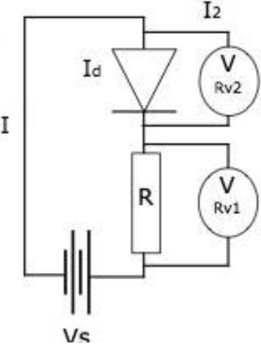
Measurement circuit for V-I curves
Figure 5.

Test circuit for the energy measurements of the individual elements of the prototype MAPD arrays.
The devices were placed in a light tight box with the bias circuit placed close to the MPAD(s) under test. The typical electronics setup is shown in Figure 6.
Figure 6.

Circuit to read out data from two elements simultaneously from a 1×2 prototype MAPD array.
B. Light sharing simulations
We have reported previously on simulations of the light sharing with shaped reflectors between the crystal pairs [1]. We are extending that work with a more careful exploration of reflector shapes and types of reflector materials. A key component is taking a closer look at the properties of those surfaces that are not shared between the crystals. DETECT [8] is being used for the light transport simulations. The specific version being used is the DETECT 2000 code which has provisions for a semiempirical model of surface roughness (UNIFIED surface). For the data presented here, we used the standard surfaces in DETECT. Specifically, we used the PAINT surface to model using white paint or TFE Teflon, and METAL for use of 3M Mirror Film. For the current series of experiments, we are using 2.2 × 2.2 mm cross-section crystals. In a similar fashion to our early work, we looked at a variety of triangle and square patterns for the reflector between the crystal pairs. We focused on triangular shapes with rectangular blocks near the MAPD (Figure 8). Combinations considered included using paint or 3M Mirror film for the shared crystal surfaces, white paint or 3M Mirror Film on the non-shared long surfaces, and combinations of black and white paint as well as 3M Mirror Film on the surface opposite the MAPD.
Figure 8.
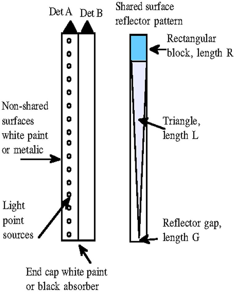
Basic geometry of simulations. Light was generated from a single point that was moved along the long axis of the crystal mounted to detector A. The shared surface between the crystals included a reflector that could consist of 3 parts (a rectangle of length R, an isosceles or right triangle of length L that stopped short of the end of the crystal leaving a “gap” of length G.
For the initial round of experiments with crystal pairs on the prototype MAPD arrays, we are using 2.2×2.2×20 mm LFS-3 crystals. The crystal are then mounted on a 1×2 array and visually positioned. With the current array pitch and the thickness of the reflector materials, the crystals were visually well centered over the array active elements.
III. Results
A. MAPD characterizations
Figure 9 depicts a typical singles energy spectrum. Figure 10 depicts a typical current-voltage curve for a Type 3 device. Figure 11 is a histogram of the gain measurements for the 2007 production LFS-3 crystals. We depict the relative gain as the MCA channel of the photopeak divided by the amplifier gain. Table II summarizes the basic measurement results. As of the submission of the conference record paper, we were unable to acquire data from the Type 2 devices. Re-coupling a given MAPD crystal pair (5 repeats) showed ~11% error. These re-coupling errors probably reflect the slightly curved optical surface of the prototype MAPDs that results in a non-uniform thickness of the coupling compound. The manufacturer assures us that the production MAPD devices will have a flat optical surface for coupling.
Figure 9.

Typical 511 kEv energy spectrum from a Type 3 MAPD device and a 2×2×12 mm LFS3 crystal. The energy resolution is 11%.
Figure 10.

Typical current-voltage curve for a MAPD type 3 device.
Figure 11.

Histogram of the relative gains of a Type 3 MAPD with different samples of 2007 production LFS-3 crystals (2×2×12 and 2.2×2.2×20 mm3) with a 500 ns amplifier shaping time.
Table II.
Repeated test results of MAPD
| Parameter | Type 1 MAPD |
Type 3 MAPD |
R2548 PMT (900 VDC) |
|---|---|---|---|
| Relative gain, 250 ns shaping | 3.9 | 1.7 | 1.4 |
| Energy resolution, 250 ns shaping |
14.6% | 11% | 14% |
We have done preliminary time resolution measurements, but at the time of submission of this paper, Zecotek was working on improvements in the MAPD design that impacts timing. Early tests by the manufacturer on the next version of the Type 3 MAPD devices coupled to LFS-3 crystals obtained a coincidence timing resolution of 750 ps. Since further improvements in timing are expected during the Fall of 2007 (improved linearity, improved timing, improved packaging), we did not pursue more timing tests with the samples used for the data in this paper.
B. Paired crystal simulations
A wide variety of reflector combinations were investigated. The best performance for the shared interface reflector was obtained with the basic geometry of Figure 8 using an isosceles triangle with a metallic reflector on the unshared surfaces. In general, we found the use of the metallic reflector on the unshared long surfaces was significantly better than a white reflector. Figure 12 is a plot of detector A and B response versus point source depth (from the detector surface) in detector A for an isosceles right triangle (the full length of the shared crystal surface), a white reflector on the unshared long surfaces, and a white reflector on the end cap (the small surface opposite from the detector). Figure 13 is the same basic geometry, but with a metallic reflector on the unshared long surfaces and a black absorber on the end cap.
Figure 12.

Plot of detector A (series 1) and detector B (series 2) as a function of depth of a point source of light from the detector. The basic geometry is shown in Figure 8. The shared reflector is an isosceles right triangle (metallic reflector), the unshared crystal sides have a white reflector, and the end cap opposite the detector is a white reflector.
Figure 13.

Plot of detector A (series 1) and detector B (series 2) as a function of depth of a point source of light from the detector. The basic geometry is shown in Figure 8. The shared reflector is an isosceles right triangle (metallic reflector), the unshared crystal sides have a metallic reflector, and the end cap opposite the detector is a black absorber.
All simulations were run ten times for each point source location to generate an estimate of the standard deviations of the detector responses. Figures 13 and 14 plot the ratios of detector B to detector A including the standard deviation results for two cases. The basic geometry for Figures 14 and 15 were the same and consisted of the same right isosceles triangle used in Figures 12 and 13. The long, unshared surfaces of the crystals were covered with a metallic reflector. The only difference is the material used on the end cap (the surface opposite the detector - Figure 8). For Figure 14 the end cap is a white reflector while Figure 15 has a black absorber. As is seen, the ratio increases with the use of the black reflector, but the resulting loss of light photons also increases the standard deviation of the measurements.
Figure 14.

Plot of the ratio of detector A (series 1) and detector B (series 2) as a function of depth of a point source of light from the detector. The basic geometry is shown in Figure 8. The shared reflector is an isosceles right triangle (metallic reflector), the unshared crystal sides have a metallic reflector, and the end cap opposite the detector is a white reflector. The “error bars” reflect the standard deviations of the data from each detector for 10 simulations at each point source location.
Figure 15.

Plot of the ratio of detector A (series 1) and detector B (series 2) as a function of depth of a point source of light from the detector. The basic geometry is shown in Figure 8. The shared reflector is an isosceles right triangle (metallic reflector), the unshared crystal sides have a metallic reflector, and the end cap opposite the detector is a black absorber. The “error bars” reflect the standard deviations of the data from each detector for 10 simulations at each point source location.
IV. Discussion
Our earlier work with our dMiCE DOI concept [1,2] was promising but limited by problems with optimization of the light sharing schemes and dealing with the decoding of the light response function if we had to resort to many-on-one coupling of the shared crystals in an array. Various position sensitive PMTs did not provide us an option for one-on-one coupling for the crystal sizes we wished to utilize for pre-clinical imaging systems. The performance we are seeing with the prototype MAPD devices has the needed energy resolution and linearity as well as adequate timing for our dMiCE detector designs. The expected improvements in the devices (e.g., improved timing resolution and MAPD arrays that will support arrays of dMiCE crystal pairs) provide us with the needed one-on-one coupling to realize construction of full dMiCE detector systems.
We have found that the design and selection of components for the bias circuits (Figures 5 and 6) is an area that needs further investigation. For example, when we attempted to use a circuit like Figure 5 to supply both elements of a 1×2 array from a common bias supply, we were unable to obtain a signal from the devices. Using the circuit in Figure 6 did allow good signals to be obtained from the array, but we do not feel that we have developed an optimal bias circuit design.
The extension of our earlier simulation work to begin looking at changes in the unshared surface treatments (Figures 12 - 15) indicates that we can trade off total light collection to improve the DOI decoding. However, the increase in variance for any individual measurement as we improve the DOI ratio parameter used in the current simulations presents us with a non-trivial optimization problem. Further, the simulation data presented here do not include Compton scattering in the crystal array. With the one-on-one coupling scheme (either single ended or dual ended - Figure 2) and small cross section crystals, a Compton scatter event followed by a photoelectric event will generally occur in different crystals. For our single-ended dMiCE design concept, small cross section crystals also mean that Compton-Photoelectric events are generally not going to occur within a single paired crystal element, but will occur between crystal pair elements (signals from four MAPD elements).
We are now taking data with crystal pairs based on the reflector designs from our simulations. In parallel, we are working on an estimation algorithm that will take into account the data from each sensor in the array and the geometry of the scanner to determine the point of first interaction within the detector array. That algorithm will need to take into account: 1) the fact that the total amount of light extracted from a crystal pair is DOI dependent; 2) the experimentally determined variance in signal for any interaction point along the long axis of a crystal pair; 3) the multiple interactions of a gamma ray within the array (e.g., Compton - Photoelectric interaction pair), and; 4) for row column summing, the impact of scattering within the detector array on the measured response functions along each row and column.
Our current development plan is to proceed with both single- and dual-ended detector designs to determine which approach provides us with the best compromise in cost and performance. The eventual cost of large arrays (e.g., 20×20 with 0.9 mm pitch) are not known at the time of submission of this summary. However, there is a great deal of effort to produce such devices at reasonable costs. In our own effort, we expect to receive MAPD arrays in the near future with much improved timing resolution and with pitches that will allow fabrication of complete arrays of various dMICE designs.
Figure 7.

Diagram of the electronics configuration for measurements of MAPD devices and prototype dMiCE detector modules.
Acknowledgments
This work was supported in part by NIH-NIBIB grants: R01 EB002117 and Zecotek. All authors are with the University of Washington Department of Radiology, Seattle, WA 98195 USA
V. References
- [1].Lewellen TK, Janes M, Miyaoka RS. Dmice - a Depth-of-Interaction Detector Design for Pet Scanners. Proceedings of the IEEE Nuclear Science Symposium and Medical Imaging Conference; Rome. 2004. pp. 2388–92. [DOI] [PMC free article] [PubMed] [Google Scholar]
- [2].Miyaoka RS, Lewellen TK, Yu H, McDaniel DL. Design of a Depth of Interaction (DOI) Pet Detector Module. IEEE Trans. Nucl. Sci. 1998;45(3):1069–73. [Google Scholar]
- [3].Miyaoka RS, Janes M, Lee KS, Park B, Kinahan PE, Lewellen TK. Development of a Prototype Micro Crystal Element Scanner (Mices): Quickpet II. Molecular Imaging. 2005:117–27. doi: 10.1162/15353500200504154. [DOI] [PubMed] [Google Scholar]
- [4].Miyaoka RS, Kohlmyer SG, Lewellen TK. A Second Generation Micro Crystal Element (Mice2) Detector. J. Nucl. Med. 2001:110P. [Google Scholar]
- [5].Miyaoka RS, Laymon CM, Janes M, Lee K, Kinahan PE, Lewellen TK. Recent Progress in the Development of a Micro Crystal Element (Mice) Pet System. Proceedings of the 2002 IEEE Nuclear Science Symposium and Medical Imaging Conference; Norfolk. 2002. pp. 1287–91. [Google Scholar]
- [6].Lee K, Kinahan PE, Fessler JA, Miyaoka RS, Janes M, Lewellen TK. Pragmatic Fully 3d Image Reconstruction for the Mices Mouse Imaging Pet Scanner. Phys Med Biol. 2004;49(19):4563–78. doi: 10.1088/0031-9155/49/19/008. [DOI] [PubMed] [Google Scholar]
- [7].Lewellen TK, Janes M, Miyaoka RS, Zerrouk F. Initial Evaluation of the Scintillator LFS for Positron Emission Tomography Applications. Proceedings of the IEEE Nuclear Science Syposium and Medical Imaging Conference; Rome: 2004. pp. 2915–18. [Google Scholar]
- [8].Moisan C, Hoskinson EM, Levin A, Vozza D. Public Domain Platform to Model Scintillation Counters for Gamma-Ray Imaging Applications. SPIE. 1997;3115:21–29. [Google Scholar]