

Abstract
This paper compares the analytical performance of microchannels fabricated in PDMS, glass, and polyester-toner for electrophoretic separations. Glass and PDMS chips were fabricated using well-established photolithographic and replica-molding procedures, respectively. PDMS channels were sealed against three different types of materials: native PDMS, plasma-oxidized PDMS, and glass. Polyester-toner chips were micromachined by a direct-printing process using an office laser printer. All microchannels were fabricated with similar dimensions according to the limitations of the direct-printing process (width/depth 150 μm/12 μm). LIF was employed for detection to rule out any losses in separation efficiency due to the detector configuration. Two fluorescent dyes, coumarin and fluorescein, were used as model analytes. Devices were evaluated for the following parameters related to electrophoretic separations: EOF, heat dissipation, injection reproducibility, separation efficiency, and adsorption to channel wall.
Keywords: EOF, Microchip electrophoresis, Separation efficiency, Substrate material
1 Introduction
Miniaturized electrophoresis devices have become a powerful analytical tool in separation science. These microdevices have many advantages over conventional CE instrumentation, including reduced sample/buffer consumption, faster analysis times, higher sample throughput, and greater separation efficiency [1, 2]. Compared with conventional CE, lower voltages are required for microchip electrophoresis due to the shorter channels that are commonly employed for the separation. This makes it possible to utilize smaller power supplies [1-3], leading to the possibility of truly portable microanalysis systems. Microchip devices have been fabricated in a wide variety of substrate materials using both standard photolithographic procedures and newer microfabrication methods [1-5].
Glass is the most popular material employed for the fabrication of microchip electrophoresis devices. This is primarily due to the similarity of the glass surface to that of fused-silica capillaries [6-8]. In addition, glass has many other positive attributes for microchip electrophoresis applications, including good mechanical and optical properties, high electrical insulation, and low chemical reactivity. Glass microchips are usually fabricated using classical photolithography combined with wet chemical etching [4-11]. Some disadvantages of glass chips are that they are expensive and relatively difficult to fabricate. Production of these chips requires access to a cleanroom and the use of corrosive etching solutions [5, 10]. In addition, the thermal bonding technique, which is often used in the fabrication of glass microchips, is time-consuming and often irreproducible.
These disadvantages related to glass microfabrication procedures have led scientists to investigate alternative materials for microchip fabrication. In particular, the production of microfluidic devices using polymeric substrates has generated significant interest due to their superior biocompatibility, greater flexibility, reduced cost, and ease of processing [12-15]. Additional advantages of polymers are that they are inexpensive, large numbers of microdevices can be fabricated from a single master, and the production of these devices does not require a cleanroom environment. These advantages make it possible for a large number of researchers to introduce microchip electrophoresis systems in their research [12-15].
A variety of polymers have been employed for microchip electrophoresis, including PMMA [16-18], poly(carbonate) [19, 20], polyethylene terephthalate (PET) [21], thermoset polyester [22, 23], polyester-toner (PT) [24-26], polyurethane [27], thermoplastic olefin polymer of amorphous structure [28], and PDMS [29-33]. Features in polymer microchips have been produced using laser ablation [34], soft lithography [27, 29-33], nanoimprint lithography [35], hot embossing [15, 20], and injection molding [36] as well as the direct-printing process [24-26, 37]. Further information about microfabrication technologies can be found in well-detailed reviews [5, 9, 12].
PDMS is the most popular polymer for microfluidic applications [15, 33]. It is elastomeric, inexpensive, possesses good optical clarity, and can also be used to construct pumps and valves [32, 38]. Another significant advantage of PDMS is its ability to generate a tight seal to itself or other flat surfaces, reversibly or irreversibly, without distortion of the microchannels. An essential element of PDMS prototyping is the fabrication of a master template. This master is commonly fabricated in photoresist (such as SU-8), silicon, or nickel [29, 32]. Disadvantages of PDMS include its hydrophobicity, which can lead to analyte adsorption, and the diffusion of non-cross-linked oligomers to the channel surface, which can lead to changes in EOF over time [29, 32]. In general, separations on PDMS microchips are inferior to those obtained on glass [39].
Of all the currently available microfabrication methods, the direct-printing process is the fastest, simplest, and least expensive means to generate microfluidic devices [24-26, 37]. This technique involves direct printing of the fluidic network onto the surface of polyester films (or overhead projection transparency films). If a laser printer (LP) is used, a thin toner layer is deposited over the polyester film with the microfluidic regions defined by white lines (channels). The printed layout is then laminated against a blank polyester film (namely, single-toner layer (STL)) or a mirror image of the layout (namely, double-toner layer (DTL)). In this case, microchannels 7±1 or 12±2 μm deep can be obtained for STL and DTL channels, respectively. Access to the microfluidic network is accomplished using holes produced in the cover polyester plate using a paper punch [24, 25, 37]. This inexpensive method has been used to fabricate PT electrophoresis microchips with successful integration of electrochemical detection modes [24-26, 40]. Toner-based techniques have also been employed to create mixers [41], laser-printed masters for the fabrication of PDMS microchannels [42-44], hybrid glass-toner [45, 46], and glass electrophoresis microdevices [47] as well as miniaturized CDtrodes employing sputtered recordable compact disks [25, 48-50] as an inexpensive gold source.
The primary goal of this manuscript is to directly compare the analytical performance of electrophoresis microchips fabricated in PT with that of those produced in more conventional substrates, including glass, native and plasma-oxidized PDMS, and hybrid PDMS/glass. PT devices have demonstrated great promise for microchip electrophoresis and present several advantages over the classical materials in terms of cost, fabrication time and, most importantly, the required instrumentation for fabrication. Therefore, a direct comparison of PT with the more classical materials is necessary so that future investigators can use that knowledge when developing a separation on this type of device. To make a fair and accurate comparison between substrates, all microchannels were fabricated with similar dimensions. Fluorescence detection was employed to rule out any losses in efficiency (band broadening) due to the detector configuration. Electrophoretic parameters such as EOF, heat dissipation, injection-to-injection repeatability, separation efficiency, and the contribution of the channel wall-to-band broadening were studied.
2 Materials and methods
2.1 Materials, samples, and reagents
The following materials and chemicals were used as supplied. Soda-lime glass wafers (5 × in.) with predeposited layers of chrome and AZ1500 photoresist were purchased from Telic (Santa Monica, CA, USA). Silicon wafers (100 mm) and Sylgard 184 were obtained from Silicon (Boise, ID, USA) and Ellsworth Adhesives (Germantown, WI, USA), respectively. SU-8 photoresist and Nano SU-8 developer were acquired from Microchem (Newton, MA, USA). AZ developer was obtained from Clariant (Sommerville, NJ, USA). Transparency films (CG 3300 model) and toner cartridge Q2612A were obtained, respectively, from 3 M (São Paulo, Brazil) and Hewlett Packard (Palo Alto, CA, USA). Diamond drill bits, dremel tool, and JB Weld epoxy-resin were purchased from Ace Hardware (Lawrence, KS, USA). The buffered oxide etchant (BOE) and chrome etchant solutions were purchased from Fox Scientific (Alvarado, TX, USA) and Cyantek (Fremont, CA, USA), respectively. Sodium hydroxide, boric acid, and sodium tetraborate were acquired from Sigma (St. Louis, MO, USA). Fluorescein (FL) disodium salt dehydrated and coumarin (CM) 519 were obtained from Eastman Kodak Fine Chemicals (Rochester, NY, USA). Sulfuric acid, 30% hydrogen peroxide, and ammonium hydroxide were purchased from Fisher Scientific (Pittsburgh, PA, USA). The 20 mmol/L boric acid/sodium tetraborate buffer solution, pH 9.0, was prepared weekly in Nanopure water (resistivity 18 MΩ cm) and filtered through 0.45 μm membrane filters before use. Stock solutions of FL and CM 519 (5 mmol/L each) were prepared daily in water and acetone, respectively. Prior to electrophoresis, sample solutions were diluted in run buffer.
2.2 Microfabrication processes
The layout of the devices was drawn using Microsoft Freehand 8.0 software. The electrophoresis microchip consisted of a simple cross-channel layout. For the production of glass and PDMS channels, the mask was printed on high-resolution transparency film by Laser Graphics (Lawrence, KS, USA). These high-resolution transparency films were used as masks in the standard photolithographic step. For PT microchips, the layout was printed directly on polyester film using an office 600-dpi-resolution LP (692 series) from Hewlett Packard. For all microfabrication processes, the mask was prepared with four similar layouts. Silicon and glass wafers were used to fabricate four devices each (glass and PDMS) while an A4 size polyester sheet allowed the printing of 12 devices (PT) at the same time.
2.2.1 Glass microchannel fabrication
Glass microchips were fabricated in-house using standard photolithographic procedures [11, 51]. The mask containing four identical layouts was placed on top of a piece of soda-lime glass (5 ± in.) with predeposited layers of chrome and AZ1500 photoresist and exposed to UV radiation for 15 s. The exposed image was developed with AZ developer for 3 min, rinsed with Nanopure water, baked at 95°C for 10 min, and placed in chrome etching solution for 2 min to remove the exposed chrome layer. The glass was then placed in a bath containing BOE solution for ca. 35 min under rigorous stirring. Once the etching of the channels was complete, the photoresist and chrome layers were removed using acetone and chrome stripper, respectively [11]. The etch profiles were measured using a Tencor Alpha Step 200 profilometer (San Jose, CA, USA).
A cover plate was prepared by drilling access holes into another piece of soda-lime glass using a 0.75-mm-diameter diamond drill bit. Prior to bonding, the cover and channel plates were chemically cleaned by immersion in piranha solution (7:3 H2SO4:H2O2) for 30 min to remove organic impurities. The plates were then placed in a second bath composed of water, hydrogen peroxide, and ammonium hydroxide (5:2:2) for another 30 min. The two plates were then rinsed thoroughly with water and dried with N2 gas. Finally, the substrate surfaces were assembled with a few drops of water [11] and placed in a Fisher Scientific Isotemp programmable oven for bonding. The following temperature program was used: (i) ramp to 500°C at 10°C/min, hold for 30 min; (ii) ramp to 580°C at 2°C/min, hold for 1 h; (iii) ramp to 630°C at 2°C/min, hold for 5 h; (iv) ramp down to 450°C at 2°C/min; and (v) ramp to 25°C at 10°C/min [11]. After the thermal bonding step, the bases of 50-μL pipette tips were glued to the chip using an epoxy-resin to form solution reservoirs.
2.2.2 PDMS microchannel fabrication
PDMS microchips were fabricated by SU-8 molding as described previously [52, 53]. Briefly, masters for the production of PDMS microchip separation channels were produced by coating a 100-mm silicon wafer with SU-8 negative photoresist using a spin coater operating at 2500 rpm for 20 s. The photoresist was prebaked at 95°C for 5 min prior to UV light exposure through a negative mask containing the desired microchannel structures. After this exposure, the wafer was postbaked at 95°C for 5 min and developed in SU-8 developer. The thickness of the photoresist master was measured using a Tencor Alpha Step 200 profilometer. A 10:1 mixture of Sylgard 184 elastomer and curing agent was poured onto the silicon wafer and cured at 70°C for ∼2 h. The PDMS layer was then easily peeled off the master.
PDMS channels were sealed against three different flat surface types: native PDMS, plasma-oxidized PDMS, and glass. For native PDMS, the microfluidic network was reversibly sealed to the blank PDMS piece, bringing the two substrates into conformal contact with one another. The same procedure was carried out for the hybrid PDMS/glass chip, in which PDMS channels were sealed against a cleaned glass plate. For both types, a reversible seal was provided by simple van der Waals’ interactions. To obtain an irreversible seal, the PDMS channel replica and a blank piece of PDMS were placed in an oxygen plasma cleaner (PDG-32G plasma cleaner/sterilizer) and oxidized for 150 s. The two pieces were brought into contact immediately after removal from the plasma. A strong irreversible seal was obtained following this short plasma exposure time. The oxygen plasma cleaner was acquired from Harrick Scientific (Ossining, NY, USA).
2.2.3 PT microchannel fabrication
The PT microchips were fabricated according to the procedure described elsewhere [24, 25]. Briefly, the layout of the device and its mirror image were printed over the same polyester sheet using a 600-dpi-resolution LP. An adapted paper punch was used to create holes on the mirrored layout. Prior to the lamination step, the polyester films containing the printed layout were placed in an oxygen plasma cleaner and oxidized for 180 s. Following this procedure, the layout and its perforated mirror image were aligned and laminated using a standard office laminator at 120°C at a rate of 30 cm/min. This lamination step accomplished the sealing of both PT films as a result of the interaction between the toner layers. After the sealing step, the bases of 50-μL pipette tips were glued with epoxy-resin over the holes to form solution reservoirs.
2.3 Electrophoresis procedures
2.3.1 Microchannel preconditioning
Prior to use, the microchannels in different materials, except PT devices, were treated by rinsing them with 0.1 mol/L sodium hydroxide and run buffer for 15 min each. To avoid the formation of bubbles, native PDMS channels were first preloaded with isopropyl alcohol and then rinsed with 0.1 mol/L sodium hydroxide and run buffer. The rinsing steps were carried out by applying vacuum in the buffer waste reservoir. For PT chips, run buffer was added to one reservoir and the channels were easily filled under capillary action. Run buffer was then added to other reservoirs, and the channels were electrokinetically washed for ca. 5 min until the electrophoretic current stabilized. After the surface preconditioning, the run buffer in the sample reservoir was replaced with sample solution (for all chips). All solution reservoirs were filled with the same volume (50 μL), and the electrophoresis experiments were performed at room temperature.
2.3.2 Electrokinetic transport
The electrokinetic transport of the flow into microfluidic channels was accomplished by a Jenway bipolar four-channel high-voltage power supply (Essex, England) controlled by a Toshiba laptop computer. Platinum electrodes were placed into the reservoirs of the microchip as electrical contacts to the high-voltage power supply. Electrokinetic injections were accomplished using a gated injection procedure involving a three-step protocol. Initially, flow was established by applying an 1800 V potential to the run buffer reservoir and 1200 V to the sample reservoir while the electrodes in the waste reservoirs were grounded. To introduce discrete sample plugs into the separation channel, the voltage applied at the buffer reservoir was floated for a selected time (1 s). After injection, potentials were switched back to the initial values. This protocol allowed flow in the separation channel to continue uninterrupted, and no leakage was observed.
2.4 LIF detection
LIF detection was carried out using a Kimmon He-Cd laser (Englewood, CO, USA) at 442 nm and a homemade detection system (emission wavelength at 490 nm) [34, 52]. The resulting fluorescence signal was sent to a DA-5 Chromgraph interface and monitored in real time using Chromgraph data collection software [34]. Both DA-5 Chromgraph interface and Chromgraph data collection software were obtained from Bioanalytical Systems (West Lafayette, IN, USA).
2.5 EOF measurements
The EOF magnitude was determined using indirect LIF detection by injecting a 2% acetone solution to a run buffer containing 10 μmol/LFL[54]. The EOF marker (acetone) was detected as a negative peak. For PT devices, the EOF magnitude was confirmed using a current monitoring method [55].
3 Results and discussion
3.1 Microfabrication processes
To produce channels with similar dimensions in the three substrates investigated, some of the parameters related to the different microfabrication processes had to be considered. A major consideration was the fact that the channel width of PT microdevices is defined by the LP resolution [24, 25]. It is difficult to reproducibly generate channels of less than 100 μm width using a 600-dpi-resolution LP [25, 37]. For the direct-printing process the wider the channel, the better the reproducibility. The estimated error for a channel 150 μm in width is approximately 8% (n = 10), and this is the limiting dimension for the direct-printing process employing a 600-dpi resolution [37]. For this reason, all microchips were fabricated with a 150-μm-wide channel. The injection and separation channels were 15- and 50-mm long, respectively. While the channel depth on glass and PDMS structures is defined by the etching time and the high-relief master, respectively, with PT chips, this parameter is defined by toner layer thickness. For a LP with 600-dpi resolution, the STL thickness was 7.3±0.8 μm (n = 5). For DTL structures, the depth was 12±2 μm. Therefore, the direct-printing process not only defined the channel width but also the channel depth in these studies.
Due to the isotropic etching profile of glass channels, the mask for glass micromachining was prepared with a 130-μm width. The glass channel depth was 12.3±0.4 μm (n = 5). The resulting microchannels were found to be ∼152-μm wide at the top of the channel and ∼130-μm wide at the bottom. For PDMS channel prototyping, the SU-8 mold over a silicon wafer produced a channel 13.1±0.6 μm in height and 148±6 μm in width (n = 4).
While both glass and PDMS micromachining procedures provide well-structured microchannels with flat walls, the channels fabricated by the direct-printing process result in high-roughness surfaces [24, 25, 37]. Both the polyester film and toner contribute to this roughness. The contributions from the polyester film and the toner surface were 0.13±0.06 and 1.8±0.1 μm, respectively. Measurements were carried out for five different chips by applying a stylus force of 15 mg and scanning a region of 500 μm. It is important to note that these values are for an STL. For DTL channels, these parameters would have to be considered for both plates.
3.2 Electrical characterization
Electrical characterization of the different microchip types was evaluated by producing an Ohm's law plot [56]. These experiments were carried out using a 20 mmol/L boric acid/sodium tetraborate buffer solution, pH 9.0. All microchips exhibited a linear relationship between current and electrical potential up to 500 V/cm. Glass and PT chips were linear up to 900 V/cm. The resistances of the chips, calculated from the slope of the Ohm's plot, were 225, 185, 94, 162, and 128 MΩ for glass, PT, native PDMS, plasma-oxidized PDMS, and hybrid PDMS/glass chips, respectively. The estimated cross-sectional areas for glass, PT, and PDMS channels were 1660, 1705, and 1830 μm2, respectively. The buffer resistivity was calculated by conductivity measurements performed at room temperature and was ca. 760 Ω cm for the 20 mmol/L borate buffer. Thus, the theoretical resistances of the microchannels in glass, PT, and PDMS filled with run buffer were, respectively, 255, 240, and 228 MΩ. The theoretical values were calculated taking into consideration the channel dimensions of every chip measured by profilometry. The values found for the resistance on glass and PT channels were, respectively, ca. 15 and 25% higher than the calculated values. The experimental data for plasma-treated PDMS, hybrid PDMS/glass, and native PDMS were, respectively, ca. 30, 45, and 60% lower than theoretical resistance estimated for PDMS channels. According to results reported by Fletcher et al. [57], this discrepancy may be related to the material surface conductivity, which provides a significant contribution to the overall measured electrical currents in channel networks.
3.3 EOF of substrate materials
A cathodic EOF was observed for all materials studied. The results for the electroosmotic mobility, μeo, and zeta potential, ζ, were determined at pH 9 and are presented in Table 1. The zeta potential of the substrate surfaces was calculated according to the Smoluchowski equation:
| (1) |
where ε0 is the permittivity of the vacuum (8.854 × 10¹² C2 N−1 m−2), εr is the relative permittivity of the medium (∼80 for water at room temperature), and η is the viscosity of the solution (0.001 N s m−2 for water at 20°C). As expected, glass and plasma-treated PDMS generated the highest values for both EOF and zeta potential, while the lowest value was found on PT devices. The low EOF magnitude observed on PT devices was confirmed using the current monitoring method. The values found for the zeta potential on glass, hybrid PDMS/glass, and native and plasma-oxidized PDMS were in agreement with those previously reported in the literature [56, 58]. The value found for the zeta potential on PT channel indicates a low negative net charge density on its surface. This low-charge density at the surface is a result of the presence of a thin layer of silica on polyester film. The difference in the EOF values found on glass, hybrid PDMS/glass, and native and plasma-treated PDMS devices is in agreement with other reports [54, 56, 58, 59].
Table 1.
Electroosmotic mobility and zeta potential of the electrophoresis microchannels fabricated on different substrate materials
| Materials | μeof ( × 10−4cm2V−1 s−1) | ζ (mV) |
|---|---|---|
| Glass | 3.90 ± 0.08 | −55 ± 1 |
| Plasma-treated PDMS | 3.52 ± 0.06 | −49 ± 1 |
| Hybrid PDMS/glass | 2.30 ± 0.07 | −32 ± 1 |
| Native PDMS | 1.12 ± 0.10 | −15 ± 1 |
| PT | 0.35 ± 0.02 | −4.2 ± 0.3 |
PT devices have been shown to exhibit very low EOF when compared with glass and plasma-oxidized PDMS chips (see Table 1) [25]. In this case, the polyester film defines the bottom and the top of the channel, while the toner layer defines the channel wall and, consequently, its depth. At a chemical level, toner is composed mainly of iron oxide and styrene/acrylate copolymer [24, 25, 37]. The polyester film, i.e. PET film, is coated with a thin layer of silica with a thickness that varies, depending on the manufacturer. X-ray photoelectronic spectroscopy experiments have shown the presence of silicon (ca. 0.6%, estimated as SiO2) on the polyester film [26]. While the magnitude of EOF on glass or PDMS chips is basically a function of the extent of ionization of the silanol groups, this is not the case with PT chips. With PT chips, the parameters affecting EOF in this highly complex system are numerous and not well understood, since the bottom and the top of the channel are composed of silica-doped PET and the channel walls are constructed from toner. However, the low abundance of silica in the channel helps to explain the low EOF found in PT microchips, which is typically ten times lower than in the most common materials explored for microchip fabrication [25, 37].
Several different strategies were investigated in an effort to increase the EOF of the PT devices. The use of sodium hydroxide for surface activation did not provide any enhancement. In fact, this solution deteriorates the channel structure in a matter of minutes. Plasma oxidation did not provide any measurable increase in the magnitude of the EOF for PT microchips. However, the oxidation did clean the surface and decrease the amount of bubble formation at the surface. According to a recent report by Qiao [60], the magnitude of the EOF in a rough channel is significantly lower than that in a smooth channel due to electrical double-layer non-uniformity. The EOF could potentially be increased in PT microchips through the use of a high-resolution LP. This would allow fabrication of smoother and narrower channels, which would lead to a better-defined channel profile and, most likely, higher EOF.
3.4 Separation efficiency
The analytical performance of the different material substrates was evaluated using FL and CM 519 as model analytes with gated injection. Electrokinetic injection of the analytes was optimized using a 50 μmol/L FL solution. Efficiencies of greater than 30 000 N/m were obtained on glass chips using injection times of less than 0.75 s. However, no peaks were obtained on PT devices using these short injection times. Due to its low EOF, the minimum injection time required to detect an FL peak in a PT device was 1 s with negative polarity. For this reason, this injection time was adopted for all experiments.
Typical examples of electropherograms for separation of both fluorophores in different microchips are shown in Fig. 1. All electropherograms were recorded under the same electrophoretic conditions. Both CM and FL (25 μmol/L each) were diluted in run buffer prior to analysis. It is important to note that both analytes are negatively charged at pH 9. The separation on glass, plasma-treated PDMS, and hybrid PDMS/glass was accomplished in less time than on native PDMS due to the higher EOF characteristic of the former substrates. Interestingly, the anionic dyes were not detected on PT devices using normal polarity because the magnitude of their electrophoretic mobilities is higher than the electroosmotic mobility generated on PT channels. Therefore, reverse polarity was required. In this case, both dyes were successfully detected in reverse order of migration (see Fig. 1). The difference observed for the signal intensity in the electropherograms shown in Fig. 1 is attributed to the background fluorescence of each material. With the PT devices, the peak heights for both analytes were higher that those observed for chips made of other materials. Since PT has the lowest EOF, the polarity for the injection was reversed in order to improve the injection of the negatively charged dyes. This led to a different amount of analyte injected for this device.
Figure 1.
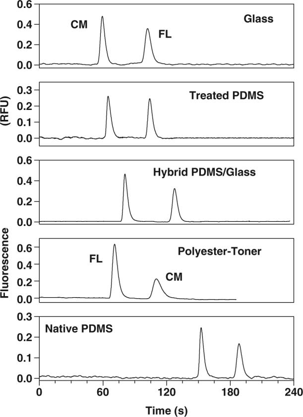
Example electropherograms for the separation of 25 μmol/L CM and FL using glass, plasma-treated PDMS, hybrid PDMS/glass, PT, and native PDMS chips. For gated injection, the electrical potentials applied to sample and buffer reservoirs were 1200 and 1800 V, respectively; the floating time was 1 s; channel effective length, 40 mm from injector. All electropherograms were recorded with normal polarity, except for PT chips (negative polarity).
The separation performance of these devices is compared in Table 2 in terms of plate numbers, N, and peak symmetry, expressed as peak skew. Efficiency was calculated according to the equation N = 5.54 × (tm/w1/2)2, where tm is the migration time and w1/2 is the peak width at half-height. Microcal™ Origin™ software version 5.0 was used to integrate and analyze the data. The peak skew was measured using the same software employed to collect the fluorescence signal [61]. As one can see from Table 2, the best separation efficiencies were observed for native PDMS, which required a longer separation time compared with that of other materials (see Fig. 3). As presented in Table 2, the lower the EOF of the substrate, the higher the plate numbers, except for PT devices. The same trend was not observed on PT chips due to the use of reverse polarity associated with the analyte–wall interaction as well as the high channel roughness. In terms of peak skew, a perfectly symmetrical peak should have a value of 1.0. Values greater than 1.0 indicate the presence of tailing peaks [61]. The efficiency can be affected by the channel geometry (or channel surface uniformity), EOF magnitude, injection process, or even by analyte–wall interaction [39, 62].
Table 2.
Comparison of the separation efficiency and peak skew found for all microfluidic channel materials
| Materials | Efficiency (N) |
Peak skew |
||
|---|---|---|---|---|
| CM | FL | CM | FL | |
| Native PDMS | 6980 | 6265 | 1.28 | 1.20 |
| Hybrid PDMS/glass | 1865 | 3330 | 1.32 | 1.18 |
| Plasma-treated PDMS | 1265 | 2720 | 1.35 | 1.29 |
| Glass | 812 | 1410 | 1.24 | 1.17 |
| PT | 895 | 925 | 1.21 | 1.26 |
Figure 3.
Electropherogram showing the resolution variance over seven repetitive injections on native PDMS devices. Experimental conditions are the same as in Fig. 1.
The channel geometry is one of the most important parameters influencing the microchip electrophoresis performance [54, 62]. As various microfabrication methods were used, different channel shapes were obtained. Microfluidic channels composed of PDMS fabricated using rapid prototyping and replica molding exhibit channels that are rectangular in shape. Etching of glass with HF or BOE generates a trapezoidal shape in glass channels due to isotropic etching [54]. Lastly, the PT channel shape is defined by the resolution of the LP and is not perfectly regular due to the limitations discussed in Section 3.1. However, its geometry is very close to a cylindrical shape [24, 26, 37].
The injection plug length also has a significant influence on the separation efficiency. The plug length in gated injection is substantially influenced by the injection time, electric field strength, channel dimensions (width and depth), sample concentration, electrophoretic mobility of the analyte, and electroosmotic mobility. The experiments reported here were performed under the same electric field strength using microchips fabricated with similar channel dimensions but having different EOF values. Therefore, the amount injected varied depending on the substrate material directly influencing the separation efficiency.
Besides the effects of the channel geometry, EOF magnitude, and method of injection, additional factors can also negatively affect the separation efficiency. The contributions to total variance in microchip electrophoresis are:
| (2) |
where is from the molecular diffusion, is from the injection system, is from the detector system (laser beam spot-size length), is from analyte interaction to channel wall, and is from Joule heating [63]. Since all of the experimental parameters except the material substrate were kept constant in this work, the contributions of , , and to are constant. In addition, all material substrates exhibited efficient heat dissipation up to 500 V/cm so that can be considered negligible compared with .
Thus, any change in should be exclusively related to the contribution of . Peak variances at sequentially longer separation distances were measured and plotted as a function of increasing separation-channel effective length. The total variances for a 25 μmol/L FL peak were calculated using the Microcal™ Origin™ software. Figure 2 shows the results obtained for the total variance versus the detection point on the channel for each system investigated in this work. A linear correlation was observed for all of them. For PT chips at 40 mm, for example, was 1.8 × 10⁻² cm2. For a small molecule such as FL, the diffusion coefficient, Di, is ca. 1.0 × 10⁻⁵ cm2/s. Considering a migration time of 72.6 s, then is calculated to be 1.4 × 10⁻³ cm2 ( = 2Di × t). For PT chips, the injection plug length, lInj, was estimated be approximately 300 μm (540 pL). Since the EOF is different for each material, the injection plug length (or injection volume) was determined separately using fluorescence images (data not shown). Using the value of 300 μm, the contribution of the injection to the total variance () on PT chips was 7.5 × 10⁻⁵ cm2 (). Assuming that and have nearly equal contributions to the total variance and that is negligible, the was estimated to be 1.6 × 10⁻² cm2. These values indicate that was the largest contributor (ca. 90%) to the band broadening on PT electrophoretic devices. On glass, was determined to be 9.6 × 10⁻⁴ cm2, a value that represents 25% of .
Figure 2.
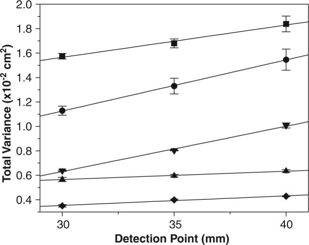
Peak total variance for 25 μmol/L FL as a function of detection point in (◆) glass, (▲) hybrid PDMS/glass, (▼) plasma-treated PDMS, (•) native PDMS, and (■) PT devices (n = 3). Experimental conditions are the same as in Fig. 1.
Overall, it can be seen in Fig. 2 that the channel walls of glass and hybrid PDMS/glass contribute less to than do other materials for the analytes employed in these experiments (anionic dyes). Glass and hybrid PDMS/glass devices exhibited similar slopes over three different detection points. A good correlation was also observed between native and plasma-treated PDMS devices. The significant variation on the for the native PDMS device is attributed to EOF instability. For the fluorescent dyes, the PT devices displayed lower separation efficiencies and exhibited greater wall adsorption compared with chips fabricated from glass and PDMS. The separation efficiency on PT devices could be improved by adding EOF modifier, thus reversing its direction, or by selecting positively charged analytes. In this case, electrophoresis could be performed under normal polarity on all substrate materials.
Similar results in terms of total variance have been obtained for glass channels fabricated using a toner-mediated lithographic technique [47]. In this case, the channel roughness was defined by the direct-printing process, such as the one used in the PT devices. However, the short manufacturing time and the very low cost of PT devices are significant advantages over other substrate materials. Obviously, a more realistic comparison of the analytical performance would be to evaluate all three substrates using a low-resolution technique for fabrication or making more defined PT channels with a higher resolution LP (>3000 dpi) [37]. In recent years, different procedures using toner have been described to fabricate PDMS [42-44], glass [47], and PT channels [24-26]. Using toner-based techniques to produce disposable devices, the roughness of the toner layer would be transferred to either the PDMS or glass surface during molding, thermal transference, or wet chemical etching. In this case, PT devices could present better analytical performance than low-resolution PDMS and glass channels.
3.5 Run-to-run reproducibility and ruggedness
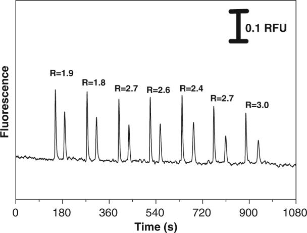
The run-to-run reproducibility was evaluated for all the materials. To evaluate the run-to-run reproducibility, an automatic sequence of seven injections was programmed for all microchips. The only variable was the time interval between injections due to the separation time differences for different substrates. The best results in terms of run-to-run repeatability were found on glass and hybrid PDMS/glass (data not shown). For an intra-chip comparison on glass and hybrid PDMS/glass chips, the RSD values in the migration time, peak area, peak height, and separation efficiency were lower than 8%. The plasma-oxidized PDMS devices also exhibited excellent run-to-run repeatability (data not shown). On these devices, an amazing stability over eight uninterrupted hours was obtained with low RSD in migration times (2.4−3.6%). For native PDMS, injections were performed every 120 s. An electropherogram showing seven sequential injections performed on native PDMS devices is shown in Fig. 3. The migration times for CM and FL were 159±5 and 200±10 s, respectively. The RSDs in peak height and peak area for CM and FL were 11.4 and 8.9 and 26.3 and 24.5%, respectively. The large RSDs for migration times, peak height, and peak area can be attributed to the instability of the EOF over the course of the seven injections, which varied as much as 10% (see Table 1). The RSD values for both peak height and peak area were greater for FL than for CM; this is due to the electrokinetic injection bias of the gated injection. The resolution of the two compounds also increased from 1.9 to 3.0 from the first injection to the seventh, as shown in Fig. 3. In addition, the peak skew value was systematically affected by the continuous change in EOF, giving RSDs of 2.6% (CM) and 5.9% (FL). This irreproducibility of EOF can be a problem for chips that will be used multiple times. However, one of the major advantages of both PDMS and PT chips is that they are very inexpensive and can thus be used for disposable single-use devices. In this case, long-term changes in the EOF are not important.
The run-to-run repeatability was also evaluated for PT devices. For PT chips, it was necessary to reverse the polarity in order to detect the negatively charged dyes. This is because the EOF generated by the PT chips is not large enough to allow the injection of a significant amount of the negative dyes using normal polarity. Figure 4 shows an electropherogram of seven repetitive injections performed every 120 s. The first injection resulted in peaks of low intensity when compared with the following six injections. This effect is attributed to low EOF, in which the electrokinetic transport on these devices requires a longer loading time to completely fill the microfluidic connections with sample. The migration times for FL and CM were, respectively, 66±3 and 104±8 s. The RSDs for both peak height and peak area over these seven injections were greater than 20%. If the data from the first injection are ignored, then the RSD values were better than 10%. A noticeable difference in resolution is observed after the first three injections on PT chips. The resolutions (for the two dyes) for first, second, and third injections were 2.7, 2.3, and 1.9, respectively. From the fourth to seventh injections, the resolutions ranged from 1.4 to 1.6. This decrease in resolution is also a result of EOF instability. The analytical performance in terms of repeatability on PT devices was slightly better than that of the native PDMS chips.
Figure 4.
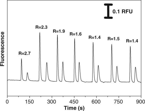
Electropherogram showing the fluorophores separation over seven repetitive injections on PT devices performed every 120 s.
4 Concluding remarks
The analytical performance comparison of electrophoresis microchips fabricated by standard procedures (photolithography and replica molding) and an emerging technique (direct-printing process) provides a useful reference to researchers developing microchip electrophoresis-based devices. Glass, native, and plasma-treated PDMS, hybrid PDMS/glass, and PT devices were fabricated according to the limiting dimensions (width/depth 150 μm/12 μm) from the direct-printing process. Based on our results, native PDMS and glass chips showed the lowest and the highest amount of heat dissipation, respectively. In addition, PT devices exhibited the lowest EOF among all substrate materials. The low EOF generated on PT channels was not high enough to detect negative dyes with normal polarity. The EOF magnitude was greater in glass and plasma-treated PDMS devices. Based on these results, PT devices could be useful for separations in which the EOF needs to be suppressed.
For the anionic dyes employed in our experiments, better efficiencies were obtained for PDMS/glass and native PDMS chips. Quantitative studies were carried out to demonstrate the contribution of the channel wall, , to the total variance, which for PT devices represents almost 90% of the total variance. On the other hand, for glass and hybrid PDMS/glass chips, the contribution of is lower than 30%.
Despite some drawbacks, PT chips have several advantages over the other chip substrates. The fabrication procedure is extremely simple and fast and employs equipment that is found in most offices (LP, transparencies, and a laminator). The chips are very inexpensive and can be considered disposable. They are also very lightweight and not fragile like glass. The results presented in this paper also show that the PT chips exhibit low EOF that could be useful for many biological applications. Although PT exhibits lower separation efficiencies than PDMS and glass, it is still possible to perform fast separations on these chips. PT chips may be most useful for point-of-care clinical applications where very cheap, rugged, and disposable devices are desirable. Future research will include the investigation of higher resolution LPs to produce narrower and better-defined microchannels and, therefore, improve the analytical performance of the devices, as well as the investigation of PT chips for the separation of peptides and proteins.
Acknowledgments
The authors thank Coordenadoria de Aperfeiçoamento de Pessoal de Ensino Superior (CAPES) (Grant No. BEX0706/02-1) for a fellowship for the development of this work and especially the Lunte group members for helpful discussions and technical support. National Institutes of Health (Grant No. NS049229), Fundação de Amparo à Pesquisa do Estado de São Paulo (FAPESP) (Grant No. 04/01525-0), and Conselho Nacional de Desenvolvimento Científico Tecnológico (CNPq) (Grant No. 478467/2006-0) are also recognized for providing financial support. Nancy Harmony is also acknowledged for editorial assistance.
Abbreviations
- BOE
buffered oxide etchant
- CM
coumarin
- DTL
double-toner layer
- FL
fluorescein
- LP
laser printer
- PET
polyethylene terephthalate
- PT
polyester-toner
- STL
single-toner layer
Footnotes
The authors have declared no conflict of interest.
5 References
- 1.Vilkner T, Janasek D, Manz A. Anal. Chem. 2004;76:3373–3385. doi: 10.1021/ac040063q. [DOI] [PubMed] [Google Scholar]
- 2.Dittrich PS, Tachikawa K, Manz A. Anal. Chem. 2006;78:3887–3907. doi: 10.1021/ac0605602. [DOI] [PubMed] [Google Scholar]
- 3.Auroux PA, Iossifidis D, Reyes DR, Manz A. Anal. Chem. 2002;74:2637–2652. doi: 10.1021/ac020239t. [DOI] [PubMed] [Google Scholar]
- 4.Reyes DR, Iossifidis D, Auroux PA, Manz A. Anal. Chem. 2002;74:2623–2636. doi: 10.1021/ac0202435. [DOI] [PubMed] [Google Scholar]
- 5.Dolnik V, Liu SR, Jovanovich S. Electrophoresis. 2000;21:41–54. doi: 10.1002/(SICI)1522-2683(20000101)21:1<41::AID-ELPS41>3.0.CO;2-7. [DOI] [PubMed] [Google Scholar]
- 6.Seiler K, Harrison DJ, Manz A. Anal. Chem. 1993;65:1481–1488. [Google Scholar]
- 7.Effenhauser CS, Manz A, Widmer HM. Anal. Chem. 1993;65:2637–2642. [Google Scholar]
- 8.Effenhauser CS, Manz A, Widmer HM. Anal. Chem. 1995;67:2284–2287. [Google Scholar]
- 9.McCreedy T. Trends Analyt. Chem. 2000;19:396–400. [Google Scholar]
- 10.Chen Y, Pepin A. Electrophoresis. 2001;22:187–207. doi: 10.1002/1522-2683(200101)22:2<187::AID-ELPS187>3.0.CO;2-0. [DOI] [PubMed] [Google Scholar]
- 11.Huynh BH, Fogarty BA, Martin RS, Lunte SM. Anal. Chem. 2004;76:6440–6447. doi: 10.1021/ac049365i. [DOI] [PubMed] [Google Scholar]
- 12.Becker H, Gartner C. Electrophoresis. 2000;21:12–36. doi: 10.1002/(SICI)1522-2683(20000101)21:1<12::AID-ELPS12>3.0.CO;2-7. [DOI] [PubMed] [Google Scholar]
- 13.Becker H, Locascio LE. Talanta. 2002;56:267–287. doi: 10.1016/s0039-9140(01)00594-x. [DOI] [PubMed] [Google Scholar]
- 14.Fiorini GS, Chiu DT. BioTechniques. 2005;38:429–446. doi: 10.2144/05383RV02. [DOI] [PubMed] [Google Scholar]
- 15.Shadpour H, Musyimi H, Chen J, Soper SA. J. Chromatogr. A. 2006;1111:238–251. doi: 10.1016/j.chroma.2005.08.083. [DOI] [PubMed] [Google Scholar]
- 16.Martynova L, Locascio LE, Gaitan M, Kramer GW, et al. Anal. Chem. 1997;69:4783–4789. doi: 10.1021/ac970558y. [DOI] [PubMed] [Google Scholar]
- 17.Galloway M, Stryjewski W, Henry A, Ford SM, et al. Anal. Chem. 2002;74:2407–2415. doi: 10.1021/ac011058e. [DOI] [PubMed] [Google Scholar]
- 18.Kelly RT, Woolley AT. Anal. Chem. 2003;75:1941–1945. doi: 10.1021/ac0262964. [DOI] [PubMed] [Google Scholar]
- 19.Liu Y, Ganser D, Schneider A, Liu R, et al. Anal. Chem. 2001;73:4196–4201. doi: 10.1021/ac010343v. [DOI] [PubMed] [Google Scholar]
- 20.Shadpour H, Hupert ML, Patterson D, Liu CG, et al. Anal. Chem. 2007;79:870–878. doi: 10.1021/ac0612168. [DOI] [PubMed] [Google Scholar]
- 21.Rossier JS, Schwarz A, Reymond F, Ferrigno R, et al. Electrophoresis. 1999;20:727–731. doi: 10.1002/(SICI)1522-2683(19990101)20:4/5<727::AID-ELPS727>3.0.CO;2-A. [DOI] [PubMed] [Google Scholar]
- 22.Fiorini GS, Jeffries GDM, Lim DSW, Kuyper CL, Chiu DT. Lab Chip. 2003;3:158–163. doi: 10.1039/b305074m. [DOI] [PubMed] [Google Scholar]
- 23.Fiorini GS, Lorenz RM, Kuo JS, Chiu DT. Anal. Chem. 2004;76:4697–4704. doi: 10.1021/ac0498922. [DOI] [PubMed] [Google Scholar]
- 24.do Lago CL, da Silva HDT, Neves CA, Brito-Neto JGA, da Silva JAF. Anal. Chem. 2003;75:3853–3858. doi: 10.1021/ac034437b. [DOI] [PubMed] [Google Scholar]
- 25.Coltro WKT, da Silva JAF, da Silva HDT, Richter EM, et al. Electrophoresis. 2004;25:3832–3838. [Google Scholar]
- 26.He FY, Liu AL, Yuan JH, Coltro WKT, et al. Anal. Bioanal. Chem. 2005;382:192–197. doi: 10.1007/s00216-005-3200-x. [DOI] [PubMed] [Google Scholar]
- 27.Piccin E, Coltro WKT, da Silva JAF, Neto SC, et al. J. Chromatogr. A. 2007;1173:151–158. doi: 10.1016/j.chroma.2007.09.081. [DOI] [PubMed] [Google Scholar]
- 28.Castaño-Álvarez M, Fernández-Abedul MT, Costa-García A. Electrophoresis. 2005;26:3160–3168. doi: 10.1002/elps.200500148. [DOI] [PubMed] [Google Scholar]
- 29.Duffy DC, McDonald JC, Schueller OJA, Whitesides GM. Anal. Chem. 1998;70:4974–4984. doi: 10.1021/ac980656z. [DOI] [PubMed] [Google Scholar]
- 30.McDonald JC, Duffy DC, Anderson JR, Chiu DT, et al. Electrophoresis. 2000;21:27–40. doi: 10.1002/(SICI)1522-2683(20000101)21:1<27::AID-ELPS27>3.0.CO;2-C. [DOI] [PubMed] [Google Scholar]
- 31.Anderson JR, Chiu DT, Jackman RJ, Chemiavskaya O, et al. Anal. Chem. 2000;72:3158–3164. doi: 10.1021/ac9912294. [DOI] [PubMed] [Google Scholar]
- 32.McDonald JC, Whitesides GM. Acc. Chem. Res. 2002;35:491–499. doi: 10.1021/ar010110q. [DOI] [PubMed] [Google Scholar]
- 33.Vickers JA, Caulum MM, Henry CS. Anal. Chem. 2006;78:7446–7452. doi: 10.1021/ac0609632. [DOI] [PubMed] [Google Scholar]
- 34.Fogarty BA, Heppert KE, Cory TJ, Hulbutta KR, et al. Analyst. 2005;130:924–930. doi: 10.1039/b418299e. [DOI] [PubMed] [Google Scholar]
- 35.Nielsen T, Nilsson D, Bundgaard F, Shi P, et al. J. Vac. Sci. Technol. B. 2004;22:1770–1775. [Google Scholar]
- 36.McCormick RM, Nelson RJ, Alonso-Amigo MG, Benvegnu DJ, Hooper HH. Anal. Chem. 1997;69:2626–2630. doi: 10.1021/ac9701997. [DOI] [PubMed] [Google Scholar]
- 37.Coltro WKT, Carrilho E. In: Handbook of Capillary and Microchip Electrophoresis and Associated Microtechniques. 3rd ed. Landers JP, editor. CRC Press; New York: 2007. pp. 1169–1184. [Google Scholar]
- 38.Li MW, Huynh BH, Hulvey MK, Lunte SM, Martin RS. Anal. Chem. 2006;78:1042–1051. doi: 10.1021/ac051592c. [DOI] [PubMed] [Google Scholar]
- 39.Lacher NA, Rooji NF, Verpoorte E, Lunte SM. J. Chromatogr. A. 2003;1004:225–235. doi: 10.1016/s0021-9673(03)00722-2. [DOI] [PubMed] [Google Scholar]
- 40.Liu AL, He FY, Hu YL, Xia XH. Talanta. 2006;68:1303–1309. doi: 10.1016/j.talanta.2005.07.043. [DOI] [PubMed] [Google Scholar]
- 41.Liu AL, He FY, Wang K, Zhou T, et al. Lab Chip. 2005;5:974–977. doi: 10.1039/b502764k. [DOI] [PubMed] [Google Scholar]
- 42.Bao N, Zhang Q, Xu JJ, Chen HY. J. Chromatogr. A. 2005;1089:270–275. doi: 10.1016/j.chroma.2005.07.001. [DOI] [PubMed] [Google Scholar]
- 43.Vullev VI, Wan JD, Heinrich V, Landsman P, et al. J. Am. Chem. Soc. 2006;128:16062–16072. doi: 10.1021/ja061776o. [DOI] [PubMed] [Google Scholar]
- 44.Kaigala GV, Ho S, Penterman R, Backhouse CJ. Lab Chip. 2007;7:384–387. doi: 10.1039/b617764f. [DOI] [PubMed] [Google Scholar]
- 45.do Lago CL, de Jesus DP, da Silva HDT, Neves CA, da Silva JAF. Electrophoresis. 2004;25:3825–3832. [Google Scholar]
- 46.de Jesus DP, Blanes L, do Lago CL. Electrophoresis. 2006;27:4935–4941. doi: 10.1002/elps.200600137. [DOI] [PubMed] [Google Scholar]
- 47.Coltro WKT, Piccin E, da Silva JAF, do Lago CL, Carrilho E. Lab Chip. 2007;7:931–934. doi: 10.1039/b702931d. [DOI] [PubMed] [Google Scholar]
- 48.Richter EM, da Silva JAF, do Lago CL, Angnes L. Electrophoresis. 2004;25:2965–2970. doi: 10.1002/elps.200305960. [DOI] [PubMed] [Google Scholar]
- 49.Daniel D, Gutz IGR. Electrochem. Commun. 2003;5:782–790. [Google Scholar]
- 50.Daniel D, Gutz IGR. Talanta. 2005;68:429–435. doi: 10.1016/j.talanta.2005.09.003. [DOI] [PubMed] [Google Scholar]
- 51.Huynh BH, Fogarty BA, Nandi P, Lunte SM. J. Pharm. Biomed. Anal. 2006;42:529–534. doi: 10.1016/j.jpba.2006.05.014. [DOI] [PubMed] [Google Scholar]
- 52.Lacher NA, Martin RS, Lunte SM. Anal. Chem. 2004;76:2482–2491. doi: 10.1021/ac030327t. [DOI] [PubMed] [Google Scholar]
- 53.Kikuna-Hanajini R, Scott Martin R, Lunte SM. Anal. Chem. 2002;74:6370–6377. doi: 10.1021/ac0204000. [DOI] [PubMed] [Google Scholar]
- 54.Kim M-S, Cho S, Lee K-N, Kim Y-K. Sens. Actuators B. 2005;107:818–824. [Google Scholar]
- 55.Huang XH, Gordon MJ, Zare RN. Anal. Chem. 1988;60:1837–1838. [Google Scholar]
- 56.Mourzina Y, Steffen A, Kalyagin D, Carius R, Offenhausser A. Electrophoresis. 2005;26:1849–1860. doi: 10.1002/elps.200410295. [DOI] [PubMed] [Google Scholar]
- 57.Fletcher PDI, Haswell SJ, Zhang X. Lab Chip. 2001;1:115–121. doi: 10.1039/b106339c. [DOI] [PubMed] [Google Scholar]
- 58.Mourzina Y, Kalyagin D, Steffen A, Offenhausser A. Talanta. 2006;70:489–498. doi: 10.1016/j.talanta.2005.12.063. [DOI] [PubMed] [Google Scholar]
- 59.Ren Z, Bachman M, Sims C, Li GP, Allbritton N. J. Chromatogr. B. 2001;762:117–125. doi: 10.1016/s0378-4347(01)00327-9. [DOI] [PubMed] [Google Scholar]
- 60.Qiao R. Microfluid. Nanofluid. 2007;3:33–38. [Google Scholar]
- 61.Martin RS, Ratzlaff KL, Huynh BH, Lunte SM. Anal. Chem. 2002;73:1136–1143. doi: 10.1021/ac011087p. [DOI] [PubMed] [Google Scholar]
- 62.Pu Q-S, Luttge R, Gardeniers HJGE, van der Berg A. Electrophoresis. 2003;24:162–171. doi: 10.1002/elps.200390009. [DOI] [PubMed] [Google Scholar]
- 63.Baker DR. Capillary Electrophoresis. Wiley; New York: 1995. [Google Scholar]