Abstract
The authors are investigating the concept of a direct-conversion flat-panel imager with avalanche gain for low-dose x-ray imaging. It consists of an amorphous selenium (a-Se) photoconductor partitioned into a thick drift region for x-ray-to-charge conversion and a relatively thin region called high-gain avalanche rushing photoconductor (HARP) in which the charge undergoes avalanche multiplication. An active matrix of thin film transistors is used to read out the electronic image. The authors call the proposed imager HARP active matrix flat panel imager (HARP-AMFPI). The key advantages of HARP-AMFPI are its high spatial resolution, owing to the direct-conversion a-Se layer, and its programmable avalanche gain, which can be enabled during low dose fluoroscopy to overcome electronic noise and disabled during high dose radiography to prevent saturation of the detector elements. This article investigates key design considerations for HARP-AMFPI. The effects of electronic noise on the imaging performance of HARP-AMFPI were modeled theoretically and system parameters were optimized for radiography and fluoroscopy. The following imager properties were determined as a function of avalanche gain: (1) the spatial frequency dependent detective quantum efficiency; (2) fill factor; (3) dynamic range and linearity; and (4) gain nonuniformities resulting from electric field strength nonuniformities. The authors results showed that avalanche gains of 5 and 20 enable x-ray quantum noise limited performance throughout the entire exposure range in radiography and fluoroscopy, respectively. It was shown that HARP-AMFPI can provide the required gain while maintaining a 100% effective fill factor and a piecewise dynamic range over five orders of magnitude (10−7–10−2 R∕frame). The authors have also shown that imaging performance is not significantly affected by the following: electric field strength nonuniformities, avalanche noise for x-ray energies above 1 keV and direct interaction of x rays in the gain region. Thus, HARP-AMFPI is a promising flat-panel imager structure that enables high-resolution fully quantum noise limited x-ray imaging over a wide exposure range.
Keywords: flat-panel detector, avalanche gain, amorphous selenium, fluoroscopy
INTRODUCTION
There has been much work over the last decade on development of active matrix flat-panel imagers (AMFPI) based on thin film transistor (TFT) arrays. These self-scanned digital solid-state x-ray imaging systems are replacing conventional film screen and computed radiography systems in a number of radiographic applications. Modern AMFPI systems provide excellent image quality and enable the image to be read out rapidly in digital form and subsequently be displayed and archived. Furthermore, AMFPI systems are compact and produce negligible geometrical image distortion. For these reasons, they have significant potential to replace the x-ray image intensifier in radiographic∕fluoroscopic (R∕F) applications as well as in advanced tomographic applications such as digital tomosynthesis and cone-beam computed tomography.
In the present article, we will review the limitations of current AMFPI systems, pertaining in particular to their performance in very low exposure applications (i.e., fluoroscopy and tomography). These limitations result from the presence of noise in the readout electronics of the imager.1, 2, 3 We will next present an AMFPI structure capable of overcoming the electronic noise and model its imaging performance throughout a wide range of x-ray exposures. The imager structure discussed in this article should enable high-resolution R∕F x-ray imaging with sensitivities that are equivalent to modern XRII imagers in a compact solid-state system, extending the quantum noise limited imaging performance of AMFPIs to advanced clinical applications requiring low dose.
TECHNICAL BACKGROUND
Requirements for an ideal R∕F imager
An essential requirement for a R∕F imager is to support both radiographic and fluoroscopic modes of operation. An ideal dual-mode imager should provide excellent imaging resolution—particularly in the radiographic mode—and quantum-noise limited x-ray sensitivity—particularly in the fluoroscopic mode. The imager should also be compact, capable of operating at high frame rates (up to 30 frames per second) and have a linear response over five orders of magnitude (from 10−7 to 10−2 R per frame).4
Indirect and direct conversion imagers
AMFPI systems are categorized as either direct conversion or indirect conversion. In an indirect conversion imager, x-ray photons strike a scintillator such as cesium iodide (CsI) and generate optical photons which then interact with a photodiode (usually made from amorphous silicon), in turn producing electron-hole pairs (EHPs) that are stored prior to being processed by the active matrix readout electronics. In contrast, for direct conversion imagers, x rays interact with a photoconductor, usually amorphous selenium (a-Se), and directly generate EHPs which can be collected and read out by the active matrix. Direct conversion imagers have the important advantage of higher image resolution because the charged image carriers travel along the electric field lines in the photoconductor and are not prone to diffusion, unlike neutral photons in a scintillator. Furthermore, owing to the absence of a photodiode, the simpler TFT array readout structure used in direct conversion imagers can be manufactured in a standard commercial facility for active matrix liquid crystal displays.5 For these reasons, we have chosen to focus only on direct conversion x-ray imagers in the present article. However, neither type of imager is currently quantum noise limited at the low exposures of the fluoroscopic region, 10−7–10−6 R∕frame.3, 6, 7
Electronic noise in AMFPI
An exposure of 10−7 R∕frame in an a-Se AMFPI with 250×250 μm detector elements (del) is equivalent on average to a single x-ray photon striking each del for each frame. A 50 keV photon generates a signal of ∼1000 electrons in an a-Se photoconductor biased at 10 V∕μm.8 Thus, to reliably detect this signal (assuming a signal-to-noise ratio of 5), the electronic noise level should not exceed ∼200 e at each del. However, the electronic noise in the readout system of a large modern AMFPI (Ref. 2) is on the order of 1500 e per del, which prevents single x-ray detection.
The electronic noise problem in AMFPIs at low exposures may, in principle, be overcome by providing a gain stage at each del that amplifies the x-ray generated charge. Recently, there have been three possible solutions proposed for providing gain at each del. First, high conversion gain photoconductors are being developed which generate larger numbers of EHPs for each incident x-ray photon, thus providing a stronger signal than a-Se.9, 10 Second, readout circuits known as active pixels that incorporate a low-noise analog amplifier at each del have been devised and have been shown to reduce the significance of electronic noise.11, 12, 13 The third approach, and the one adopted in this work, makes use of avalanche multiplication in the bulk of a-Se.
The first two approaches provide adequate gain to overcome electronic noise at low exposures, however, this gives rise to another problem: the gain is too high at larger exposures and this leads to an increase in potential across the del capacitance which can cause breakdown of the thin oxide of the del capacitance. Furthermore, both approaches also have other inherent limitations. High gain photoconductors such as PbI2 or HgI2 are difficult to deposit into large defect-free areas, suffer from limited charge range and raise environmental concerns. Active pixels, on the other hand, are difficult to implement in conventional TFT manufacturing processes, may require larger del sizes, and are prone to radiation damage. In light of these limitations, we are investigating the third approach which involves avalanche multiplication in a-Se to better understand the advantages and potential disadvantages of this approach.
Imaging systems with avalanche multiplication
Avalanche multiplication is a physical process in which impact ionization of charge produces charge amplification. It has been used in radiographic gas imagers as early as 1965, when Reiss developed an image-forming chamber which relied on avalanche multiplication of electrons in a gas.14 The associated gain helped overcome the low sensitivity of previous imagers and it provided better sensitivity than a-Se imaging plates. However, it was later recognized by Boag15 that the avalanche process produces a “random assortment of large charge deposits,” which significantly degrade the image quality.15 This was attributed to secondary electrons initiating avalanche multiplication at various depths in the gas, thus contributing to a depth-dependent gain fluctuation noise.
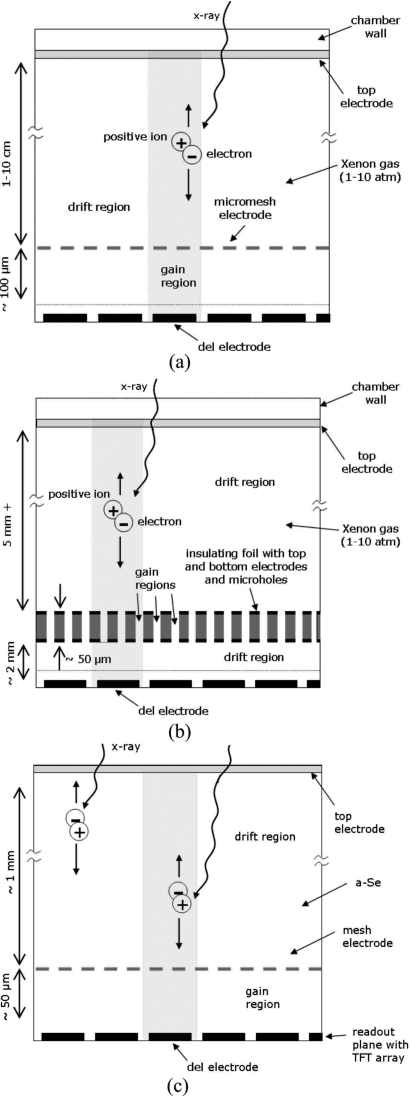
The depth-dependent gain problem may be overcome, in principle, by dividing the imaging chamber into a conversion or drift region in which impinging radiation ionizes the gas and generates free electrons and an amplification or gain region in which the electrons avalanche. Two CERN developments, the micromesh gaseous structure16 (MICROMEGAS) and the gas electron multiplier17, 18 (GEM) use this approach. A conceptual diagram of both devices is shown in Fig. 1. The depth-dependent gain problem has been overcome so successfully in these devices that they can provide excellent energy resolutions. This, combined with their good temporal resolution has enabled their use in photon counting applications.19 However, high gas pressures (several atmospheres) and thick layers of gas (several centimeters) are required to provide reasonable quantum efficiencies at radiographic energies. The window of the imaging chamber needs to be made sufficiently thick to support the high gas pressures, which limits the quantum efficiency. The large gas thickness also leads to a degradation of imaging resolution for obliquely-incident x rays. This may be corrected for by using a spherical detector geometry,15 however, this is often impractical.
Figure 1.
Cross sectional diagrams showing the concept of (a) MICROMEGAS and (b) GEM, where x rays ionize a gas and the resulting electrons undergo avalanche in a gain region. (c) Cross sectional diagram showing a solid state a-Se structure proposed by Lee (Ref. 32) in which the a-Se layer is partitioned into drift and gain regions. Shaded areas denote region of a single del.
Avalanche multiplication is known to occur in solid state semiconductors such as crystalline silicon. However, due to its poor linear x-ray absorption coefficient associated with its low atomic number (Z=14), crystalline silicon is of limited use as a direct-conversion x-ray image receptor. Furthermore, because it is a crystalline material, it is difficult to manufacture in large areas. This suggests the use of amorphous materials such as a-Se.
Amorphous selenium and avalanche multiplication
a-Se is a very well characterized material used in a number of AMFPI systems and has a long history of use in radiographic imaging plates.20, 21, 22 It has been the photoconductor of choice for direct-conversion imagers, due to its high intrinsic resolution, low dark current, good charge transport, and reasonably high x-ray absorption (Z=34) at most radiographic energies.23 The manufacturing process, which uses large-area thermal evaporation, is well established and relatively inexpensive, largely because it is a relatively low temperature process (T=450 °C).
Avalanche multiplication in a-Se was discovered by Juska in 1980. (Ref. 24) and later enabled the development and commercialization by Tanioka et al. at NHK Science and Technical Research Laboratories of a broadcasting camera which is more sensitive than the human eye.25, 26 The high-gain avalanche rushing photoconductor (HARP) camera demonstrated stable and spatially uniform optical imaging with avalanche multiplication gains as high as a thousand.25 Recently, work in our laboratory has indicated that the use of avalanche multiplication in a-Se is an effective means of providing gain for low exposure medical imaging applications.8, 27 We have previously proposed an indirect-conversion imager which makes use of a CsI phosphor optically coupled to an avalanche a-Se layer.28 In the present article, we introduce a direct-conversion imager which should meet the high sensitivity requirements of fluoroscopy and, in addition, provides excellent radiographic spatial resolution. Because avalanche gain is a function of the electric field applied across the a-Se layer, the gain may easily be adjusted to best suit a given imaging mode: a high avalanche gain may be used in fluoroscopy to overcome electronic noise and the gain may be removed at larger radiographic exposures. This results in a very wide piecewise dynamic range.
Existing a-Se avalanche layers, developed by Tanioka and co-workers, establish a uniform electric field throughout the bulk of the a-Se layer.25, 26 This is suitable for detection and imaging of photons in the visible spectrum, which are mostly absorbed at the surface of the photoconductor. Detection and imaging of x rays is complicated by the fact that the higher energy photons on average penetrate deeper into the photoconductor prior to absorption and generation of EHPs. At diagnostic x-ray energies, an a-Se layer thickness of 200–1000 μm is required in order to achieve a reasonable quantum efficiency.5 Establishing avalanche multiplication throughout such thick layers of a-Se is problematic because very high potentials (20–100 kV) need to be applied to reach avalanche fields (∼100 V∕μm), and absorption of x rays at different depths in the avalanche layer produces gain fluctuation noise.27, 29, 30 To suppress this depth-dependent gain fluctuation noise, the a-Se layer needs to be partitioned into a low-field drift region and a high-field gain region, analogously to the MICROMEGAS gaseous detector16 shown in Fig. 1a. The concept of such a dual-layered a-Se structure has been presented earlier.4, 31
PROPOSED DEVICE STRUCTURE
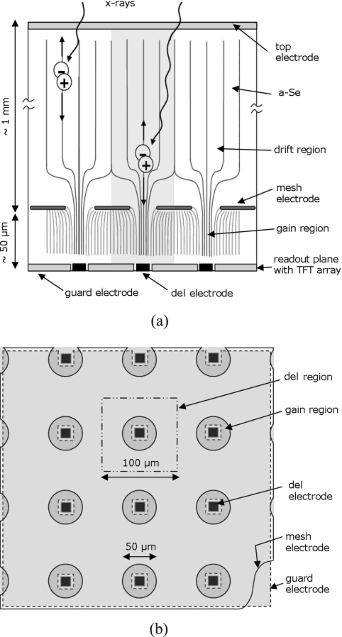
In light of what has been discussed in the previous section, we propose the HARP-AMFPI structure shown in Fig. 2. Figure 2a shows a cross section of the device. It consists of a thick (∼1000 μm) a-Se drift region, in which x rays are absorbed and generate EHPs. The electric field in this region is comparable to what is currently used in direct-conversion a-Se imagers (10 V∕μm).7, 23 A mesh electrode sets up a higher electric field (70–110 V∕μm) in the thin (∼10–50 μm) gain region. As shown, the electric field lines are shaped in such a way that most holes that drift towards the mesh electrode enter the gain region and undergo avalanche multiplication. The top view of the device is shown in Fig. 2b.
Figure 2.
(a) Side view showing the structure of HARP-AMFPI. The a-Se photoconductor is used to detect x rays and convert them to charge in the drift region. Holes undergo avalanche multiplication in the gain region and are collected at the del electrodes. Shaded area denotes region of a single del. Electric field lines are shown as continuous lines. (b) Top view of the HARP-AMFPI structure. The square area (dotted line) at the top denotes the region of a single del.
The top and mesh electrodes have blocking contacts to prevent holes from being injected. The x-ray generated holes entering the gain region are tightly focused and are absorbed by the del electrodes, in which the charge is stored on del capacitors and is periodically read out by a TFT array. Guard electrodes are used to establish a uniform potential in the readout plane of the AMFPI. Blocking contacts on the guard and del electrodes prevent electrons from being injected into the high-field region.
Lee et al. have recently proposed a solid-state imager using a-Se,31 shown in Fig. 1c, consisting of distinct drift and gain regions. Our structure in Fig. 2, however, differs in two important ways. First, the mesh electrode apertures are larger (on the same order as the del size) and are aligned with the del electrodes. Second, guard electrodes are used in the readout plane of the imager. Both these differences in structure enable a significant reduction in dark current and the amount of noise resulting from direct x-ray interaction in the gain region, as will be discussed in Sec. 6.
CALCULATION METHODS
In what follows is a description of the calculation methods used for a theoretical investigation of this proposed AMFPI structure. This includes an analysis of the imagers’s detective quantum efficiency (DQE) over a range of spatial frequencies f as well as a determination of the gain nonuniformities arising from electric field strength nonuniformities. The linearity of the del response to x-ray exposure will also be investigated.
MTF, NPS, and DQE
The MTF associated with EHP generation in a-Se is dependent on physical effects such as Compton scattering of x-ray photons in the material, diffusion and space charge effects. The model developed by Que et al.32 was used to obtain the a-Se MTF used in this work.
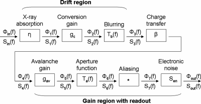
The DQE model was obtained from cascaded linear systems theory.33 Our implementation ignores second-order effects such as K-fluorescence reabsorption. Shown in Fig. 3 is a flow diagram of the signal and noise propagation through the various stages of the complete imaging system in Fig. 2. The noise at the output of the system prior to aliasing and the addition of electronic noise is given by
| (1) |
where Tb(f) and Ta(f) are the MTFs associated with EHP generation in a-Se and the del aperture function, respectively. The number of incident x-ray photons per unit area and the charge coupling efficiency between the drift and gain regions are denoted by q0 and β. ASe, η, and gc are the Swank factor, x-ray quantum absorption efficiency, and x ray to charge conversion gain of amorphous selenium, respectively. The avalanche gain and its variance are denoted by gav and , respectively.
Figure 3.
Flow diagram showing the stages of the cascaded linear system model for HARP-AMFPI.
Both charge conversion and avalanche multiplication of charge are nondeterministic processes, and hence, have a certain amount of noise associated with them. Each x-ray generates a variable number of EHPs in the a-Se layer, and this variation in conversion gain is characterized by ASe. Each hole that dissociates from an electron, in turn, undergoes a variable amount of avalanche multiplication. The variance of this process is represented by . In the case where only holes avalanche, which is a valid assumption for a-Se biased near 100 V∕μm,8, 27 Tager34 derived the relationship for the avalanche variance
| (2) |
used in our model. The holes generated by a single x-ray photon interaction each undergo avalanche multiplication, and the avalanche Swank factor Aav, which can be expressed as
| (3) |
denotes the overall variation in avalanche gain associated with this single x-ray interaction. This, however, is under the assumption that each hole that undergoes avalanche multiplication travels along the same path through the a-Se. In practice, holes travel along different paths in the gain region of the AMFPI and are subject to varying electric field strengths along these paths. This effect is characterized by the secondary Swank factor Asec which accounts for avalanche gain variations due to differences in travel paths for holes generated by a single x-ray interaction. Table 1 summarizes these various factors used to quantify the conversion and avalanche gain variation. Using Eqs. 1, 3 and including the effect of path length variation, the noise may simply be expressed as
| (4) |
The aliased noise variance S7(f) is given by aliasing the noise power spectrum (NPS) given by Eq. 4 with respect to the Nyquist frequency 1∕2ap, where ap is the del size. The output NPS, Sout(f) is given by the addition of the electronic noise variance Sn to the aliased noise variance. The normalized output NPS is then given by
| (5) |
and the DQE is taken as
| (6) |
Table 1.
Summary of factors used to characterize nonuniformities in conversion and avalanche gain. N∕A denotes that no information is available.
| Factor | Description | Published values | Values used in this work | |
|---|---|---|---|---|
| ASe | a-Se Swank factor | Each x-ray generates a variable number of electron-hole pairs in a- Se (conversion gain) | 0.961 | 0.96 |
| Avalanche variance | Each hole undergoes a variable amount of avalanche multiplication | 2 for gav=22 90 for gav=102 | 2 for gav=2 90 for gav=10 | |
| Aav | Avalanche Swank factor | All holes generated by one x-ray produce a variable amount of charge via avalanche multiplication | N∕A | 0.9993 |
| Secondary avalanche variance | Each hole undergoes a variable amount of avalanche multiplication due to different travel paths | N∕A | 3 for gav=104 | |
| Asec | Secondary avalanche Swank factor | All holes generated by one x-ray produce a variable amount of charge due to different travel paths during avalanche multiplication | 0.55 | 14 |
Table 2 summarizes the values of all AMFPI design parameters and operating conditions chosen for R∕F applications.
Table 2.
Detector operating conditions and design parameters chosen for fluoroscopy and radiography.
Avalanche gain, gain nonuniformities, and fill factor
Numerical calculations based on the finite element method (FEM) were done in MATLAB (Mathworks, Natick, MA) and used to obtain the distribution of the electric field in the proposed AMFPI structure. The imager parameters of interest were the mesh electrode aperture size, the separation between the mesh electrode and the image readout plane and the electric field in the drift and gain regions. Key AMFPI metrics were calculated and plotted. These include the average avalanche gain, the nonuniformities in avalanche gain arising from electric field strength nonuniformities, and the fill factor, which is the fraction of x-ray generated holes that is collected by the del electrodes. Our model enabled the investigation of a large parameter space and the optimization of the DQE for high performance R∕F applications.
The currently accepted model for charge transport in a-Se states that charge in selenium acquires energy when subjected to an external electric field and, in doing so, undergoes both elastic and inelastic collisions.35 The bend radius of the electric field lines in our proposed AMFPI structure is on the order of micrometers, which is much larger than the mean free paths of elastic and inelastic collisions, 0.6 and 7.2 nm, respectively.35, 36 Hence, the field lines obtained from our FEM analysis will coincide with the charge carrier travel paths. The avalanche gain gav is obtained by integrating the incremental gains experienced by a single charge traveling along a given field line according to
| (7) |
where d is the total path length along the field line, E(s) is the electric field strength at a point s along the path, and β1 and β2 are the impact ionization coefficients for a-Se.8, 37 The nonuniformity of the avalanche gain due to field strength nonuniformities was assessed by comparing the avalanche gain experienced by charge traveling along the central and lateral field lines arriving at the same del electrode.
Del response
For R∕F, the imager signal should have a piecewise linear response as a function of exposure over a range of up to five orders of magnitude. At the largest exposures, or with high avalanche gain, the amount of charge generated at each del can lead to an increase in potential of the del electrode to the point of dielectric breakdown of the TFT gate oxide.
This problem can be adressed by protecting the TFTs from high voltage damage using a dual-gate TFT structure.38 This will, however, lead to del saturation, meaning that no useful signal may be obtained. Also, close to saturation, linearity can be affected because the increase in potential of the del electrode during the exposure can decrease the electric field strength in the del gain region. This, in turn, can potentially reduce the avalanche gain, which is very sensitive to the field strength and result in a nonlinear del response.
To determine potential nonlinearities in the del response, each del may be modeled as two series capacitors, namely the intrinsic a-Se capacitance occurring between the top and del electrodes [see Fig. 2a], and the del storage capacitance used to integrate the signal charge. The a-Se capacitance in our proposed AMFPI structure is very small (∼0.5 fF) due to the large thickness of the a-Se layer (1000 μm). Hence, the much larger del storage capacitance (⩾200 fF) largely determines the del response. In modeling the latter, we assume the worst case scenario in which an x-ray pulse produces holes which avalanche and produce more holes. These holes accumulate on the del storage capacitance, decrease the avalanche field, which decreases the gain, thus reducing the amount of charge generated for an identical successive x-ray pulse.
RESULTS
MTF, NPS, and DQE
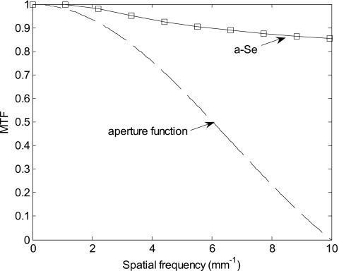
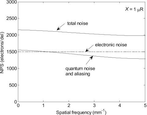
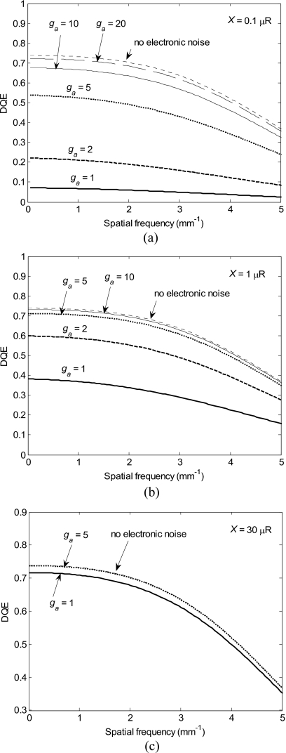
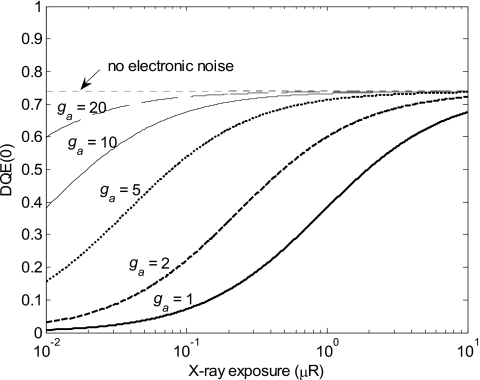
Shown in Fig. 4 is the MTF associated with direct x-ray interaction in a-Se obtained from our numerical model.32 The noise power spectrum was obtained using Eq. 4 and is presented in Fig. 5, for an average fluoroscopic exposure of 10−6 R∕frame. The DQE, calculated using Eq. 6, is shown for different avalanche gain factors in Fig. 6 for several exposures ranging from the lowest exposure occurring in fluoroscopy (10−7 R∕frame) to a radiographic exposure of 3×10⁻⁵ R∕frame. Figure 7, also obtained using Eq. 6, demonstrates the relationship between DQE(0) and the per-frame exposure at different avalanche gains throughout the fluoroscopic exposure range.
Figure 4.
Calculated MTF for a-Se and aperture function for detector with 100 μm del size.
Figure 5.
Comparison of the NPS before and after the addition of electronic noise at an average fluoroscopic exposure of 10−6 R∕frame and for operating conditions shown in Table 2.
Figure 6.
DQE(f) calculated using the detector parameters and operating conditions shown in Table 2 for an x-ray exposure of (a) 1×10⁻⁷, (b) 1×10⁻⁶, and (c) 3×10⁻⁵ R∕frame and varying levels of gain. For large enough gains, DQE(f) approaches the theoretical limit where there is no electronic noise (top-most curve in each graph). This represents the quantum noise limited DQE(f).
Figure 7.
DQE(0) calculated as a function of x-ray exposure using the detector parameters and operating conditions shown in Table 2 and varying levels of gain. For large gains, DQE(0) approaches the theoretical limit where there is no electronic noise (top-most curve). This represents the quantum noise limited DQE(0).
Avalanche gain, gain nonuniformities, and fill factor
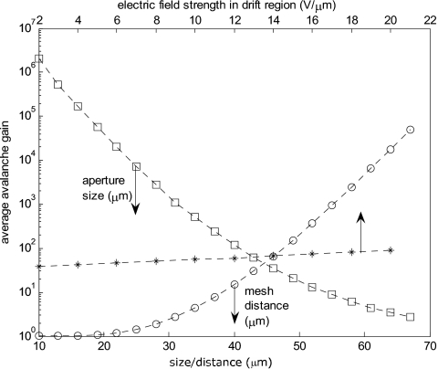
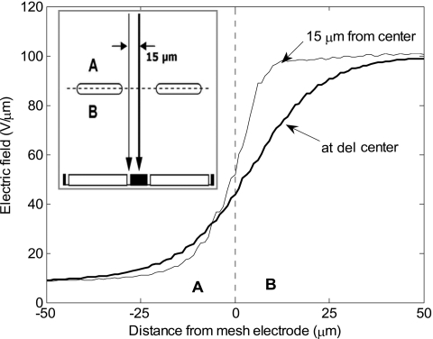
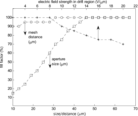
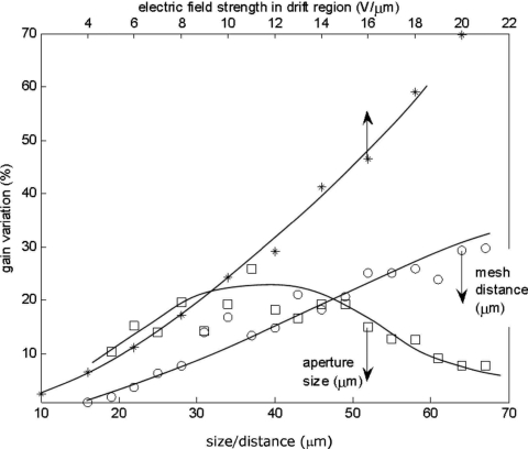
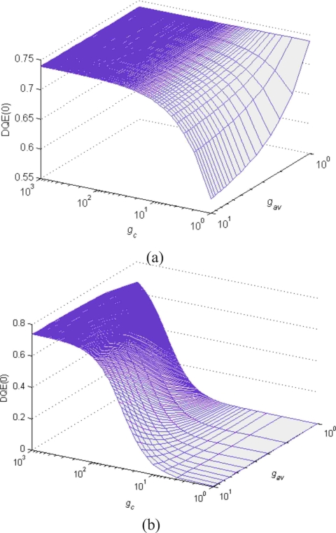
The average avalanche gain of the device, obtained using Eq. 7, varies as a function of aperture size and mesh distance and is shown in Fig. 8. The effect of changing the electric field strength in the drift region is also shown. Figure 9 depicts the distribution of the electric field strength in the direction normal to the readout plane and calculated at different distances from the mesh electrode. Shown are the field distributions at the del center and 15 μm away from the center. Calculated fill factors are presented in Fig. 10 and Fig. 11 shows how the gain nonuniformity, associated with this nonuniform field-strength distribution, changes as a function of aperture size, mesh distance, and the electric field strength in the drift region. The relative significance of the conversion and avalanche gains gc and gav is shown in Fig. 12 for the case where the imager is quantum noise limited and at an exposure of 10−6 R∕frame.
Figure 8.
Average avalanche gain calculated as a function of aperture size, mesh distance, and the electric field strength in the drift region. The detector parameters and operating conditions used are shown in Table 2.
Figure 9.
Comparison between the electric field strength experienced by a charge that travels from the drift region (region A) into the gain region (region B) along an axis that crosses the del center (denoted by the thick solid line) and along an axis 15 μm from the del center (denoted by the thin solid line), as shown in the inset at the top left. The direction of increasing distance is towards the del electrode.
Figure 10.
Effective fill factor calculated as a function of aperture size, mesh distance, and the electric field strength in the drift region. The detector parameters and operating conditions used are shown in Table 2.
Figure 11.
Gain nonuniformity calculated as a function of aperture size, mesh distance, and the electric field strength in the drift region. The detector parameters and operating conditions used are shown in Table 2.
Figure 12.
DQE(0) calculated as a function of conversion gain gc and avalanche gain gav using the detector parameters and operating conditions shown in Table 2 for (a) an infinitely large x-ray exposure (quantum noise limited case) and (b) an average fluoroscopic x-ray exposure of 10−6 R∕frame.
Del response
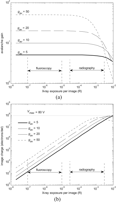
The effect associated with the decrease in gain due to the accumulation of charge on the del storage capacitance is shown in Fig. 13a. This effect was investigated for a range of x-ray exposures and several different avalanche gains. The reduction in avalanche gain was calculated using the numerical model described in Sec. 4B. and based on Eq. 7. The amount of charge stored at each del as a function of x-ray exposure is shown in Fig. 13b, for a 200 fF del storage capacitance.
Figure 13.
(a) Avalanche gain calculated as a function of x-ray exposure for varying levels of nominal avalanche gain gav. A del storage capacitor Cp of 200 fF was assumed. (b) Calculated image charge on each del electrode as a function of x-ray exposure for varying levels of nominal avalanche gain gav (Cp=200 fF) was assumed.
DISCUSSION
We shall discuss the theoretical effects of electronic noise in HARP-AMFPI with 100 μm del size, and how the presence of the avalanche gain stage changes DQE(f) at fluoroscopic and radiographic exposures. Next, we will examine the significance of various noise sources introduced in HARP-AMFPI. We will also examine the fill factor, del response, dark current, as well as the effect of direct x-ray interaction in the gain layer of the imager.
MTF, NPS, and DQE
Amorphous selenium has been used in direct-conversion AMFPIs because it is a well-characterized material and has a high intrinsic imaging resolution.4, 5, 20, 32 As seen in the calculated MTF curve (Fig. 4), despite Compton scattering, charge diffusion, and space charge effects, the degradation of the a-Se MTF is less than 15% at a spatial frequency of 10 mm−1. In comparison, the aperture function drops more rapidly, thus, for the AMFPI structure investigated in the present article, the spatial resolution is limited not by the photoconductor, but rather by the del size (100 μm) and the associated del aperture function.
Applying the cascaded linear system model in Fig. 3 we obtain the NPS in Fig. 5 for a conventional direct-conversion a-Se AMFPI with 100 μm del size at an average fluoroscopic exposure of 10−6 R∕frame. The presence of an output electronic noise of 1500 electrons per del root-mean-square (rms) increases the NPS at all spatial frequencies by over 40%. Electronic noise is thus a significant component of the NPS at 10−6 R∕frame.
Using the calculated MTF(f) and NPS(f), we obtain the spatial frequency dependent DQE in Fig. 6 for a range of x-ray exposures. As expected, we see that the presence of an avalanche gain stage provides a significant improvement in DQE: an avalanche gain of 20 at a fluoroscopic exposure of 10−7 R∕frame increases the DQE by nearly an order of magnitude in the 0–5 mm−1 spatial frequency range (Fig. 6). Furthermore, optimal DQE(0) is sustained throughout the entire fluoroscopic exposure range and a reduction of only 18% occurs at an exposure of 10−8 R∕frame, as observed in Fig. 7. Thus, for HARP-AMFPI with 100 μm del size, an avalanche gain of 20 is sufficient for quantum noise limited operation at all clinically relevant R∕F exposures.
Avalanche gain, gain nonuniformities, and fill factor
Average gain and fill-factor
Numerical calculations of the avalanche gain and fill factor in HARP-AMFPI, shown in Figs. 810, indicate that these imager characteristics are largely dependent on the aperture size and the mesh spacing (spacing between the mesh electrode and readout plane). The average gain drops as the aperture size is increased from 10 to 70 μm, since the transition in the electric field strength between the drift and gain regions becomes more gradual. As expected, increasing the mesh spacing has the opposite effect, since avalanche multiplication gain is exponentially dependent on the thickness of the gain layer.
The results of the numerical calculations indicate that a number of configurations exist that have desirable operating characteristics. For example, an aperture size and mesh spacing of 45 μm and field strengths of 104 and 8 V∕μm in the gain and drift regions, respectively, enable avalanche gains of up to 50 with a 100% fill factor. As discussed in Sec. 6A., this is enough gain to produce a DQE which is independent of exposure in both the radiographic and fluoroscopic modes of operation.
Avalanche multiplication noise
The noise associated with avalanche multiplication can adversely affect the DQE under unfavorable conditions. Figure 12a shows the dependence of DQE(0) on the avalanche and conversion gains gav and gc, respectively, for the case where the imager is quantum noise limited. For conversion gains gc greater than 10, the DQE(0) is largely insensitive to the avalanche gain gav and is only limited by the quantum efficiency of the AMFPI. However, as gc is reduced, DQE(0) increasingly depends on gav: in this regime, higher avalanche gains result in a lower DQE(0). This result is consistent with a previous characterization of avalanche multiplication noise in a-Se.27 At an average fluoroscopic exposure of 1 μR∕frame, the imager is no longer quantum noise limited and the presence of avalanche gain unconditionally improves the DQE(0) [Fig. 12b], however, the maximum attainable DQE(0) remains limited by gc.
Hence, avalanche multiplication noise reduces the DQE for small conversion gains. However, at beam energies which are clinically relevant to most R∕F applications (50 keV and higher), gc in a-Se is at least several hundred, thus the effect of avalanche multiplication noise is negligible. Furthermore, HARP-AMFPI would be unaffected by avalanche multiplication noise in low energy x-ray applications such as mammography, tomosynthesis, or protein crystallography, all of which operate at energies greater than 1 keV (corresponding to a gc on the order of 10). In these applications, avalanche multiplication would still be an effective means of overcoming the electronic noise—at low frame exposures in tomosynthesis or in low exposure regions in protein crystallography—without any associated degradation of DQE.
Gain nonuniformities
HARP-AMFPI consists of a mesh electrode that partitions the imager into two distinct regions and establishes a different field strength in each region, as seen in Fig. 2. Electric charge traverses from the drift region into the gain region through apertures in the mesh electrode. The presence of apertures produces electric field strength nonuniformities at the interface between the two regions. Here, we discuss the effect of these nonuniformities on the DQE of the imager.
The electric field strength distribution along an axis that traverses the centre of a single AMFPI del is shown in Fig. 9. The field strength rises over a distance of 80 μm, whereas the rise along an axis 15 μm away from the del center occurs over only half that distance. This distortion of the field is due to the proximity of the mesh electrode. The associated lateral field strength inhomogeneieties in HARP-AMFPI reach up to 30%.
Shown in Fig. 11 are the simulated gain nonuniformities resulting from electric field strength nonuniformities for different imager configurations. We have identified in Sec. 6B1. that a certain HARP-AMFPI configuration produces a fill factor of 100% and avalanche gains of up to 50 enabling quantum noise limited operation over the entire range of clinically relevant R∕F exposures. The results in Fig. 11 indicate that, for this configuration, charges generated at different lateral positions in HARP-AMFPI experience at most an 18% gain nonuniformity in the avalanche region. This corresponds to a secondary avalanche variance of approximately 3 which is much less than the selenium avalanche variance (90 for an avalanche gain of 10, refer to Table 1) associated with avalanche multiplication noise. Thus, the field strength nonuniformities in HARP-AMFPI have essentially no effect on the DQE.
The rationale behind the HARP-AMFPI structure is to enable direct conversion of x rays and avalanche multiplication of charge while overcoming the problem of depth-dependent gain fluctuation noise. In a single layer of a-Se operating in the avalanche multiplication regime, depth-dependent gain fluctuations can significantly degrade the DQE: in previous work, we measured a secondary avalanche Swank factor of approximately 0.5 for a 25 μm thick layer of a-Se biased at 100 V∕μm and subjected to monoenergetic x rays in the 30.9–73.8 keV energy range.29 By contrast, HARP-AMFPI has a predicted secondary avalanche Swank factor of unity. This demonstrates that, in principle, decoupling the charge conversion and avalanche gain regions is an effective means of overcoming the depth-dependent gain fluctuation noise, while maintaining a high quantum efficiency.
Del response
The del response is shown in Fig. 13. For a del storage capacitance Cp of 200 fF, the response ceases to be linear for gains greater than 20 and exposures larger than 300−4 R∕frame and this is associated with a steep drop in avalanche gain. For a gain of 50, the del response is linear within the regular fluoroscopic region of 10−7–10−5 R∕frame and saturates at an exposure of 10−3 R∕frame, with a maximum accumulated electric charge of 7×10⁷ electrons, corresponding to a maximum del electrode potential Pp of 56 V.
Hence, for a del storage capacitance of 200 fF, the linearity of the imager will remain uncompromised over the entire range of clinically relevant fluoroscopic and radiographic exposures. In typical TFT designs, however, del electrode potentials greater than 10 V could produce excessive current leakage.1 To eliminate this leakage, the del capacitance should be increased (e.g., Cp=2 pF, Pp<10 V).
Dark current
Dark current is reduced in two ways in HARP-AMFPI. First, specialized blocking layers are used in the gain region to limit hole and electron injection. Blocking layers between the a-Se and electrodes consisting of polycrystalline CeO2 and AsSe3 have been shown to efficiently control the injection of holes and electrons at the anode and cathode.25, 26 Unlike the original HARP structure which operates in the optical regime and thus requires an optically transparent anode blocking layer,26 the anode blocking layer could be made slightly thicker in HARP-AMFPI—since x rays are more penetrating than optical photons—in order to improve the blocking efficiency.
Second, the combination of guard electrodes and small del electrodes on the AMFPI can significantly reduce the amount of dark current entering the imager signal path. Without guard electrodes, injection of holes at the mesh electrode would be an important source of dark current because of avalanche multiplication of holes. In HARP-AMFPI, however, holes injected from the mesh electrode into the high-field gain region are absorbed by the guard electrodes. Thus, since they are not collected by the del electrodes, they do not contribute to the signal.
Electron injection is less of a concern because electrons do not avalanche at the electric field strengths employed in this work. However, the presence of guard electrodes in HARP-AMFPI also reduces the dark current associated with electron injection: electrons are, to a large extent, injected from the guard electrodes. The expected reduction in electron dark current is in fact directly related to the area of the del electrodes relative to the total del area. Hence, for a del size of 100 μm and a del electrode size of 10 μm, we would expect a reduction of electron dark current by two orders of magnitude.
Localized high electric field regions near the edges of the mesh electrode apertures can be a strong source of dark current injection. Lee et al. have proposed to insulate the mesh electrode, such that it is not in direct electrical contact with the a-Se photoconductor.31 Although this approach entirely reduces dark current injection from the mesh electrode, charge trapping and accumulation at the interface between the photoconductor and dielectric can produce unpredictable space charge effects leading to unexpected avalanche conditions. Perhaps a better way is to control the electrode fabrication process in such a way as to produce a mesh electrode with smooth rounded edges which do not induce excessively high localized electric fields.
Direct x-ray interaction in the gain region
Direct interaction of x rays in the gain region of HARP-AMFPI is a source of added noise because of interaction depth dependent gain fluctuations. The significance of this noise is expected to be similar at all spatial frequencies because the spatial frequency response of the drift and gain regions is the same, to a first approximation: the amount of electron trapping in the a-Se varies with the applied electric field strength, and this can influence the frequency response, but generally not more than by 20%.39 Hence, we can estimate the significance of direct x-ray interaction simply by comparing the relative number of x rays that interact in each region. For a drift region thickness of 1000 μm, a 45 μm gain region and an RQA5 x-ray spectrum, 26.3% of x rays are transmitted through the drift region, out of which 7% interact in the gain region. Hence, only 1.8% of incident x rays are absorbed in the gain region. On average, the charge generated by these x rays experiences less avalanche gain than the signal charge generated in the drift region. Also, a large proportion (i.e., 100 to 1) of charge directly generated in the gain region is absorbed by the guard and mesh electrodes and does not enter the signal path. Thus, the estimated proportion of image signal that is subjected to depth dependent gain fluctuation noise through direct x-ray interaction in the gain region is at most 0.02% of the total image signal, which is negligible.
CONCLUSIONS
We have investigated the feasibility of HARP-AMFPI, an a-Se direct conversion flat-panel imager with avalanche gain. The photoconductor is partitioned into a thick drift region for x-ray-to-charge conversion and a much thinner gain region in which the charge undergoes avalanche multiplication. This approach eliminates depth dependent gain fluctuation noise. Design considerations were made towards optimizing the imaging performance of HARP-AMFPI for R∕F applications. We examined and modeled the effects on the imager DQE due to electronic noise, avalanche noise, electric field strength nonuniformities, and direct interaction of x rays in the gain region. Our results showed that avalanche gains of 5 and 20 enable x-ray quantum noise limited performance for radiography and fluoroscopy, respectively. It was shown that HARP-AMFPI can provide the required gain while maintaining a 100% fill factor and a piecewise dynamic range of up to five orders of magnitude. We have also shown that imaging performance is not affected by avalanche noise for x-ray energies above 1 keV and that the effects of electric field strength nonuniformities and direct x-ray interaction in the gain region are negligible. Thus, HARP-AMFPI is a promising imager structure that enables high-resolution fully quantum noise limited x-ray imaging.
ACKNOWLEDGMENT
The authors gratefully acknowledge financial support from the NIH (1 R01 EB002655-01).
References
- Antonuk L. E., Jee K.-W., El-Mohri Y., Maolinbay M., Nassif S., Rong X., Zhao Q., Street R. A., and Shah K. S., “Strategies to improve the signal and noise performance of active matrix, flat-panel imagers for diagnostic x-ray applications,” Med. Phys. 10.1118/1.598831 27, 289–306 (1999). [DOI] [PubMed] [Google Scholar]
- Huang Z. S., DeCrescenzo G., and Rowlands J. A., “Signal and noise analysis using transmission line model for larger area flat-panel x-ray imaging sensors,” Proc. SPIE 10.1117/12.349546 3659, 76–89 (1999). [DOI] [Google Scholar]
- Hunt D. C., Tousignant O., and Rowlands J. A., “Evaluation of the imaging properties of an amorphous selenium-based flat panel detector for digital fluoroscopy,” Med. Phys. 10.1118/1.1707755 31, 1166–1175 (2004). [DOI] [PubMed] [Google Scholar]
- Handbook of Medical Imaging Volume 1. Physics and Psychophysics (SPIE, Bellingham, WA, 2000). [Google Scholar]
- Kabir M. Z., Kasap S. O., Zhao W., and Rowlands J. A., “Direct conversion x-ray sensors: Sensitivity, DQE and MTF,” IEE Proc.: Circuits Devices Syst. 10.1049/ip-cds:20030663 150, 258–266 (2003). [DOI] [Google Scholar]
- Benitez R. B., Ning R., and Conover D., “Comparison measurements of DQE for two flat panel detectors: Fluoroscopic detector vs. cone beam CT detector,” Proc. SPIE 6142, 1–10 (2006). [Google Scholar]
- Tousignant O., Choquette M., Demers Y., Laperriere L., Leboeuf J., Honda M., Nishiki M., Takahashi A., and Tsukamoto A., “Progress report on the performance of real-time selenium flat-panel detectors for direct x-ray imaging” Proc. SPIE 10.1117/12.465594 4682, 503–510 (2002). [DOI] [Google Scholar]
- Hunt D. C., Kirby S. S., and Rowlands J. A., “X-ray imaging with amorphous selenium: X-ray to charge conversion gain and avalanche multiplication gain,” Med. Phys. 10.1118/1.1513157 29, 2464–2471 (2002). [DOI] [PubMed] [Google Scholar]
- Street R. A., “High resolution, direct detection x-ray imagers,” Proc. SPIE 10.1117/12.384516 3977, 418–425 (2000). [DOI] [Google Scholar]
- Zentai G., “Mercuric iodide and lead iodide x-ray detectors for radiographic and fluoroscopic medical imaging,” Proc. SPIE 10.1117/12.480227 5030, 77 (2003). [DOI] [Google Scholar]
- Karim K. S., Vygranenko Y. K., Striakhilev D. A., Nathan A., Germann S., Rowlands J. A., Belev G., Koughia K., Johanson R., and Kasap S. O., “Active pixel image sensor for large-area medical imaging,” Proc. SPIE 5030, 38–47 (2003). [Google Scholar]
- Lu J. P., Van Schuylengergh K., Ho J., Wang Y., Boyce J. B., and Street R. A., “Flat panel imagers with pixel level amplifiers based on polycrystalline silicon thin-film transistor technology,” Appl. Phys. Lett. 10.1063/1.1481788 80, 4656–4658 (2002). [DOI] [Google Scholar]
- Sankararaman S., Andrew K., and Srinivasan V., “Theoretical analysis of hybrid flat-panel detector arrays for digital x-ray fluoroscopy: General system architecture, signal, and noise processes,” IEEE Sens. J. 10.1109/JSEN.2001.936934 1, 168–174 (2001). [DOI] [Google Scholar]
- Reiss K. H., “Pictorial representation of ionizing radiation by electrostatic storage of electron avalanches,” Z. Angew. Phys. 19, 1 (1965). [Google Scholar]
- Boag J. W., “New ways with x-rays: Xeroradiography and ionography,” Phys. Technol. 6, 209–216 (1975). [Google Scholar]
- Giomataris Y., Rebourgeard Ph., Robert J. P., and Charpak G., “MICROMEGAS: A high-granularity position-sensitive gaseous detector for high particle-flux environments,” Nucl. Instrum. Methods Phys. Res. A 10.1016/0168-9002(96)00175-1 376, 29–35 (1996). [DOI] [Google Scholar]
- Sauli F., “GEM: A new concept for electron amplification in gas detectors,” Nucl. Instrum. Methods Phys. Res. A 10.1016/S0168-9002(96)01172-2 386, 531–534 (1997). [DOI] [Google Scholar]
- Sauli F., “Imaging with the gas electron multiplier,” Nucl. Instrum. Methods Phys. Res. A 580, 971–973 (2007). [Google Scholar]
- Li M., Dixit M. S., and Johns P. C., “Photon-counting digital radiography using high-pressure xenon filled detectors,” Nucl. Instrum. Methods Phys. Res. A 10.1016/S0168-9002(01)01102-0 471, 215–221 (2001). [DOI] [Google Scholar]
- Guilleminot H., “Use of selenium in the radiometry of Rontgen rays,” Archives d’Electricite Medicale 23, 168–173 (1915). [Google Scholar]
- Luraschi C., “New apparatus for measuring the intensity and quantity of Rontgen rays,” Archives d’Electricite Medicale 16, 14–26 (1908). [Google Scholar]
- Nemet A., Balls A. W., and Cox W. F., “Xeroradiography applied to the inspection of electrical equipment,” Proc. Inst. Electr. Eng. 109A, 184–188 (1962). [Google Scholar]
- Rowlands J. A. and DeCrescenzo G., “X-ray imaging using amorphous selenium: Determination of x-ray sensitivity by pulse height spectroscopy,” Med. Phys. 10.1118/1.596825 19, 1065–1069 (1992). [DOI] [PubMed] [Google Scholar]
- Juska G. and Arlauskas K., “Impact ionization and mobilities of charge carriers at high electric fields in amorphous selenium,” Phys. Status Solidi 59, 389 (1980). [Google Scholar]
- Miyakawa K., Ohkawa Y., Matsubara T., Takahata T., Suzuki S., and Kubota M., “Ultrahigh-sensitivity HDTV new Super-HARP camera,” Proc. SPIE 5677, 26–34 (2005). [Google Scholar]
- Tanioka K., Yamazaki J., Shidara K., Taketoshi K., Kawamura T., Ishioka S., and Takasaki Y., “An avalanche-mode amorphous selenium photoconductive layer for use as a camera tube target,” IEEE Electron Device Lett. 10.1109/EDL.1987.26671 8, 392–394 (1987). [DOI] [Google Scholar]
- Hunt D. C., “Investigation of avalanche multiplication in amorphous selenium for use in digital fluoroscopy,” Ph.D. thesis, University of Toronto, 2005. [Google Scholar]
- Zhao W., Li D., Reznik A., Lui B. J. M., Hunt D. C., Rowlands J. A., Ohkawa Y., and Tanioka K., “Indirect flat-panel detector with avalanche gain: Fundamental feasibility investigation for SHARP-AMFPI (scintillator HARP active matrix flat panel imager),” Med. Phys. 10.1118/1.2008428 32, 2954–2966 (2005). [DOI] [PubMed] [Google Scholar]
- Lui B. J. M., Hunt D. C., Reznik A., Tanioka K., and Rowlands J. A., “X-ray imaging with amorphous selenium: Pulse height measurements of avalanche gain fluctuations,” Med. Phys. 10.1118/1.2335491 33, 3183–3192 (2006). [DOI] [PubMed] [Google Scholar]
- Hunt D. C., Tanioka K., and Rowlands J. A., “X-ray imaging using avalanche multiplication in amorphous selenium: Investigation of depth dependent avalanche noise,” Med. Phys. 10.1118/1.2437097 34, 976–986 (2007). [DOI] [PubMed] [Google Scholar]
- Lee D. L. Y., “Selenium detector with a grid for selenium charge gain,” Proc. SPIE 5745, 216–222 (2005). [Google Scholar]
- Que W. and Rowlands J. A., “X-ray imaging using amorphous selenium: Inherent spatial resolution,” Med. Phys. 10.1118/1.597471 22, 365–374 (1995). [DOI] [PubMed] [Google Scholar]
- Cunningham I. A. and Shaw R., “Signal-to-noise optimization of medical imaging systems,” J. Opt. Soc. Am. A 10.1364/JOSAA.16.000621 16, 621–632 (1999). [DOI] [Google Scholar]
- Tager A. S., “Current fluctuations in a semiconductor (dielectric) under the conditions of impact ionization and avalanche breakdown,” Sov. Phys. Solid State 6, 1919 (1965). [Google Scholar]
- Reznik A., Baranovskii S. D., Rubel O., Juska G., Kasap S. O., Ohkawa Y., Tanioka K., and Rowlands J. A., “Avalanche multiplication phenomenon in amorphous semiconductors: a-Se vs a-Si:H,” J. Appl. Phys. 102, 53711–53715 (2007). [Google Scholar]
- Reznik A., Baranovskii S. D., Rubel O., Jandieri K., Kasap S. O., Ohkawa Y., Kubota M., Tanioka K., and Rowlands J. A., “Avalanche multiplication in amorphous selenium and its utilization in imaging,” J. Non-Cryst. Solids 354, 2691–2696 (2008). [Google Scholar]
- Tsuji K., Takasaki Y., Hirai T., Yamazaki J., and Tanioka K., “Avalanche phenomenon in amorphous selenium,” Optoelectron., Devices Technol. 10.1016/0022-3093(89)90079-3 9, 367–378 (1994). [DOI] [Google Scholar]
- Zhao W., Law J., Waechter D., Huang Z., and Rowlands J. A., “Digital radiology using active matrix readout of amorphous selenium: Detectors with high voltage protection,” Med. Phys. 10.1118/1.598229 25, 539–549 (1998). [DOI] [PubMed] [Google Scholar]
- Chowdhury L., Tousignant O., DeCrescenzo G., Gauthierb P., Leboeufb J., and Rowlands J. A., “Effect of ghosting on the modulation transfer function of amorphous selenium based flat panel detectors,” Proc. SPIE 6142, 1S1–1S7 (2006). [Google Scholar]
- Blevis I. M., Hunt D. C., and Rowlands J. A., “X-ray imaging using amorphous selenium: Determination of Swank factor by pulse height spectroscopy,” Med. Phys. 10.1118/1.598245 25, 638–641 (1998). [DOI] [PubMed] [Google Scholar]


