Abstract
An emerging number of micro- and nanoelectronics-based biosensors have been developed for non-invasive recordings of physiological cellular activity. The interface between the biological system and the electronic devices strongly influences the signal transfer between these systems. Little is known about the nanoscopic structure of the cell–sensor interface that is essential for a detailed interpretation of the recordings. Therefore, we analysed the interface between the sensor surface and attached cells using transmission electron microscopy (TEM). The maximum possible resolution of our TEM study, however, was restricted by the quality of the interface preparation. Therefore, we complemented our studies with imaging ellipsometry.
We cultured HEK293 cells on substrates, which had been precoated with different types of proteins. We found that contact geometry between attached cell membrane and substrate was dependent on the type of protein coating used. In the presence of polylysine, the average distance of the membrane–substrate interface was in the range of 35–40 nm. However, the cell membrane was highly protruded in the presence of other proteins like fibronectin, laminin or concanavalin-A. The presented method allows the nanoscopic characterization of the cell–sensor interface.
Keywords: bio-electronic interface, cell adhesion, transmission electron microscopy, extracellular recording, coupling strength, seal resistance
1. Introduction
Cell–sensor hybrids that allow non-invasive and long-term recordings of cellular activity are of interest for a wide range of applications. One of the most important reasons for the use of living cells is to obtain functional information, such as the effect of a stimulus on a system, exploiting the high sensitivity and selectivity of biological systems. In recent years, specific microelectronic devices have been developed for the functional recording of physiological processes: field-effect transistors (FETs; Bergveld et al. 1976; Fromherz et al. 1991) or metal microelectrode arrays (MEAs; Pine 1980; Gross et al. 1985).
The signal transfer between cells and these devices is primarily dependent on the interface between cell and sensor (Regehr et al. 1989; Schätzthauer & Fromherz 1998; Ingebrandt et al. 2005), which in a first approximation acts as an electrical seal resistance. The electronic coupling strength between cells and devices is linearly dependent on this seal resistance, which is determined by the conductance of the electrolyte solution and the geometry of the cell adhesion area (Weis et al. 1996; Sprössler et al. 1999). Here, the distance dj between the membrane and the sensor surface is the most prominent parameter. Based on electronic coupling experiments with different cell types and protein coatings, dj was estimated to be in the range of 10–100 nm (Weis & Fromherz 1997).
Therefore, the study of the interface between cells and solid substrates is of great interest. The cell attachment has been previously characterized using optical methods: reflection interference contrast (RIC) microscopy (Curtis 1964; Izzard & Lochner 1976); total internal reflection fluorescence (TIRF) microscopy (Axelrod 1981; Gingell et al. 1985); and fluorescence interference-contrast (FLIC) microscopy (Lambacher & Fromherz 1996; Braun & Fromherz 1998). However, RIC microscopy and TIRF microscopy cannot be used with opaque substrates. Although these optical microscopy techniques provide excellent in-depth information, their lateral resolution is restricted by the wavelength of light. For example, FLIC microscopy can resolve 1 nm differences in depth at a lateral resolution of 400 nm (Lambacher & Fromherz 1996; Braun & Fromherz 1998). From FLIC microscopy, the distance of cells to microstructured silicon substrates was determined to be in the range of 40–100 nm depending on cell type (e.g. neurons, fibroblasts) and surface coating (e.g. laminin, fibronectin). Previous reports presented also different distances for human embryonic kidney (HEK293) cells on oxide surfaces: 55±10 nm for a collagen coating (Straub et al. 2001), 70±10 and 75±1 nm, respectively, for a fibronectin-coating (Brittinger & Fromherz 2005; Gleixner & Fromherz 2006).
For the characterization of the cell–sensor interface at a higher lateral resolution, transmission electron microscopy (TEM) can be employed. The basic method—TEM analysis of cell adhesion on different structured and/or coated surfaces—has been previously used by several groups with a completely different focus of interest (Meyle et al. 1993; Singhvi et al. 1994; den Braber et al. 1998; Walboomers et al. 1998; Pfeiffer et al. 2003; Khakbaznejad et al. 2004; Baharloo et al. 2005). They studied the cell and/or tissue attachment (e.g. fibroblasts, epithelium cells, osteogenic cells) to implants or prosthetic devices (e.g. bulk titanium, polystyrol, silicon, silicone). The substrates had smooth or microgrooved surfaces with structures up to several micrometres. In their studies, the authors focused on the influence of the surface morphology on physiological aspects such as cell adhesion, growth and function, rather than on detailed information of the cell–surface distance.
However, both—optical and electrooptical—methods require a detailed knowledge of the protein layers between cell membrane and solid substrate. In optical measurements, these protein layers influence the distance measurements due to their different optical properties. Using electron microscopy, these protein layers can cause errors in determining the exact position of substrate surface. To reduce these errors, protein layer thickness can be determined by scanning probe microscopy or surface sensitive optical techniques. We have chosen imaging ellipsometry (IE), which was best suited for the opaque silicon/silicon dioxide substrates used in our studies. Although IE is known for the high accuracy in layer thickness determination, the lateral resolution of the method is limited by the wavelength of light and the numerical aperture of the microscope objective being used.
In our recent works on the electronic cell–sensor coupling, we recorded extracellular signals of HEK293 cells expressing a voltage-gated K+ channel using FETs (Wrobel et al. 2005; Meyburg et al. 2006; Pabst et al. submitted). For a correct interpretation of the signals and understanding of the physical processes between cell and sensor, detailed information of the cell–sensor interface is mandatory. In this report, we cultured HEK cells on planar silicon substrates and determined the interface between the cells and the surfaces for different protein coatings by a statistical analysis of many ultrathin TEM cross sections. We present values for the cleft distance dj within the resolution of the TEM images of 2.2 nm. This resolution, however, was limited by the preparation method and the manual determination of the distance out of the images. To minimize possible errors introduced by different thicknesses of the respective type of protein layer between cell and substrate surfaces, we complemented our study with a characterization of the substrate surfaces by IE before and after preparation of the TEM specimens.
2. Material and methods
2.1 Substrates and surface modification
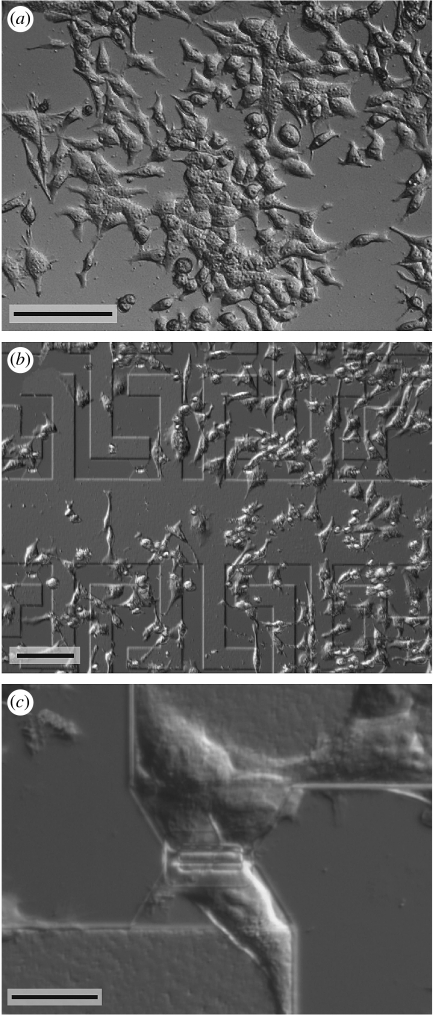
We used substrates with surface properties similar to those of our FET recording devices: 5 mm×5 mm pieces of smooth silicon (figure 1a) from the border of a wafer used in the FET fabrication, as well as FET chips (figure 1b). A thin layer of SiO2, on which the cells were growing, was the final passivation layer for all substrates. For details of the chip processing see Offenhäusser et al. (1997), Sprössler et al. (1998) and Ingebrandt et al. (2003).
Figure 1.
Differential interference contrast (DIC) images of HEK293 cells grown for 4 days on a poly(l)lysine-coated (a) smooth SiO2 surface, (b) a FET chip and (c) a single FET gate. Scale bars, (a,b) 50 μm and (c) 20 μm.
Before cell culturing, the substrates were cleaned as previously described (Wrobel et al. 2005) and coated with 25 μl of different protein solutions at room temperature for 30 min: (i) 0.05 mg ml−1 poly(l)lysine (PLL, molecular weight (MW): 150–300 kDa) in bi-distilled water, (ii) 0.1 mg ml−1 poly(d)lysine (PDL, MW: 30–70 kDa) in phosphate buffer solution (PBS) buffer (in mM: 137 NaCl, 2.7 KCl, 8.1 Na2HPO4, 1.5 KH2PO4, pH 7.3), (iii) 1% extracellular matrix gel (ECM) and 0.01 mg ml−1 PDL in Hanks' balanced salt solution (Invitrogen, Germany), (iv) 12.5 μg ml−1 fibronectin (FIB, MW: 450 kDa) in PBS buffer, (v) 0.1 mg ml−1 concanavalin-A (Con-A, MW: 104 kDa) in bi-distilled water, and (vi) 2 μg ml−1 laminin (LAM, MW: 900 kDa, all from Sigma, Germany) in a buffer solution (in mM: 150 NaCl, 50 Tris/HCl, pH 7.5). During this time, the proteins were allowed to adsorb onto the SiO2 surfaces. Before plating the cells, all surfaces were rinsed with PBS buffer in order to remove non-adsorbed proteins. As a control, we used similarly treated substrates without any protein coating.
2.2 Cell culture
We cultured HEK cells that expressed a voltage-gated K+ channel as previously described (Wrobel et al. 2005). In short, the cells were grown in minimal essential medium (M2279, Sigma), supplemented with 2 mM glutamine, 1% non-essential amino acids, 10% FBS, 100 units ml−1 penicillin and 0.1 mg ml−1 streptomycin (all from Invitrogen). The cells were plated onto the substrates at densities of 40–200 cells mm−2 and kept for 3–5 days at 37°C and 5% CO2. Figure 1 shows light microscopic images of HEK cells grown for 4 days on a PLL-coated smooth substrate (a) and on a FET chip (b,c).
2.3 Specimen preparation for transmission electron microscopy
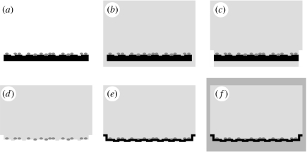
The attached cells were fixed with 3% glutaraldehyde (Serva, Germany) in 20 mM HEPES buffer (Carl Roth, Germany, pH 7.3 with NaOH) for 3 h. After washing in ultrapure water (Milli-Q Gradient A10 18.2 MΩ, Millipore Inc., Germany) (2×10 min), the cells were postfixed with 1% OsO4 (Next Chimica, RSA) in 20 mM HEPES buffer for 1 h. The cells were washed with ultrapure water (2×3 min), incubated with 2% uranyl acetate (Merck, Germany) for 2 h and then washed with ultrapure water (2×30 min). Following dehydration with a graded acetone series (20, 40, 60, 80 and 2×100%, each for 30 min), the specimens were incubated for 2×1 h with 100% propylene oxide (J. T. Baker, Netherlands; figure 2a). The specimens were then embedded in Spurr's epoxy resin (Spurr 1969; figure 2b): 23.6% ERL-4206; 14.2% D. E. R. 736; 61.3% nonenyl succinic anhydride (all from Ted Pella, Canada); and 0.9% dimethylaminoethanol (Plano, Germany). The specimens were transferred in 50% propylene oxide and 50% epoxy resin for 12 h. All steps were done at room temperature. The propylene oxide evaporated and the substrates were incubated in fresh epoxy resin (2×2 h) and polymerized at 70°C for 12 h.
Figure 2.
Flow chart of the specimen preparation. (a) The cells were fixed, stained and dehydrated. (b) Substrate and cells were embedded in an epoxy resin. (c,d) The silicon substrate was removed and (e) the former surface was contrasted by sputtering a gold or platinum/coal layer. (f) For structure preservation, the whole object was re-embedded in epoxy resin. TEM micrographs of ultrathin sections vertical to the surface were taken.
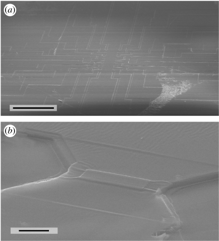
We removed the substrates by liquid N2 freeze fracture followed by sonication, because ultrathin sections of cells grown on the rigid silicon substrates (thickness: 500 μm) cannot be prepared. The cells remained in the epoxy resin and the interface became uncovered (figure 2c,d). We preserved that interface by sputtering a thin gold or platinum/coal layer onto the surface (SCD004, Balzers, Liechtenstein; figure 2e). In scanning electron microscopy pictures of these interfaces, one can clearly identify well-preserved imprints of the contact lanes and gates of a FET chip (figure 3).
Figure 3.
Typical scanning electron microscope images of platinum/coal-sputtered epoxy imprints of the FET surface and one single FET gate after the mechanical removal of the chip. One can clearly identify the well-preserved imprints of the contact lanes and gates of a FET chip. Scale bars, (a) 500 μm and (b) 10 μm.
The specimens were then re-embedded in epoxy resin (figure 2f) and polymerized for 12 h at 70°C. Thin sections (approx. 70 nm) were cut by an ultracut microtome (Reichert-Jung, Germany). The sections were collected on TEM copper grids, post-stained with 0.4% lead citrate (Agar Scientific, UK) in 0.4% NaOH for 4–10 min and rinsed with ultrapure water. The TEM images of these sections were taken with an EM902 transmission electron microscope (Zeiss, Germany) using a SIS Megaview II camera (Soft Imaging System, Germany) at resolutions up to 2.2 nm pixel−1. The images were further processed (contrast enhancement) using standard imaging software.
2.4 Surface characterization by imaging ellipsometry
Surfaces of the silicon substrates were characterized by IE, which allows determination of the layer thickness of the different protein coatings required for a detailed characterization of the cell–substrate distance. In addition, this method was used to determine the exact cleavage plane of the cell–substrate interface during the freeze fracture process in order to correct the distance values obtained from the TEM analysis. This cleavage could occur at different positions: at the SiO2–protein contact; within the adsorbed protein layers; or at the protein–cell contact. In order to get detailed information about the average position of this cleavage and possible differences between the coatings, we performed IE of the substrate surfaces using a multi-angle imaging ellipsometer (EP3, Nanofilm Technology, Germany, with a frequency doubled Nd:YAG laser (532 nm), lateral resolution 2 μm). The layer thickness was obtained as an average value (±s.d.) of n=20–40 different surface areas (10×10 μm2 to 25×25 μm2). The thickness fitting was done with the EP3 view software (nanofilm technology). We used the following refractive indices (Lide & Milne 1994): 4.1562 (Si) and 1.4605 (SiO2). The refractive indices reported for adsorbed protein layers typically range between 1.35 and 1.6 for ellipsometry and surface plasmon resonance data analysis (Jung et al. 1998; Benesch et al. 2002; Voros 2004). For simplification, we used in our study the refractive index of SiO2 for all proteins, which causes a smaller error compared with the large statistical variation of the IE thickness determination due to lateral variation of the protein layer thickness. For the IE data analysis, protein films were assumed to form homogeneous layers.
For this purpose, protein layers were deposited on silicon substrates with native SiO2. We determined twice the thickness of the protein layers: first, after the dehydration step; and second, after the freeze fracture. The thickness of the protein layers was calculated from differences against the non-coated substrate. In addition, we calculated the cleaved layer thickness by a comparison of the thickness value before and after freeze fracture.
3. Results
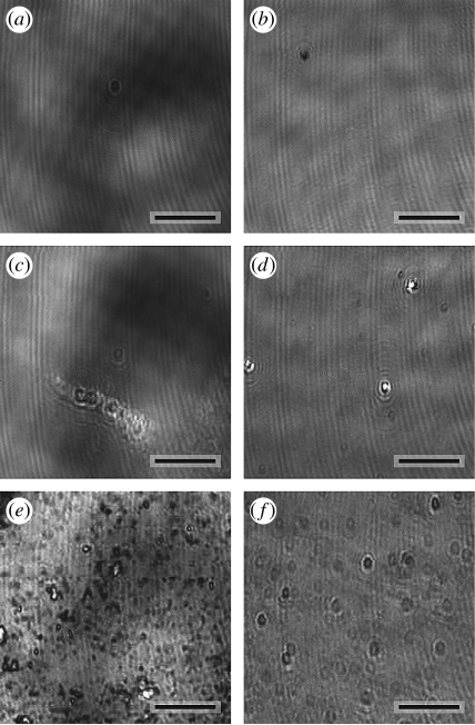
Figure 4 shows a comparison of ellipsometry images of the protein-coated silicon oxide surfaces before embedding into the epoxy resin and after freeze fracture. It can clearly be seen that the coating with the ECM protein mixture led to the most non-uniform surface. The SiO2 layer on the control substrates was 8.0±0.2 nm thick (table 1). The dehydrated protein films on the Si/SiO2 substrates showed layer thickness between 1.2 and 5.5 nm. After the embedding procedure and consecutive freeze fracture, these values decreased. For all surfaces except ECM, we found a remaining layer thickness (SiO2 and protein) of 6.8–8.8 nm, indicating the complete cleavage of the protein layers. In the case of the ECM-coated surfaces, it seemed that parts of the protein layer remained on the substrate surface. By a comparison of the thicknesses before and after specimen preparation, the cleaved protein layer thicknesses can be calculated to 2.2–4.0 nm (table 1). Local inhomogeneities in the layers with sub-micrometre resolution could not be accessed with this method.
Figure 4.
Comparison of ellipsometry images. The proteins were deposited on the smooth substrates, and IE of the substrates was performed (a,c,e) before embedding in the epoxy resin and (b,d,f) after the freeze fracture. (a,b: control; c,d: PLL, e,f: ECM). Scale bars, 10 μm.
Table 1.
Comparison of the layer thicknesses on the different precoated substrates before embedding in the epoxy resin and after the freeze fracture measured with IE. (The layer thickness of the control (8 nm) corresponded to the thickness of the SiO2 on top of the substrates. The errors for the thickness values were obtained from n=5–10 different areas (area size: 10×10 μm2 to 25×25 μm2) and four independent substrates for each layer preparation.)
| substrate coating | PLL | PDL | ECM | FIB | Con-A | LAM | control |
|---|---|---|---|---|---|---|---|
| total layer thickness before embedding (nm) | 11.3±2.3 | 11.1±1.9 | 13.5±3.7 | 12.6±1.9 | 11.0±0.8 | 9.2±0.4 | 8.0±0.2 |
| protein layer thickness (nm) | 3.3±2.3 | 3.1±1.9 | 5.5±3.7 | 4.6±1.9 | 3.0±0.8 | 1.2±0.4 | 0 |
| total layer thickness after freeze fracture (nm) | 7.3±0.5 | 7.9±0.8 | 12.0±0.7 | 8.8±0.5 | 8.8±0.2 | 6.8±0.2 | 8.5±0.1 |
| cleaved layer thickness (nm) | 4.0±2.6 | 3.2±2.1 | 1.5±3.8 | 3.8±2.0 | 2.2±0.8 | 2.4±0.4 | −0.5±0.2 |
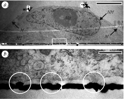
The detailed TEM study provided clear differences for the ultrathin sections of HEK cells grown on the protein coatings. Figure 5a shows a typical TEM image of a cell grown for 4 days on a PLL-coated smooth substrate. We found no distinct shrinking artefacts, and the whole cross section and prominent cellular structures were well preserved: the membrane (M); the nucleus (N) with the nucleolus (Nu); the nuclear membrane (NM); and mitochondria (Mi). The cell attached tightly to the substrate surface, which is marked by the sputtered layer (black line). Although the specimen was mechanically stressed while uncovering the cell–substrate interface, the surface morphology was only marginally affected. Small defects became visible by a partially slight roughness of the sputtered layer and by small gaps in this layer (figure 5a,b: white gaps).
Figure 5.
Typical TEM images of HEK cells grown on smooth substrates. (a) This image shows a HEK cell grown for 4 days on a PLL-coated substrate and (b) in higher magnification (white rectangle in (a)). The cell and prominent cellular structures were well preserved: membrane (M); nucleus (N) with nucleolus (Nu); nuclear membrane (NM); and mitochondria (Mi). The cell attached tightly to the substrate surface, which is marked by the gold-sputtered layer (black line). Differences were found in the membrane attachment: areas of close adhesion (white circles) and areas with enhanced distance. Scale bars, (a) 5 μm, (b) 1 μm.
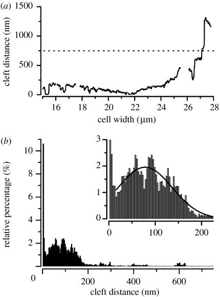
We could clearly distinguish between areas where the membrane attached tightly to the surface and areas with an increased cleft distance. In all preparations, dj increased to the boundaries of the attached cell (figure 5a, right border). Higher magnification of a part of this interface showed the differences in the membrane attachment in detail (b): areas of close adhesion with dj≤10 nm (white circles) and areas with enhanced distance of 100–150 nm in this particular case.
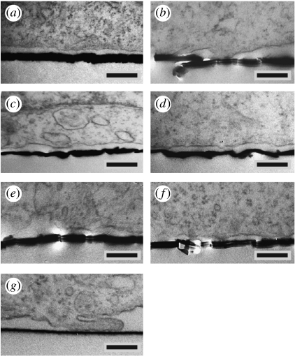
Next, the influence of the different protein coatings on the geometry of the cell–substrate interface was characterized using TEM (figure 6). Again, the cells and subcellular structures were optimally preserved, and we found no homogeneous distance for the cell–substrate interface. These experiments, however, also provide differences in the quality of the interface preparation: we found not only flat (a: PLL, g: control) or partially rough, sputtered metal layers (c: ECM, d: FIB) but also cutting artefacts (b: PDL, e: LAM, f: Con-A). However, similar to the integrative nature of the IE data, the TEM study can reveal differences in the protein layers from a statistical analysis of many cross sections.
Figure 6.
Typical TEM images of HEK cells grown on different protein-coated smooth substrates: (a) PLL, (b) PDL, (c) ECM, (d) FIB, (e) LAM, (f) Con-A and (g) non-coated control. Scale bars, 250 nm.
The TEM images were further analysed using a procedure described in detail in the following part for figure 5a: figure 7a depicts the changes in dj of this cell. The intersections in this graph correspond to the gaps in the sputtered layer. Figure 7b shows the corresponding histogram of the distance distribution, while the inset of this figure shows a part of the histogram in a higher magnification. We neglected the values of dj>750 nm for the distance histogram (see appendix A). Two preferential distributions in this histogram were obtained: first, dj=0–10 nm, which corresponds to the close membrane adhesion; and second, dj=10–200 nm, with a maximum around 50–100 nm. We found a fraction of 14% of the total attached membrane in the first distance range and a larger fraction of 77% in the second range. Larger values of dj were also found, but can be attributed to the cell boundary in this case (figure 7a). We fitted the left part of the histogram by a Gaussian distribution (inset in figure 7b, black curve) and obtained an average cleft distance of for this exemplary TEM image. To facilitate a better comparison between the different substrate coatings, we defined the d90 value as the distance within which 90% of the attached membrane can be found. For this particular TEM image, we obtained a d90 value of 178 nm.
Figure 7.
(a) This diagram shows the cleft distance dj of the TEM image in figure 5a in dependence on the cell width. We could clearly distinguish between close adhesion of the membranes with dj≤10 nm, enhanced distances of dj=100–150 nm and distances dj≥500 nm at the border of cell–substrate interface. The intersections in the trace correspond to the gaps in the sputtered layer (white gaps in figure 5a,b). (b) Distance distribution for the cell–surface distance of the cell shown in figure 5a. We neglected distance values of dj≥750 nm (dotted line in (a)) as we found them only at the borders of cell–substrate interface. The inset shows a part of the histogram at higher magnification. We fitted the data to a Gaussian distribution (inset, black curve) and obtained an average cleft distance of .
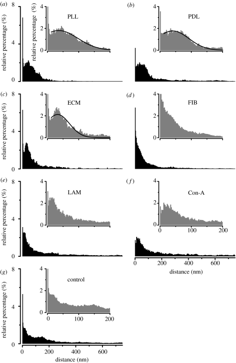
Using this procedure for a number of TEM images, a comparison between the different surface coatings was realized. Figure 8 shows the cumulative distance distribution histograms for n=5–15 cells on the different protein-coated surfaces. The insets show parts of the respective histograms in higher magnification. A first observation was that the close membrane adhesion was only weakly correlated with the type of protein coating. In all cases, we found 5–20% of the cell membrane tightly attached at dj=0–10 nm (table 2). The cumulative histograms for the cells on the polylysine-coated surfaces (figure 8a: PLL, b: PDL, c: ECM) were similar to the single histogram in figure 7b. We obtained an average cleft distance of (PLL), 41 nm (PDL) and 33 nm (ECM), by fitting the data to Gaussians (black curves). For the other coatings, the cumulative histograms differed significantly—the histogram for cells on FIB resembled an exponential decay (d). For LAM (e) and Con-A (f) the data were comparable, and we observed a significant reduction of the close adhesion. For the non-coated surfaces (g), we found no preferred cleft distance and a large amount of areas of larger distance (100–200 nm).
Figure 8.
Cumulative histograms of the distance distribution for n=5–15 HEK cells grown on smooth surfaces with different protein coatings. In all cases, 10–20% of the attached membrane showed close adhesion with distances of dj≤10 nm. By fitting the histograms for the cells on polylysine-coated surfaces to Gaussians (a–c, black curves), we obtained average cleft distances of (PLL), 41 nm (PDL) and 33 nm (ECM). For the other substrate coatings (d–g) we found no comparable distance distribution.
Table 2.
Comparison of the percentage of membrane attachment for different protein coatings for close adhesion (dj≤10 nm), and distances of dj=10–100 nm. (For better comparison of the cell attachment, we defined the distance range for 90% of the attached membrane as the ‘d90 value’. This table summarizes the cumulated distance distribution histograms for n=5–15 HEK cells shown in figure 8.)
| substrate coating | PLL | PDL | ECM | FIB | Con-A | LAM | control |
|---|---|---|---|---|---|---|---|
| fraction of membrane for dj≤10 nm | 14.0% | 9.7% | 14.1% | 20.6% | 11.8% | 6.9% | 12.6% |
| fraction of membrane for dj=10–100 nm | 78.7% | 72.7% | 76.9% | 77.1% | 59.4% | 53.9% | 49.9% |
| 90% of membrane area within dj=x nm | 130 nm | 235 nm | 201 nm | 197 nm | 391 nm | 444 nm | 411 nm |
| average cleft distance | 37 nm | 41 nm | 33 nm | — | — | — | — |
The data extracted from the cumulative histograms shown in figure 8 are summarized in table 2: one can clearly see that PLL, PDL, ECM and FIB coatings lead to a closer adhesion of cells compared with LAM, Con-A and no coating. For Con-A, the amount of close adhesion was significantly reduced. The best coating was PLL with the lowest d90 value (130 nm) and the highest amount of membrane distances between 10 and 100 nm (78.7%). Owing to the different histogram shape, FIB had a lower d90 value (197 nm) and the highest value of close adhesion of all coatings (20.6%).
4. Discussion
We cultured HEK293 cells on smooth silicon substrates, which were coated with different protein types, and analysed the distance of the cell–substrate interface by a statistical TEM analysis of ultrathin sections. As a summary for all TEM images, we made the following key observations: first, distinct areas of the membrane attached tightly to the surfaces and the amount of this close adhesion areas was only weakly correlated to the type of protein coating. For the FIB coating, we found the highest value of close adhesion area. Second, the adhesion of the cells to polylysine-containing coatings (PLL, PDL, ECM) was dominated by an average cleft distance of . For the other coatings, we found no preferred distance range.
A corresponding IE study of the substrate surfaces revealed the following main results. The average protein layer thicknesses were measured to 1.2–5.5 nm with LAM being the thinnest and ECM the thickest protein layer. The large statistical errors of the IE thickness data reflect the local inhomogeneities underlying all protein coatings. After embedding of the substrates in epoxy resin and subsequent freeze fracture, the IE study of the cleaved SiO2 surfaces revealed that for almost all coatings the main fraction of the deposited protein material remained inside of the epoxy resin. Only for the ECM-coated surface, a distinct amount of protein was still present at the substrate surface and large inhomogeneities were visible. It is highly probable that these local inhomogeneities were partly responsible for the non-uniform metal interfaces in the TEM images. However, due to the statistical analysis of many TEM sections in our study, these local variations will not affect the average values when comparing different coatings. Nevertheless, the thickness values for the TEM data need to be corrected by the thickness of the respective protein coating, since these values add to the distance values extracted from the TEM images.
As a general remark to the IE study, a comparison of the errors underlying the TEM and the IE analysis is appropriate. A single pixel in the TEM images corresponded to 2.2 nm. Consequently, all thickness values and errors from the IE study correspond to an error of ±2 pixels for the graphical evaluation of the TEM images. Therefore, we conclude that the errors while analysing the TEM images will mainly contribute to the overall error underlying this cell–substrate distance analysis.
In our TEM study, we found different effects of the various protein coatings on the cell attachment: in all cases, 5–20% of the attached membrane showed close adhesion to the surfaces with distances of dj≤10 nm. It is accepted that this close adhesion is correlated with focal adhesion points of the cells (Chen & Singer 1982; Matsuzaka et al. 2003). Thus, we assume that the areas of close adhesion represented focal adhesion points of the cells, as to be seen in the membrane protrusions in figure 5b. For the remaining membrane areas in the cell–substrate interface, we found a different situation. In the presence of polylysine (PLL, PDL and ECM) or FIB, a large fraction of the attached membrane had distances of dj≤100 nm. For Con-A, LAM and the non-coated surfaces, we found only a weaker cell adhesion with a significant reduction of close adhesion for Con-A. From these results, we conclude that the precoating with polylysine or FIB enhanced the cell attachment to the substrate surface, whereas the other coatings were not suited for tight cell attachment.
Our results for the average cleft distance values (table 2) are in good accordance with the previously published distances of mammalian cells on microstructured and protein-coated silicon dioxide surfaces, which were obtained by FLIC microscopy (Braun & Fromherz 1998; Iwanaga et al. 2001; Lambacher & Fromherz 2002). The cleft distance of HEK293 cells on different proteins was previously studied by FLIC microscopy: 55±10 nm for collagen (Straub et al. 2001), and 70±10 and 75±1 nm, respectively, for FIB (Brittinger & Fromherz 2005; Gleixner & Fromherz 2006). In the respective studies, the main findings were similar to the results in our TEM studies. First, the presence of polylysine or FIB led to enhanced cell adhesion, and second, also inhomogeneities in the distance distribution of attached cells were found.
Especially for the latter finding, our TEM studies add further details. This method allows one to precisely follow the cell–sensor topography with a lateral and vertical resolution of 2.2 nm. In addition, one can get a better insight into the modelling of the cell–sensor interface. The major challenges of the TEM method compared with the optical methods, however, are the complicated and time-consuming preparation of the cross-sectional samples, the need to fix the cells and the low total area which can be accessed for statistical analysis. In a recent work, Heeren et al. (2006) introduced an approach to overcome the difficulties of conventional ultrathin sectioning using a focused ion beam technique for cutting lamellae of embedded cells grown on titanium substrates. Subsequently, the lamellae can be analysed by scanning electron microscopy or the TEM technique.
In our study, local variations in the sputtered metal layers, cutting artefacts and the graphical analysis of the TEM images decrease the resolution of the distance data. Moreover, owing to the delicate microtome preparation, it was almost impossible to collect several sections from one and the same cell. Therefore, we were not able to obtain a complete reconstruction of a single cell–substrate interface region. For all these reasons, the presented TEM method should be seen as complementary to the commonly used optical methods.
5. Conlcusions
In the present work, we analysed the cleft distance between HEK cells and substrate surfaces, which were comparable to that of our extracellular recording FET devices. As we observed variations in the cell–substrate distance for different protein coatings, we also expect differences in the electrical seal resistance and consequently in the electronic coupling strength for cells growing on different precoated FETs. Future work will focus on the correlation of the d90 values of the HEK cells and the electronic coupling strength of extracellular recordings.
Acknowledgments
The authors sincerely thank R. Stockmann for the fabrication of the FET chips, and R. Helpenstein (both IBN-2) for help with the cell culture. They also thank A. Baumann (IBI-1, all Forschungszentrum Jülich) for providing them with the HEK293 cells with the beag1 gene.
Appendix A.
We determined the distance dj of the cleft between attached cell membranes and the smooth substrates in dependence on the respective protein coating. Therefore, we took a series of high-resolution TEM images of the cell–substrate interface similar to the TEM image shown in figure 5b. We manually traced the cellular membrane and the upper side of the sputtered metal layer with a line (thickness: 1 pixel) using standard imaging software. Gaps in the sputtered layer were excluded for the statistics (white gaps in figure 6a,b). The lines were exported as an image file, and we determined the amount of pixels between both lines and consequently the cleft distance using a Matlab v. 5.2 (The Mathworks, USA) routine at a lateral and vertical resolution of 2.2 nm pixel−1. We chose distinct boundary conditions for the Matlab routine and neglected values of dj >750 nm. This value seemed to be appropriate, as we only found these distances at the boundaries of the cell attachment (figures 6a and 7a).
References
- Axelrod D. Cell–substrate contacts illuminated by total internal-reflection fluorescence. J. Cell Biol. 1981;89:141–145. doi: 10.1083/jcb.89.1.141. [DOI] [PMC free article] [PubMed] [Google Scholar]
- Baharloo B, Textor M, Brunette D.M. Substratum roughness alters the growth, area, and focal adhesions of epithelial cells, and their proximity to titanium surfaces. J. Biomed. Mater. Res. A. 2005;74A:12–22. doi: 10.1002/jbm.a.30321. [DOI] [PubMed] [Google Scholar]
- Benesch J, Askendal A, Tengvall P. The determination of thickness and surface mass density of mesothick immunoprecipitate layers by null ellipsometry and protein 125iodine labeling. J. Colloid Interf. Sci. 2002;249:84–90. doi: 10.1006/jcis.2002.8247. [DOI] [PubMed] [Google Scholar]
- Bergveld P, Wiersma J, Meertens H. Extracellular potential recordings by means of a field-effect transistor without gate metal, called Osfet. IEEE Trans. Biomed. Eng. 1976;23:136–144. doi: 10.1109/TBME.1976.324574. [DOI] [PubMed] [Google Scholar]
- Braun D, Fromherz P. Fluorescence interferometry of neuronal cell adhesion on microstructured silicon. Phys. Rev. Lett. 1998;81:5241–5244. doi: 10.1103/PhysRevLett.81.5241. [DOI] [Google Scholar]
- Brittinger M, Fromherz P. Field-effect transistor with recombinant potassium channels: fast and slow response by electrical and chemical interactions. Appl. Phys. A. 2005;81:439–447. doi: 10.1007/s00339-005-3272-7. [DOI] [Google Scholar]
- Chen W.T, Singer S.J. Immunoelectron microscopic studies of the sites of cell–substratum and cell–cell contacts in cultured fibroblasts. J. Cell Biol. 1982;95:205–222. doi: 10.1083/jcb.95.1.205. [DOI] [PMC free article] [PubMed] [Google Scholar]
- Curtis A.S.G. Mechanism of adhesion of cells to glass—study by interference reflection microscopy. J. Cell Biol. 1964;20:199–215. doi: 10.1083/jcb.20.2.199. [DOI] [PMC free article] [PubMed] [Google Scholar]
- den Braber E.T, Jansen H.V, de Boer M.J, Croes H.J.E, Elwenspoek M, Ginsel L.A, Jansen J.A. Scanning electron microscopic, transmission electron microscopic, and confocal laser scanning microscopic observation of fibroblasts cultured on microgrooved surfaces of bulk titanium substrata. J. Biomed. Mater. Res. 1998;40:425–433. doi: 10.1002/(SICI)1097-4636(19980605)40:3%3C425::AID-JBM13%3E3.0.CO;2-I. [DOI] [PubMed] [Google Scholar]
- Fromherz P, Offenhäusser A, Vetter T, Weis J. A neuron–silicon junction—a Retzius cell of the leech on an insulated-gate field-effect transistor. Science. 1991;252:1290–1293. doi: 10.1126/science.1925540. [DOI] [PubMed] [Google Scholar]
- Gingell D, Todd I, Bailey J. Topography of cell glass apposition revealed by total internal-reflection fluorescence of volume markers. J. Cell Biol. 1985;100:1334–1338. doi: 10.1083/jcb.100.4.1334. [DOI] [PMC free article] [PubMed] [Google Scholar]
- Gleixner R, Fromherz P. The extracellular electrical resistivity in cell adhesion. Biophys. J. 2006;90:2600–2611. doi: 10.1529/biophysj.105.072587. [DOI] [PMC free article] [PubMed] [Google Scholar]
- Gross G.W, Wen W.Y, Lin J.W. Transparent indium tin oxide electrode patterns for extracellular, multisite recording in neuronal cultures. J. Neurosci. Methods. 1985;15:243–252. doi: 10.1016/0165-0270(85)90105-0. [DOI] [PubMed] [Google Scholar]
- Heeren A, Burkhardt C, Wolburg H, Henschel W, Nisch W, Kern D.P. Preparation of nanostructured titanium surfaces for investigations of the interface between cell monolayers and titanium. Microelectron. Eng. 2006;83:1602–1604. doi: 10.1016/j.mee.2006.01.114. [DOI] [Google Scholar]
- Ingebrandt S, Yeung C.K, Staab W, Zetterer T, Offenhäusser A. Backside contacted field effect transistor array for extracellular signal recording. Biosens. Bioelectron. 2003;18:429–435. doi: 10.1016/S0956-5663(02)00155-0. [DOI] [PubMed] [Google Scholar]
- Ingebrandt S, Yeung C.K, Krause M, Offenhausser A. Neuron-transistor coupling: interpretation of individual extracellular recorded signals. Eur. Biophys. J. 2005;34:144–154. doi: 10.1007/s00249-004-0437-9. [DOI] [PubMed] [Google Scholar]
- Iwanaga Y, Braun D, Fromherz P. No correlation of focal contacts and close adhesion by comparing GFP-vinculin and fluorescence interference of Dil. Eur. Biophys. J. 2001;30:17–26. doi: 10.1007/s002490000119. [DOI] [PubMed] [Google Scholar]
- Izzard C.S, Lochner L.R. Cell-to-substrate contacts in living fibroblasts—interference reflection study with an evaluation of technique. J. Cell Sci. 1976;21:129–159. doi: 10.1242/jcs.21.1.129. [DOI] [PubMed] [Google Scholar]
- Jung L.S, Campbell C.T, Chinowsky T.M, Mar M.N, Yee S.S. Quantitative interpretation of the response of surface plasmon resonance sensors to adsorbed films. Langmuir. 1998;14:5636–5648. doi: 10.1021/la971228b. [DOI] [Google Scholar]
- Khakbaznejad A, Chehroudi B, Brunette D.M. Effects of titanium-coated micromachined grooved substrata on orienting layers of osteoblast-like cells and collagen fibers in culture. J. Biomed. Mater. Res. A. 2004;70A:206–218. doi: 10.1002/jbm.a.30058. [DOI] [PubMed] [Google Scholar]
- Lambacher A, Fromherz P. Fluorescence interference-contrast microscopy on oxidized silicon using a monomolecular dye layer. Appl. Phys. A. 1996;63:207–216. [Google Scholar]
- Lambacher A, Fromherz P. Luminescence of dye molecules on oxidized silicon and fluorescence interference contrast microscopy of biomembranes. J. Opt. Soc. Am. B. 2002;19:1435–1453. [Google Scholar]
- Lide D.R, Milne G.W.A. CRC Press; Boca-Raton, FL: 1994. CRC handbook of data on organic compounds. [Google Scholar]
- Matsuzaka K, Walboomers X.F, Yoshinari M, Inoue T, Jansen J.A. The attachment and growth behavior of osteoblast-like cells on microtextured surfaces. Biomaterials. 2003;24:2711–2719. doi: 10.1016/S0142-9612(03)00085-1. [DOI] [PubMed] [Google Scholar]
- Meyburg S, Wrobel G, Stockmann R, Moers J, Ingebrandt S, Offenhäusser A. Single cell recordings with pairs of complementary transistors. Appl. Phys. Lett. 2006;89:013 901. doi: 10.1063/1.2219339. [DOI] [Google Scholar]
- Meyle J, Gultig K, Wolburg H, Von Recum A.F. Fibroblast anchorage to microtextured surfaces. J. Biomed. Mater. Res. 1993;27:1553–1557. doi: 10.1002/jbm.820271212. [DOI] [PubMed] [Google Scholar]
- Offenhäusser A, Sprössler C, Matsuzawa M, Knoll W. Field-effect transistor array for monitoring electrical activity from mammalian neurons in culture. Biosens. Bioelectron. 1997;12:819–826. doi: 10.1016/S0956-5663(97)00047-X. [DOI] [PubMed] [Google Scholar]
- Pabst, M., Wrobel, G., Ingebrandt, S., Sommerhage, F. & Offenhäusser, A. Submitted. Solution of the Poisson–Nernst–Planck equations in the cell–substrate interface. [DOI] [PubMed]
- Pfeiffer F, Herzog B, Kern D, Scheideler L, Geis-Gerstorfer J, Wolburg H. Cell reactions to microstructured implant surfaces. Microelectron. Eng. 2003;67-8:913–922. doi: 10.1016/S0167-9317(03)00154-0. [DOI] [Google Scholar]
- Pine J. Recording action-potentials from cultured neurons with extracellular micro-circuit electrodes. J. Neurosci. Methods. 1980;2:19–31. doi: 10.1016/0165-0270(80)90042-4. [DOI] [PubMed] [Google Scholar]
- Regehr W.G, Pine J, Cohan C.S, Mischke M.D, Tank D.W. Sealing cultured invertebrate neurons to embedded dish electrodes facilitates long-term stimulation and recording. J. Neurosci. Methods. 1989;30:91–106. doi: 10.1016/0165-0270(89)90055-1. [DOI] [PubMed] [Google Scholar]
- Schätzthauer R, Fromherz P. Neuron–silicon junction with voltage-gated ionic currents. Eur. J. Neurosci. 1998;10:1956–1962. doi: 10.1046/j.1460-9568.1998.00205.x. [DOI] [PubMed] [Google Scholar]
- Singhvi R, Stephanopoulos G, Wang D.I.C. Effects of substratum morphology on cell physiology—review. Biotechnol. Bioeng. 1994;43:764–771. doi: 10.1002/bit.260430811. [DOI] [PubMed] [Google Scholar]
- Sprössler C, Richter D, Denyer M, Offenhäusser A. Long-term recording system based on field-effect transistor arrays for monitoring electrogenic cells in culture. Biosens. Bioelectron. 1998;13:613–618. doi: 10.1016/S0956-5663(98)00016-5. [DOI] [Google Scholar]
- Sprössler C, Denyer M, Britland S, Curtis A, Knoll W, Offenhäusser A. Electrical recordings from rat cardiac muscle cells using field-effect transistors. Phys. Rev. E. 1999;60:2171–2176. doi: 10.1103/PhysRevE.60.2171. [DOI] [PubMed] [Google Scholar]
- Spurr A.R. A low-viscosity epoxy resin embedding medium for electron microscopy. J. Ultra. Res. 1969;26:31–43. doi: 10.1016/S0022-5320(69)90033-1. [DOI] [PubMed] [Google Scholar]
- Straub B, Meyer E, Fromherz P. Recombinant maxi-K channels on transistor, a prototype of iono-electronic interfacing. Nat. Biotechnol. 2001;19:121–124. doi: 10.1038/84369. [DOI] [PubMed] [Google Scholar]
- Voros J. The density and refractive index of adsorbing protein layers. Biophys. J. 2004;87:553–561. doi: 10.1529/biophysj.103.030072. [DOI] [PMC free article] [PubMed] [Google Scholar]
- Walboomers X.F, Croes H.J.E, Ginsel L.A, Jansen J.A. Growth behavior of fibroblasts on microgrooved polystyrene. Biomaterials. 1998;19:1861–1868. doi: 10.1016/S0142-9612(98)00093-3. [DOI] [PubMed] [Google Scholar]
- Weis R, Fromherz P. Frequency dependent signal-transfer in neuron-transistors. Phys. Rev. E. 1997;55:877–889. doi: 10.1103/PhysRevE.55.877. [DOI] [Google Scholar]
- Weis R, Muller B, Fromherz P. Neuron adhesion on a silicon chip probed by an array of fieldeffect transistors. Phys. Rev. Lett. 1996;76:327–330. doi: 10.1103/PhysRevLett.76.327. [DOI] [PubMed] [Google Scholar]
- Wrobel G, Seifert R, Ingebrandt S, Enderlein J, Ecken H, Baumann A, Kaupp U.B, Offenhäusser A. Cell-transistor coupling: investigation of potassium currents recorded with p- and n-channel FETs. Biophys. J. 2005;89:3628–3638. doi: 10.1529/biophysj.104.049809. [DOI] [PMC free article] [PubMed] [Google Scholar]


