

Abstract
A Monte Carlo electron-trajectory calculation has been implemented to assess the optimal detector configuration for scanning transmission electron microscopy (STEM) tomography of thick biological sections. By modeling specimens containing 2 and 3 atomic % osmium in a carbon matrix, it was found that for 1-μm thick samples the bright-field (BF) and annular dark-field (ADF) signals give similar contrast and signal-to-noise ratio provided the ADF inner angle and BF outer angle are chosen optimally. Spatial resolution in STEM imaging of thick sections is compromised by multiple elastic scattering which results in a spread of scattering angles and thus a spread in lateral distances of the electrons leaving the bottom surface. However, the simulations reveal that a large fraction of these multiply scattered electrons are excluded from the BF detector, which results in higher spatial resolution in BF than in high-angle ADF images for objects situated towards the bottom of the sample. The calculations imply that STEM electron tomography of thick sections should be performed using a BF rather than an ADF detector. This advantage was verified by recording simultaneous BF and high-angle ADF-STEM tomographic tilt series from a stained 600-nm thick section of C. elegans. It was found that loss of spatial resolution occurred markedly at the bottom surface of the specimen in the ADF-STEM but significantly less in the BF-STEM tomographic reconstruction. Our results indicate that it might be feasible to use BF-STEM tomography to determine the 3D structure of whole eukaryotic microorganisms prepared by freeze-substitution, embedding, and sectioning.
Keywords: Scanning transmission electron microscopy, STEM, electron tomography, Monte Carlo simulation, thick sections
Introduction
In electron tomography (ET), the three-dimensional structure of a cell is typically derived from a series of bright-field images that are collected over a range of tilt angles in a transmission electron microscope (TEM) [1-3]. Electron tomography is often applied to tissues or isolated cells that have been rapidly frozen, freeze-substituted at low temperature in a solvent to remove water, embedded in a polymer resin, sectioned and stained to visualize structures of interest. The highest resolution of reconstructed cellular volumes is obtained from the thinnest sections (30-100 nm) [4-5]. However, there is also an interest in imaging sections with a thickness of around 1 μm, albeit at a lower resolution [6].
Currently, in order to visualize large cellular structures or entire cells it is necessary to record tomographic volumes of thin slabs prepared by serial sectioning on an ultramicrotome [7-9]. The full 3D volume is recreated by aligning and stacking the tomograms obtained from each serial section, a process which is computationally intensive. The ability to perform tomography on micron-thick specimens would significantly reduce the number of serial sections required to cover a large volume of cellular material. It would also enable visualization of whole cellular organelles or eukaryotic microorganisms like Ostreococcus tauri [10] that can be contained within a single thick section.
When conventional ET performed with unfiltered bright field imaging in a TEM is applied to micrometer thick sections, the resulting tomographic reconstruction yields very poor spatial resolution. This is because the incident electrons undergo multiple inelastic scattering events producing a range of energy losses, so that the transmitted electrons are focused at different imaging planes due to chromatic aberration of the objective lens [11-12]. One way to circumvent this problem is to utilize only electrons with a narrow energy window (e.g. 30 eV) for image formation. This approach was successfully implemented by Bouwer et al. through an automated most-probable energy-loss tomography technique [6]. In thick sections, the largest signal is obtained by using an energy band at the intensity maximum in the energy-loss spectrum (i.e., the most probable energy loss). Another approach for imaging thick sections – based on exit wavefront reconstruction from a few focus levels – has also been proposed [13,14].
The scanning transmission electron microscope (STEM) provides an alternative approach for electron tomography of thick biological specimens [15,16]. STEM tomography has already been shown to be a promising technique for determining the 3D ultrastructure of thin stained biological sections [17] as well as for locating in 3D heavy-metal nanoparticles that label specific cellular proteins [18-20]. In STEM there are no image-forming lenses after the specimen, so the spatial resolution in images of thick specimens is not degraded by chromatic aberration. On the other hand, STEM tomography of thick sections is compromised by the incident probe convergence semi-angle, which is typically of the order of 10 mrad. Therefore, on the basis of geometrical considerations only, a probe focused on top of a 1 μm-thick specimen would extend to a diameter of 20 nm at the bottom surface. An adequate solution to this problem is to decrease the convergence angle of the illumination, e.g. down to approximately 2 mrad [21]. In addition to its potential use for the 3D imaging of thick biological sections, STEM tomography can be also applied to the 3D reconstruction of thick specimens in materials science [22]. The theory of STEM imaging and tomographic reconstruction for such specimens has been discussed in detail by Levine [23,24].
STEM imaging in a modern TEM/STEM microscope enables the use of several different schemes for signal detection. First, it is possible to acquire images with a bright-field (BF) detector as well as with an annular dark-field (ADF) detector. Second, for both these modes of detection, it is possible to select different ranges of collection angles. For thin specimens, ADF STEM is well known to be superior to BF STEM imaging in terms of both signal-to-noise ratio (SNR) and contrast. For specimens of moderate to large thicknesses, however, the optimum scheme for signal acquisition is unclear. In electron tomography, in particular, the increasing specimen thickness in the beam direction as a function of tilt angle makes it more challenging to predict how a given mode of STEM signal acquisition will influence the contrast, SNR and resolution of specimen features within a reconstructed tomogram.
Here we use Monte Carlo electron-trajectory simulations [25-27] to investigate the use of STEM for imaging plastic-embedded and stained biological specimens of various thicknesses. In the simulations, we determine how contrast, SNR and resolution vary according to the specific configuration of the STEM detection system. From experimental data, we confirm the trends outlined by the Monte Carlo simulations and show how choice of STEM detector configuration influences the quality of the 3D reconstruction of a plastic-embedded, semi-thick stained biological specimen.
Experimental
Monte Carlo simulation
Monte Carlo simulations have been previously used by several groups to investigate a wide range of phenomena in both transmission and scanning electron microscopy, including the spatial resolution in x-ray microanalysis, image blurring due to elastic and inelastic scattering, and ratio-contrast imaging for the quantification of plastic-embedded biological matter [28-31]. Our Monte Carlo simulation program is based on the algorithms outlined by Joy [25] and Hovington et al. [26]. Only elastic scattering events are taken into account in the simulations. Adding the contribution of inelastic events would entail only minor changes to the calculations and not affect the conclusions.
In a Monte Carlo simulation [25-27], an incident electron penetrates the specimen and travels by a random distance L (governed by Eq. 1 below) before being scattered elastically. At the point of collision of the fast electron with the specimen, the electron is deflected by a scattering angle θ (governed by Eq. 3 below) and a random azimuthal angle φ. The electron then travels an additional random distance L, is again deflected, and so on until it reaches the bottom surface of the specimen. Typically, the trajectories of hundreds of thousands of incident electrons must be computed to achieve a high degree of statistical precision. The random distance L is calculated according to the following expression:
| (1) |
Where, R1 is a floating-point random number uniformly distributed between 0 and 1, ρ is the density of the specimen, and σe is the total elastic scattering cross section characteristic of the specimen, defined as:
| (2) |
where is the differential elastic-scattering cross section for scattering angle θ per unit solid angle Ω. is a function of atomic number and incident beam energy.
For calculating σe in Eq. 2, we used values of from the Elastic-Scattering Cross-Section database of the National Institute of Standards and Technology (NIST) [32]. The NIST database was also utilized to calculate numerically the scattering angle θ of the electrons at each collision point within the specimen. This was accomplished by pre-calculating and storing in a lookup table values of R2 as a function of θ, according to the equation:
| (3) |
During the Monte Carlo simulations, the scattering angles θ were calculated by generating uniformly distributed random numbers R2 and finding the corresponding values of θ in the lookup table. The azimuthal angle of deflection of the electrons at each collision is straightforward to calculate, namely, φ = R2 · 2π.
In our Monte Carlo simulations, we modeled specimens consisting of Os atoms homogeneously distributed in carbon layers with thicknesses ranging from 200 to 4000 nm and density of 1 g/cm3. Specimens with two distinct compositions were modeled, namely, 2 and 3 atomic percent Os in C. For each simulation performed, the trajectories of 1 million incident electrons were computed. Fig. 1a shows an example Monte Carlo simulation, where an electron beam of 10 mrad convergence semi-angle was focused at the bottom surface of a 1 μm-thick specimen. For each incident electron, we determined its coordinate (x,y) as well as its net scattering angle θn at the bottom surface of the model specimens (Figs. 1b and 1c). BF and ADF STEM signals for detectors subtending various collection angles (Fig. 2) were computed using the values of θn stored for each electron. To evaluate the effect of multiple elastic scattering on beam broadening, we assumed the presence of a cluster of Os atoms at the bottom surface of the specimens. In this case, the angles θn represented the angles with which electrons impinged onto the cluster before being scattered by it. Contrast and SNR were determined from curves such as the ones displayed in Fig. 2. Values of contrast for a given collection angle of the ADF STEM detector were determined as C = (F3 − F2)/F2, where F3 and F2 represent the fraction of electrons collected from specimens of 3 and 2 atomic percent Os in C, respectively. Values of SNR were calculated as , where I0 is the incident number of electrons. C and SNR for BF STEM were calculated in an equivalent way: C = (F2 − F3)/F3 and . Calculation of SNR was performed by considering 10,000 incident electrons.
Fig. 1.
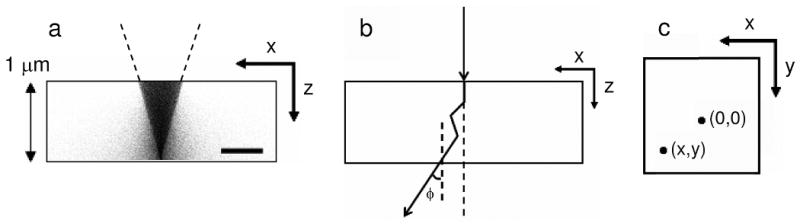
(a) Example Monte Carlo simulation showing electron trajectories inside a 1 μm-thick specimen consisting of 2 atomic percent Os in carbon. The incident probe had a 10 mrad convergence semi-angle and was focused at the bottom surface. Each dot in the image corresponds to a point of collision of the incident electrons. (b) Schematic diagram of the trajectory for a single incident electron inside the specimen. The electron scatters three times before arriving at the bottom surface displaced from the center and with a net scattering angle of θn. (c) Schematic representation showing the xy plane at the bottom surface of the specimen. The electron arrives at the bottom surface at the coordinate (x,y) displaced from the origin. Scale bar is 20 nm.
Fig. 2.

Fraction of the incident number of electrons collected by STEM detectors of different collection geometries as a function of specimen thickness. The closed and open symbols are for specimens of 3 at% Os-C and 2 at% Os-C, respectively. Triangles: BF STEM detector of 13 mrad outer semi-angle. Circles: ADF STEM detector with inner collection semi-angle of 16 mrad. Squares: ADF STEM detector with inner collection semi-angle of 40 mrad. The outer semi-angles of the ADF detectors are 5 times the inner angles. Contrast inversion occurs at around 2 μm for an ADF detector of small (e.g. 16 mrad) inner semi-angle.
STEM imaging and tomography
STEM imaging and tomography were performed using a Tecnai TF30 electron microscope (FEI, Hillsboro, OR, USA) operating at an acceleration voltage of 300 kV with a Shottky field-emission gun. This instrument is equipped with a high-efficiency Fischione ADF STEM detector (Fischione, Export, PA, USA) situated below the projection-lens system and above the viewing screen. This microscope is also equipped with a Gatan BF/ADF assembly (Gatan, Pleasanton, CA, USA) situated after the viewing screen.
We recorded BF and ADF STEM images of 20 nm-diameter gold particles located at the top and bottom surfaces of an approximately 1 μm-thick stained plastic section that was tilted to 60°, thus giving an effective specimen thickness in the beam direction of around 2 μm. The convergence semi-angle of the STEM probe on the specimen was 12 mrad. Gold particles located at the top surface of the specimen were imaged with the STEM probe focused precisely at the top surface. Likewise, the STEM probe was focused at the bottom surface when imaging gold particles situated there. The BF and ADF STEM signals were acquired simultaneously using the Gatan and Fischione detectors, respectively. BF imaging was accomplished with a 13 mrad detector outer semi-angle, whereas ADF imaging was performed with a 40 mrad detector inner semi-angle and outer angle around 200 mrad. Because the BF and ADF detectors were not perfectly lined up with each other, the undiffracted STEM probe was centered on the BF detector but displaced from the center of the ADF STEM detector.
BF and ADF STEM tomographic tilt series of a 600 nm-thick stained section of C. elegans were recorded simultaneously and with the same detector configurations as described above. Fiducial markers 20 nm in diameter were deposited on top of the section for focusing and alignment of the tilt series. For reconstruction of the top regions of the specimen, BF and ADF STEM tilt series were acquired with the probe always focused at the gold particles on the top surface. For reconstruction of the bottom regions of the specimen, the STEM tilt series were recorded with the probe defocused to around 500 nm (at 0° tilt angle) in order to keep the bottom focused. The magnitude of the defocusing was adjusted during the tilt series since the effective specimen thickness increases with tilt angle. The variable defocusing with tilt angle was accomplished automatically by the FEI STEM tomography acquisition software (FEI, Hillsboro, OR, USA).
Alignment of the BF STEM tilt series were performed with the IMOD program (University of Colorado) using the fiducial markers deposited on the top surface of the specimen [33]. The ADF tilt series were aligned identically to the BF series (since they were recorded simultaneously) by applying the same alignment transformations calculated from the BF series to the ADF series. 3D reconstruction of the BF and ADF STEM tilt series was performed in IMOD using the weighted back-projection algorithm of the IMOD package [5,33].
Results and Discussion
BF and ADF STEM signals
Here we use Monte Carlo simulations to determine what fraction of the incident number of electrons is collected by STEM detectors of different collection angles as a function of specimen thickness and composition. For example, Fig. 2 shows the fraction of electrons collected by a BF detector of 13 mrad outer semi-angle and by ADF detectors subtending collection semi-angles of 16-80 mrad and 40-200 mrad from specimens consisting of 2 and 3 atomic percent Os in C with thicknesses in the range of 200-4000 nm.
It can be seen from Fig. 2 that an ADF detector of small inner collection semi-angle (e.g., 16 mrad) is unsuitable for STEM tomography of thick (> 1 μm) stained biological specimens, since the effective thickness of such specimens when tilted is above the approximate 2 μm limit at which contrast inversion takes place. The contrast is inverted due to an increased number of scattered electrons falling outside the outer perimeter of the ADF detector, and it can be avoided by utilizing either a BF detector or an ADF detector of large inner semi-angle. For very thick specimens or specimens of higher average atomic number, however, contrast inversion can be only avoided with a BF detector as electrons will be scattered to still higher angles and fall outside of the outer ring of any typical high-angle ADF detector [22].
Contrast and SNR
Now we investigate with Monte Carlo simulation what values of contrast and SNR are achievable with the BF and ADF STEM imaging modes. From curves similar to the ones displayed in Fig. 2, we calculated contrast and SNR for detecting a compositional variation of 1 atomic percent Os in C as a function of specimen thickness and collection angle of the BF and ADF STEM detectors (Fig. 3). For thin specimens, as expected, Fig. 3 clearly shows that ADF STEM imaging affords significantly higher contrast and SNR compared to BF STEM. Figs. 3a and 3c reveal in particular that contrast and SNR for thin sections is maximized for large and small inner semi-angles of the ADF STEM detector, respectively. Since it is SNR and not contrast that ultimately determines detectability of an object in a STEM, the use of small inner semi-angles appears to be advantageous for detecting a small variation in the number of heavy atoms within a biological specimen. However, in 2D STEM imaging, specimen thickness variations add an extra contribution to background noise. In order to reduce the resulting fluctuations in ADF STEM signal and increase SNR, it is usually optimal to select a large detector inner semi-angle.
Fig. 3.

Monte Carlo calculations of (a) contrast and (c) SNR for detecting a 1 atomic percent difference in Os atoms homogeneously distributed in carbon layers of several thicknesses as a function of inner collection semi-angle of the STEM ADF detector. Outer semi-angles are 5 times inner angles. (b) Contrast and (d) SNR curves as a function of outer collection semi-angle of the STEM BF detector. At least 1 million electron trajectories were simulated. SNR was calculated assuming 10,000 incident electrons. Calculations were done for specimen thicknesses of 100 nm (crosses), 500 nm (squares), 1000 nm (circles) and 2000 nm (triangles).
For specimens thicker than around 1 μm, the use of ADF STEM detectors of small inner collection semi-angles is complicated by the occurrence of contrast inversion. Fig. 3 reveals, however, that small collection angles of the ADF detector give rise to poor contrast and SNR for detecting a compositional variation in thick stained biological specimens even before reaching the regime in which contrast inversion takes place. Therefore, a BF detector of small (e.g. 15 mrad) outer semi-angle or an ADF detector of large inner semi-angle provide an optimum choice for STEM imaging of biological specimens 1 μm-thick and higher. Rose and Fertig [34] and Smith and Cowley [35] investigated optimal ADF STEM detector configurations for imaging biological specimens of various thicknesses, and our conclusions agree with theirs, i.e., a high-angle ADF detector gives superior contrast and SNR for detecting small thickness variations within thick biological specimens.
Despite the similarities in contrast and SNR afforded by BF and high-angle ADF STEM for imaging thick specimens, we will show in the next section that the resolution achieved with a BF detector is significantly superior to that obtained when using an ADF detector of large collection angle.
Resolution
STEM images of thick specimens appear blurry due to spreading of the incident beam caused by multiple elastic scattering [36, 37]. As it was pointed out by Rose and Fertig [34], Groves [36] and Gentsch et al. [37], image resolution from a thick section could depend to some extent on STEM detector geometry. Therefore, here we apply Monte Carlo simulation to quantitatively investigate the extent to which image blurring in thick stained biological sections varies with the specific configuration of the STEM detection system.
Fig. 4a shows the image of an electron probe at the exit surface of a 1 μm-thick specimen consisting of 2 atomic percent Os in C. The probe had a convergence angle of 10 mrad and was focused to a point at the bottom of the specimen. One million electron trajectories were simulated. For better visualization, the probe image in Fig. 4a is displayed in base-10 log scale according to a calibrated color bar. A line profile across Fig. 4a is shown in Fig. 4b on a linear scale, where it can be seen that most of the electrons at the exit surface of the specimen are contained within one nanometer of the probe center. About 10% of the transmitted electrons are unscattered, so the peak at 0 nm extends to almost 100,000 electrons. Despite the sharp peak at 0 nm, a significant number of electrons are present in the probe tails as seen in Fig. 4b. For comparison, Fig. 4c illustrates the straightforward case of an electron probe focused at the top of the specimen. The probe tails due to beam spreading seen in Fig. 4b are absent in 4c, so that specimen features at the top of a thick specimen can be imaged with significantly better resolution than features at the bottom [36, 37].
Fig. 4.
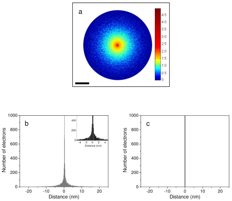
(a) Image of an electron probe at the bottom surface of a 1 μm-thick model specimen calculated with Monte Carlo simulation. The color bar represents number of electrons displayed in base-10 log scale. The broad beam is shown up to a diameter of 50 nm. (b) Line profile across the probe image in (a). The line profile is displayed on linear scale. The central peak at 0 nm extends to almost 100,000 electrons (from 1 million electron trajectories simulated), and the tails in the probe are a manifestation of beam spreading due to multiple elastic scattering in the specimen. Inset shows probe tails in closer detail. (c) Schematic representation of an electron probe focused at the top surface of the model specimen. Specimen features will be imaged with better resolution at the top surface, i.e. in absence of beam spreading. Scale bar = 10 nm.
Fig. 5a now shows the net average angles θn with which electrons arrive at the bottom surface of the 1 μm-thick specimen described above. In Fig. 5a, the average scattering angles (in mrad) of the electrons in the broadened beam were determined within rings of 0.5 nm. A histogram showing the distribution of θn within the probe at the bottom of the thick section is given in Fig. 5b. For comparison, Fig. 5c shows a histogram of θn within the probe for a 200-nm thick specimen. Figs. 5b and 5c illustrate the effect of multiple elastic scattering in spreading the angular distribution of the electrons arriving at the bottom of a thick specimen. Furthermore, as evident from Fig. 5a, electrons which undergo multiple elastic scattering in thick sections are displaced significantly from the center of the probe at the bottom surface.
Fig. 5.
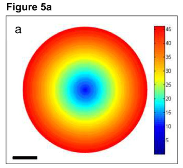


(a) Image displaying average angles with which electrons arrive at the bottom surface of the 1 μm-thick specimen associated with Fig. 4. Color bar is in units of mrad. Average scattering angles within the broad beam are shown up to a beam diameter of 50 nm. Electrons farther from the center of the probe arrive at the bottom of a thick specimen with larger net average scattering angles. (b) Histogram showing the distribution of net scattering angles, θn, at the bottom of the thick model specimen. Electrons with average θn larger than around 50 mrad in (b) do not appear in (a), and thus these fall outside of the 50 nm probe diameter range. (c) For comparison, histogram showing the distribution of net scattering angles θn at the bottom of a 200-nm thick specimen. Scale bar = 10 nm.
Based on Figs. 4 and 5, we can divide a broadened electron probe at the bottom surface of a thick section into three distinct regions. For this, we consider the probe to scan across a cluster of Os atoms located at the bottom surface to form an ADF STEM image of the cluster. Furthermore, we assume here an ADF detector with inner and outer collection semi-angles of βinner and βouter, respectively. Assuming for simplicity that the incident beam convergence angle is 0 mrad, then electrons at the bottom of the specimen and at the exact center of the broad probe would have on average a net scattering angle θn around 0 mrad. These electrons would impinge on the Os cluster at the bottom and be scattered onto the ADF detector with a certain probability P1. The value of P1 would depend both on the number of Os atoms per unit area in the cluster and on the elastic scattering cross section of Os for a specific incident beam energy. Electrons farther from the center of the probe and arriving at the bottom with a net scattering angle 0< θn <βinner (Fig. 5a) would hit the cluster of Os atoms and be scattered onto the ADF detector with probability P2 > P1. Finally, electrons with greater displacement from the center of the probe would have θn such that βinner ≤ θn ≤ βouter. These electrons would impinge on the ADF detector independently of whether the probe scans the Os cluster or the background, and thus their probability P3 of being scattered onto the ADF detector would be approximately 1. These electrons with P3 around 1 would degrade contrast but not resolution of the Os cluster at the bottom of the thick section. Resolution of the cluster would be mostly degraded by those electrons displaced from the center of the probe and with 0< θn <βinner.
The above considerations can be put on a quantitative basis enabling us to assess the effect of different STEM detector configurations on image resolution of thick sections. In the following analysis, we consider the case of ADF STEM imaging, but the case of BF imaging is analogous. The process of image formation for a cluster of Os atoms located at the bottom of a thick biological specimen can be represented as
| (4) |
Where, Na (x,y) is the number of Os atoms per unit area at pixel (x,y); I(x,y)β is the recorded image intensity at pixel (x,y) by an ADF detector subtending a collection semi-angle β; σβ is the integrated elastic scattering cross section of Os atoms for an ADF detector with collection semi-angle β; ⊗ is a convolution symbol. P(x,y) represents the electron probe at the bottom of the section, and is defined as
| (5) |
with the summation in m being performed over all electrons (e) at each (x,y) coordinate in the probe.
In Eq. 4 it is assumed that all electrons arrive at the bottom surface of the specimen and impinge on the Os cluster with a net scattering angle θn of 0 mrad. In reality, Eq. 4 must be modified to incorporate the different angles θn in the broad beam at the bottom of the specimen:
| (6) |
Eq. 6 is identical to Eq. 4 except that now the simple beam broadening function has become , which depends on the net scattering angle θn with which each electron arrives at the bottom of the thick specimen as well as on the collection angle subtended by the ADF detector. Eq. 6 is valid for 0< θn < βinner, since, as mentioned above, electrons with βinner ≤ θn ≤ βouter do not contribute to form an image of the Os cluster. For 0 < θn < βinner, . The ratio is then a factor that accounts for the higher efficiency with which electrons with 0 < θn < βinner are collected by an ADF detector after being scattered by a cluster of Os atoms.
We determined the beam broadening function P(x,y)′ for ADF detectors subtending collection semi-angles of 16-80 mrad and 40-200 mrad, a well as for a BF detector with outer semi-angle of 13 mrad. The calculations were performed for three different specimen thicknesses of 200, 500 and 1000 nm with an assumed composition of 2 atomic percent Os in C. For each specimen thickness, we then determined the fraction of electrons in the broadened beam P(x,y)′ as a function of its diameter (Fig. 6). The results show that for a specimen of 200 nm in thickness, beam spreading is negligible and independent of detector configuration (Fig. 6a) as expected. On the other hand, for a specimen thickness of 1000 nm, beam spreading is significant and highly dependent on detector configuration (Fig. 6c). Specifically, Fig. 6c shows that either an ADF detector with a small inner semi-angle (solid line) or a BF detector with a small outer semi-angle (dashed line) would give rise to STEM images of considerably higher resolution than would be obtained with an ADF detector of large inner semi-angle (dotted line). For a specimen of intermediate thickness (500 nm), Fig. 6b suggests that an ADF detector of large collection angle might not be advantageous for imaging specimen features located at the bottom of a thick specimen.
Fig. 6.

Fraction of electrons within modified beam-broadening function P(x,y)′ as a function of beam diameter. Calculations were done for a specimen of 2 atomic percent Os in C with thickness of (a) 200 nm, (b) 500 nm and (c) 1000 nm. Solid line: ADF STEM detector of 16 mrad inner semi-angle. Dotted line: ADF STEM detector of 40 mrad inner semi-angle. Dashed line: BF STEM detector of 13 mrad outer semi-angle. Curves suggest that ADF detector of large inner angle will give rise to images of poor resolution for specimen features located near the bottom surface of sections around 1 μm thick.
We recorded BF and high-angle ADF STEM images of 20 nm-diameter gold particles situated at the top and bottom surfaces of an approximately 2 μm-thick plastic section. The BF and ADF STEM images were collected simultaneously and thus under identical electron optical conditions. Figs. 7a and 7b show BF and ADF STEM images of gold particles located at the top surface, respectively, whereas Figs. 7c and 7d display BF and ADF STEM images of gold particles located at the bottom surface. The particles located at the top surface exhibit equally good spatial resolution regardless of the detection type. However, in the image focused at the bottom surface the particles appear significantly blurred when a large-angle ADF detector is used, in agreement with Fig. 6c.
Fig. 7.
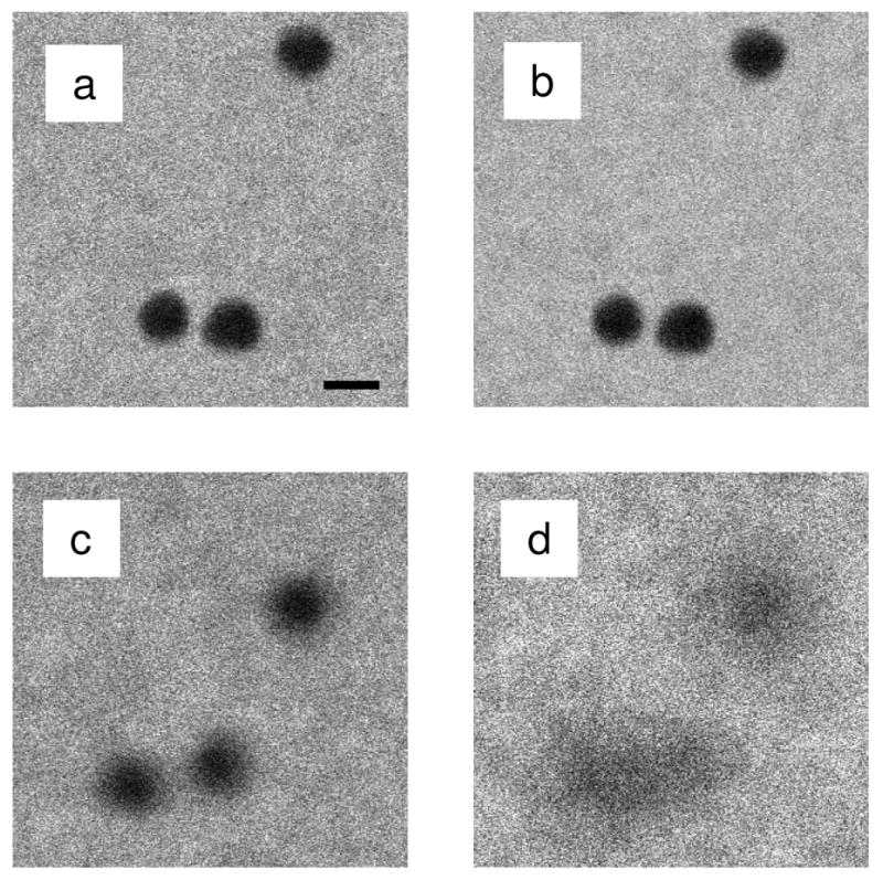
BF and ADF STEM images of 20 nm-diameter gold particles situated at the top and bottom surfaces of a 2 μm-thick plastic section. The BF and ADF images were recorded simultaneously with STEM detectors of 13 mrad outer semi-angle and 40 mrad inner semi-angle, respectively. ADF STEM images are displayed with reversed contrast. (a) BF and (b) ADF STEM images of gold particles located at the top of the section. In the absence of beam spreading, the gold particles appear relatively sharp in both imaging modes. (c) BF and (d) ADF STEM images of gold particles located at the bottom of the section. Beam spreading blurs the particles significantly more in high-angle ADF STEM. Scale bar is 20 nm.
BF and ADF STEM tomography of stained plastic sections of intermediate thickness
The Monte Carlo simulations discussed above suggest that STEM tomographic tilt series of thick (> 1μm) biological specimens stained with heavy elements are best acquired using a BF detector of small outer collection semi-angle. With such a detector, contrast and SNR would be comparable to that obtained with an ADF detector of large collection angle (Fig. 3), but a higher spatial resolution should be achievable for reconstructing objects situated at the bottom surface of the thick section (Fig. 6). It should be pointed out that whereas crystalline material science specimens require the use of BF detectors of large outer semi-angle to achieve incoherent imaging [22], for most biological specimens incoherent imaging conditions can be obtained with a BF detector of small outer semi-angle (e.g., 15 mrad) due to the amorphous nature of these specimens.
The choice of optimal STEM detector geometry for STEM tomography of sections of intermediate thickness (around 500 nm) is less straightforward, but the results again suggest that a BF detector might be preferable to an ADF detector. Use of an ADF detector of small inner semi-angle (e.g. 15 mrad) would be unsuitable for STEM tomography of sections around 500 nm in thickness because contrast and SNR would degrade abruptly with increasing tilt angle. On the other hand, an ADF detector of large inner semi-angle would produce images of good contrast and SNR for all tilt angles, although for higher tilt angles the resolution would be poor for objects situated near the bottom surface of the specimen.
We collected BF and ADF STEM tilt series from a 600 nm-thick plastic-embedded and stained section of C. elegans to test our prediction that a BF detector would be advantageous for imaging specimens of only moderate thickness. The BF and ADF tilt series were collected simultaneously and therefore under identical conditions. The BF tilt images were acquired with a detector outer semi-angle of 13 mrad, and the ADF images were recorded with a detector inner semi-angle of 40 mrad.
Slices across the BF and ADF STEM tomographic reconstructions obtained from the top region of the specimen are shown in Figs. 8a and 8b, respectively. It is seen that BF and high-angle ADF STEM tomography yield reconstructions of comparable quality for regions of a semi-thick specimen that are close to the top surface. In Figs. 8a and 8b, double-track features typical of unit bilayer membranes are clearly visible in some vesicles, indicating a resolution of better than 5 nm. Figs. 8c and 8d show slices across the BF and ADF STEM tomographic reconstructions obtained from regions near the bottom surface. As expected, the BF STEM reconstruction shows higher resolution than the ADF STEM reconstruction.
Fig. 8.
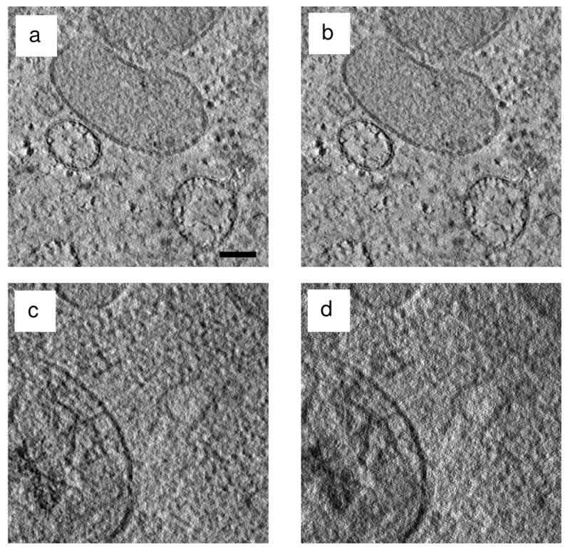
7-nm thick tomographic slices from reconstructed BF and ADF STEM tilt series of a 600 nm-thick stained plastic-embedded section of C. elegans. The tilt series were recorded simultaneously using BF and ADF STEM detectors of 13 mrad outer semi-angle and 40 mrad inner semi-angle, respectively. Slices from ADF STEM reconstructions are displayed with reversed contrast. (a)-(b) Slices across the top region of (a) BF and (b) ADF STEM reconstructed tomograms. The slices appear virtually indistinguishable from each other, indicating that either technique would be suitable for 3D reconstruction of the top region of moderately thick stained biological specimens. (c)-(d) Slices across the bottom region of reconstructed (c) BF and (d) ADF STEM tomograms. BF STEM tomography yields 3D reconstructions with significantly better resolution for specimen features located at the bottom of moderately thick specimens. Scale bar is 100 nm.
Finally, we point out that the dependence of image resolution on STEM detector geometry should be significantly more noticeable in an electron tomogram than in a 2D projection image. In particular, this situation arises for specimens of moderate thickness (up to around 1 μm) and when specimen features run more or less parallel to the z axis of the section. In this case, a 2D projection image is formed by combining high-resolution information from the top region of the specimen with low resolution information from the bottom region, and thus the overall resolution of the image is only partially affected by the blurred contribution from the bottom part of the specimen. For thicker sections, the top region which preserves high resolution information contributes only to a fraction of the total projected signal, and thus the dependence of image resolution on detector geometry should be more noticeable. For instance, Hallégot and Zaluzec [38] have provided some examples of 2D projection images of very thick biological sections (around 5 μm and higher) imaged with a scanning confocal electron microscope [39]. By allowing for the removal of spurious electrons that have been multiply scattered, the authors achieved a significant improvement in the resolution of the 2D projection images when compared with other traditional imaging modes. For 3D imaging with electron tomography, we have shown above that the resolution in the region near the bottom surface of a stained biological section depends significantly on the specific configuration of the STEM detection system, even for sections of moderate thickness (e.g. 600 nm), which is in agreement with the trends derived from the Monte Carlo simulation.
Conclusions
We have implemented a Monte Carlo electron-trajectory simulation program to investigate optimum STEM tomography imaging strategies for stained biological specimens. Our Monte Carlo simulations suggest that STEM tomography tilt series of thick stained sections is optimally performed with a BF detector. For thick sections, the simulations showed that a BF detector gives rise to images of good contrast and SNR comparable to that obtained with an ADF detector of large inner angle, while also minimizing image blurring caused by beam broadening. We also experimentally investigated the quality of BF and high-angle ADF STEM tomographic reconstructions obtained from a 600 nm-thick stained section of C. elegans. The quality of reconstruction at the top region of the specimen was similar for the BF and ADF STEM detectors. However, at the bottom region of the specimen, the BF STEM detector yielded a tomographic reconstruction with better resolution. Imaging thick, stained biological specimens in 3D with a spatial resolution that reveals membranes and macromolecular assemblies can be an attractive way to study structures of whole cellular organelles, bacteria and small eukaryotic microorganisms. To that end, BF STEM tomography could be a useful alternative to other TEM-based techniques.
Acknowledgments
This work was supported by the Intramural Research Program of the National Institute of Biomedical Imaging and Bioengineering, National Institutes of Health. MFHM would like to acknowledge support of a US National Research Council Postdoctoral Associateship co-funded by the National Institute of Standards and Technology and NIBIB, NIH.
Footnotes
Publisher's Disclaimer: This is a PDF file of an unedited manuscript that has been accepted for publication. As a service to our customers we are providing this early version of the manuscript. The manuscript will undergo copyediting, typesetting, and review of the resulting proof before it is published in its final citable form. Please note that during the production process errors may be discovered which could affect the content, and all legal disclaimers that apply to the journal pertain.
References
- 1.Koster AJ, Grimm R, Typke D, Hegerl R, Stoschek A, Walz J, Baumeister W. J Struct Biol. 1997;120:276. doi: 10.1006/jsbi.1997.3933. [DOI] [PubMed] [Google Scholar]
- 2.McEwen BF, Marko M. J Histochem Cytochem. 2001;49:553. doi: 10.1177/002215540104900502. [DOI] [PubMed] [Google Scholar]
- 3.McIntosh R, Nicastro D, Mastronarde D. Trends Cell Biol. 2005;15:43. doi: 10.1016/j.tcb.2004.11.009. [DOI] [PubMed] [Google Scholar]
- 4.He W, Cowin P, Stokes DL. Science. 2003;302:109. doi: 10.1126/science.1086957. [DOI] [PubMed] [Google Scholar]
- 5.Radermacher M. Weighted back-projection methods. In: Frank J, editor. Electron Tomography Methods for Three-Dimensional Visualization of Structures in the Cell. second. Plenum Press; New York: 2006. [Google Scholar]
- 6.Bouwer JC, Mackey MR, Lawrence A, Deerinck TJ, Jones YZ, Terada M, Martone ME, Peltier S, Ellisman MH. J Struct Biol. 2004;148:297. doi: 10.1016/j.jsb.2004.08.005. [DOI] [PubMed] [Google Scholar]
- 7.Soto GE, Young SJ, Martone ME, Deerinck TJ, Lamont S, Carragher BO, Hama K, Ellisman MH. Neuroimage. 1994;1:230. doi: 10.1006/nimg.1994.1008. [DOI] [PubMed] [Google Scholar]
- 8.Ladinsky MS, Mastronarde DN, McIntosh JR, Howell KE, Staehelin LA. J Cell Biol. 1999;144:1135. doi: 10.1083/jcb.144.6.1135. [DOI] [PMC free article] [PubMed] [Google Scholar]
- 9.Noske AB, Costin AJ, Morgan GP, Marsh BJ. J Struct Biol. 2007;161:298. doi: 10.1016/j.jsb.2007.09.015. [DOI] [PMC free article] [PubMed] [Google Scholar]
- 10.Henderson GP, Gan L, Jensen GJ. PLoS One. 2007;2(8):e749. doi: 10.1371/journal.pone.0000749. [DOI] [PMC free article] [PubMed] [Google Scholar]
- 11.Reimer L, Rennekamp R, Fromm I, Langenfeld M. J Microsc. 1991;162:3. doi: 10.1111/j.1365-2818.1991.tb03111.x. [DOI] [PubMed] [Google Scholar]
- 12.Körtje KH, Paulus U, Ibsch M, Rahmann H. J Microsc. 1996;183:89. [PubMed] [Google Scholar]
- 13.Han KF, Sedat JW, Agard DA. J Microsc. 1995;178:107. doi: 10.1111/j.1365-2818.1995.tb03586.x. [DOI] [PubMed] [Google Scholar]
- 14.Han KF, Sedat JW, Agard DA. J Struct Biol. 1997;120:237. doi: 10.1006/jsbi.1997.3914. [DOI] [PubMed] [Google Scholar]
- 15.Colliex C, Mory C, Olins AL, Olins DE, Tencé M. J Microsc. 1989;153:1. doi: 10.1111/j.1365-2818.1989.tb01462.x. [DOI] [PubMed] [Google Scholar]
- 16.Beorchia A, Heliot L, Menager M, Kaplan H, Ploton D. J Microsc. 1993;170:247. doi: 10.1111/j.1365-2818.1993.tb03348.x. [DOI] [PubMed] [Google Scholar]
- 17.Yakushevska AE, Lebbink MN, Geerts WJ, Spek L, van Donselaar EG, Jansen KA, Humbel BM, Post JA, Koster AJ. J Struct Biol. 2007;159:381. doi: 10.1016/j.jsb.2007.04.006. [DOI] [PubMed] [Google Scholar]
- 18.Ziese U, Kübel C, Verkleij AJ, Koster AJ. J Struct Biol. 2002;138:58. doi: 10.1016/s1047-8477(02)00018-7. [DOI] [PubMed] [Google Scholar]
- 19.Cheutin T, O'Donohue MF, Beorchia A, Klein C, Kaplan R, Ploton D. J Histochem Cytochem. 2003;51:1411. doi: 10.1177/002215540305101102. [DOI] [PMC free article] [PubMed] [Google Scholar]
- 20.Sousa AA, Aronova MA, Kim YC, Dorward L, Zhang G, Leapman RD. J Struct Biol. 2007;159:507. doi: 10.1016/S1047-8477(08)00063-4. [DOI] [PubMed] [Google Scholar]
- 21.Hyun JK, Ercius P, Muller DA. Ultramicroscopy. 2008 doi: 10.1016/j.ultramic.2008.07.003. doi:10.1016/j.ultramic.2008.07.003. [DOI] [PubMed] [Google Scholar]
- 22.Ercius PA, Weyland M, Muller DA, Gignac LM. Appl Phys Lett. 2006;88:243116. [Google Scholar]
- 23.Levine ZH. Appl Phys Lett. 2003;82:3943. [Google Scholar]
- 24.Levine ZH. J Appl Phys. 2005;97:033101. [Google Scholar]
- 25.Joy DC. Monte Carlo Modeling for Electron Microscopy and Microanalysis. Oxford University Press; New York: 1995. [Google Scholar]
- 26.Hovington P, Drouin D, Gauvin R. Scanning. 1997;19:1. doi: 10.1002/sca.4950210403. [DOI] [PubMed] [Google Scholar]
- 27.Reichelt R, Engel A. Ultramicroscopy. 1984;13:279. [Google Scholar]
- 28.Newbury DE, Myklebust RL. Ultramicroscopy. 1979;3:391. [Google Scholar]
- 29.Reichelt R, Carlemalm W, Villiger W, Engel A. Ultramicroscopy. 1985;16:69. [Google Scholar]
- 30.Reichelt R, Engel A. Ultramicroscopy. 1986;19:43. doi: 10.1016/0304-3991(86)90006-9. [DOI] [PubMed] [Google Scholar]
- 31.Gauvin R, L'Espérance G. J Microsc. 1992;168:153. [Google Scholar]
- 32.Jablonski A, Salvat F, Powell CJ. Electron Elastic-scattering Cross-section Database (Version 3.1) SRD 64. National Institute of Standards and Technology; Gaithersburg: 1993. [Google Scholar]
- 33.Kremer JR, Mastronarde DN, McIntosh JR. J Struct Biol. 1996;116:71. doi: 10.1006/jsbi.1996.0013. [DOI] [PubMed] [Google Scholar]
- 34.Rose H, Fertig J. Ultramicroscopy. 1976;2:77. doi: 10.1016/s0304-3991(76)90518-0. [DOI] [PubMed] [Google Scholar]
- 35.Smith DJ, Cowley JM. Ultramicroscopy. 1975;1:127. doi: 10.1016/s0304-3991(75)80015-5. [DOI] [PubMed] [Google Scholar]
- 36.Groves T. Ultramicroscopy. 1975;1:15. doi: 10.1016/s0304-3991(75)80005-2. [DOI] [PubMed] [Google Scholar]
- 37.Gentsch P, Gilde H, Reimer L. J Microsc. 1974;100:81. [Google Scholar]
- 38.Hallégot P, Zaluzec NJ. Microsc Microanal. 2004;10(Suppl 2):1290. [Google Scholar]
- 39.Zaluzec NJ. Microsc Today. 2003;5:8. [Google Scholar]