Abstract
Electric field-controlled ferromagnetism of (Zn,Co)O is demonstrated via anomalous Hall effect measurements. The electron carrier concentration in this material is 1.65×1020 cm−3 as measured via ordinary Hall effect at 4 K, and an anomalous Hall effect is observed up to 6 K, but with no hysteresis at any temperature. With positive electric gate field, the carrier concentration is increased by approximately 2%, resulting in a clear magnetic hysteresis at 4 K. The ability to reversibly induce∕eliminate ferromagnetism by applied gate field alone, measured via the effect on the carriers, is a clear sign of carrier-induced ferromagnetism in this system.
There is currently great interest in understanding and manipulating the physical properties of magnetic semiconductors (MSs) due to their potential use in spintronic devices where both the electronic charge and spin degrees of freedom can be exploited.1 Although many kinds of MSs exhibiting high-temperature ferromagnetism have been identified,2, 3 the microscopic origin of the magnetic properties is still quite controversial in general for all the II-VI, and especially ZnO,4, 5, 6 based materials. ZnO doped with Co is a promising II-VI magnetic semiconductor. It has been theoretically predicted that (Zn,Co)O can be ferromagnetic above room temperature. In the literature, various magnetically doped oxide semiconductors have been claimed to exhibit ferromagnetism at or even well above room temperature.7, 8 However, the possibility of an extrinsic origin for the ferromagnetism from segregation of magnetic dopants or impurities cannot be ruled out in many of these cases.9, 10, 11 The most common methods used to characterize magnetic semiconductor films, including crystallography and magnetometry, are unable to distinguish intrinsic carrier mediated ferromagnetism from extrinsic, spurious sources of magnetism.12, 13 For a true ferromagnetic semiconductor, magnetism needs to be caused by an exchange interaction between magnetic ion and spin polarized carriers, which can be directly probed using magneto transport or anomalous Hall effect (AHE). Ideally, the question as to how the carrier density affects the magnetic character should be answered by varying the carrier density without changing the host structure as was done for (In,Mn)As.14 Here, we demonstrate electric field control of ferromagnetism of (Zn,Co)O thin films in a gated field effect transistor (FET) structure where we are able to reversibly vary the magnetization of electron-induced ferromagnetism by applying an electric field.
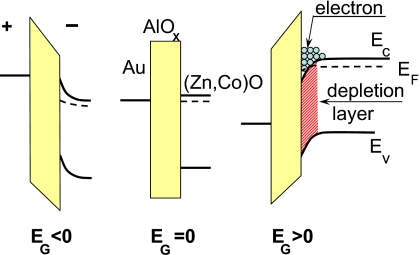
We have fabricated a metal-insulator-semiconductor FET structure as shown in Fig. 1 to look for carrier-induced ferromagnetism. An increase or decrease of electron concentration (ZnO is naturally n-type due to Zn interstitials, which easily form due to the large ionicity of ZnO)15 by application of electric field is expected to result in an increase∕decrease of electron-mediated ferromagnetic exchange between localized Co spins. Using this technique, we are able to tune the carrier concentration while keeping the magnetic dopant concentration, structure, and local arrangement constant. We have fabricated this structure and used it to study magnetism via measurement of the AHE as a function of gate field (i.e., electron concentration) and temperature. We use this to conclusively demonstrate carrier-induced ferromagnetism at low temperature in Co-doped ZnO.
Figure 1.
Schematic energy band diagram for reverse (EG<0), neutral (EG=0), and forward (EG>0) biased (Zn,Al,Co)O-based FET device. Positive gate electric field increases electron concentration in the depletion layer (Zn,Co)O resulting in enhancement of the ferromagnetic interaction between Co ions, whereas negative gate voltage decreases the concentration and reduces the interaction.
To fabricate the FET, 23-nm-thick (Zn0.88Co0.1Al0.02)O was grown at 550 °C on an amorphous 500 nm SiOx layer grown on a Si (100) substrate by rf-magnetron sputtering (base pressure ∼1×10⁻⁸ Torr). Al is a well known n-type dopant in ZnO systems and was codoped in the (Zn,Co)O system in order to provide sufficient carriers to produce conductivity at low temperature. The sample was processed by photolithography and wet etched into a Hall bar geometry [40 μm width, 140 μm length, with current (I), transverse (Vxy), and longitudinal (Vxx) contacts]. An 80-nm-thick insulating AlOx layer was deposited on this sample using rf-reactive sputtering at room temperature using an oxygen∕Ar mixed gas. Finally, a 5 nm Cr∕50 nm Au top gate electrode was defined by a lift-off process, and contact was made to the source, drain, and bridge terminals by indium bonding. The gate leakage current (measured at 4 K) is found to be less than 10 nA in all devices and the breakdown gate field is determined to be consistently greater than 8 MV∕cm (∼70 V). With this FET, the gate electric field is used to modulate the electron density of the two-dimensional (2D) subbands in the ZnO layer as shown in Fig. 1. The samples’ characteristics and results obtained from ten FET samples fabricated thus far show similar reproducible results.
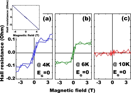
In contrast to the large AHE signal found in III-V MSs such as (Ga,Mn)As or (In,Mn)As, the oxide-based MSs exhibit a weak AHE signal compared to the ordinary Hall effect (OHE).16 In order to detect the presence of the anomalous Hall signal, we employed a method of ac phase sensitive detection using a lock-in amplifier at 16 Hz. Currents were kept at or below 1 μA in order to avoid heating the sample. Hall resistance Rxy (=Vxy∕I) data as a function of applied magnetic field H at a gate field EG=0 are shown in Fig. 2 at various temperatures T. The nonlinear “s”-shape of Rxy(H) indicates the presence of both the OHE and AHE in our (Zn,Co)O samples. The nonlinearity and magnitude of Rxy(H) decrease with increasing temperature with no magnetic field dependence above 10 K. The data were analyzed by first finding the odd and even components of Rxy(H) The even component is due to small (inevitable) offsets in Vxy contacts, which lead to magnetoresistance contributions [proportional to Rxx(H)]. The odd component is due to the Hall effect, both ordinary and anomalous. To obtain the AHE contribution, we fit Rxy(H) for ∣H∣>3 T to a straight line and subtracted this linear OHE contribution from the total. The insets show the odd component of the Rxy(H) data before subtraction of the OHE. The negative slope indicates electrons as carriers as expected from Al doping and native electron background due to Zn interstials.16 This carrier concentration depends weakly on temperature. The electron concentration determined by the OHE of (ZnCoAl)O at 4 K is about 1.65×1020 cm−3 (3.813×1014 cm−2 for these thin samples). OHE measurements on samples prepared without Co show a lower electron concentration (approximately a factor of 2) than those with Co, likely due to Co interstitials, and no AHE was observed at low temperature in ZnO:Al sputtered by the same method without Co.
Figure 2.
Magnetic field dependence of Hall resistance at 4, 6, and 10 K with zero applied gate electric field. Inset shows raw data (odd component) of transverse resistance Rxy vs applied magnetic field H. AHE data in main figures are obtained by taking the odd part of Rxy(H){[Rxy(H)−Rxy(−H)]∕2} with linear fit (∣H∣>3 T) subtracted.
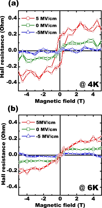
By applying different gate electric fields, the electron concentration is reversibly tuned causing a small change in the linear part of Rxy(H) and a significant change in the nonlinear AHE. A 5 MV∕cm gate electric field, in a model of a 2D electron gas, is expected to produce an electron concentration change. The change of 5.4×1012 cm−2 was experimentally verified by analysis of the linear Rxy(H) (OHE), causing the electron concentration of the samples to change by approximately 2% at 4 K. Figure 3 shows the Hall resistance as a function of magnetic field at 4 and 6 K under three different gate electric fields. For positive gate electric field, the AHE is dramatically changed and a hysteresis loop is clearly visible at 4 K. By comparison, changing the gate electric field to −5 MV∕cm causes the linear ordinary Hall resistance to slightly increase (as expected for lower carrier concentration) and no hysteresis is observed at any temperature. Figure 3 shows a general trend of decreasing AHE with increasing temperature down to 4 K for all gate electric field as expected since the AHE is dependent on the sample’s magnetization which decreases with increasing temperature.
Figure 3.
Magnetic field dependence of Hall resistance Rxy for various electric gate field and temperature. (a) By applying positive gate field, electrons are accumulated in the (Zn,Co)O layer and a clear hysteresis at 4 K appears, which is not present for zero and negative gate field. (b) At 6 K, no hysteresis is observed in the Hall resistance measurement at any gate field. The Hall resistance gradually increases with increasing gate electric field at both temperatures.
There are many reports of the AHE in ZnO based magnetic semiconductors but this is the first measurement of gate-controlled carrier density modulated magnetism in this magnetic semiconductor. As with other researchers, we are not able to rule out formation of unexpected phases during the growth process, however the gate modulation of the AHE in (Zn,Co)O clearly shows enhancement of the magnetic properties with increasing carrier concentration. In particular, we observe that a positive gate field increases the electron population in the layer (Zn,Co)O thin film as seen by a decrease in OHE. This small increase in carrier concentration drives the sample into a ferromagnetic state at higher Tc as observed by the ferromagnetic hysteresis in the Hall measurement at 4 K at EG=5 MV∕cm, and not at 0 or −5 MV∕cm. The ability to induce ferromagnetism in these Co-doped ZnO films by applied gate electric field shows that ferromagnetism originates from an electron-mediated exchange interaction. Thus by independently changing the magnetic moment to charge carrier ratio, one can tune the magnetic properties of these magnetic semiconductors. At higher temperatures, the OHE dominates because of the decreasing susceptibility (standard Curie–Weiss behavior) of the (Zn,Co)O current driven layer with increasing temperature and AHE (including s-like shape) disappears above 10 K.
Gate-tuned control of the magnetic properties has previously been observed in the III–V magnetic semiconductor, (In,Mn)As, for hole (∼1.6×1020 cm−3)-mediated ferromagnetism with a maximum Tc of around 27 K.14 Here we report the first electric field-controlled ferromagnetism in (Zn,Co)O thin films in a gated field effect transistor structure. In this magnetic oxide we have observed, for an electron concentration about 1.65×1020 cm−3, electron-mediated ferromagnetism below 10 K. We expect an increased Curie temperature with increasing Co concentration and initial carrier concentration, which can be controlled during the thin film deposition process, for instance, by changing the oxygen partial pressure or growth temperature and by changing the Al dopant concentration.
Acknowledgments
We would like to thank Danial Queen and Micol Alemani for discussions and help. Materials synthesis and characterization were supported by DOE Division of Materials Sciences and Engineering under Contract No. DE-AC02-05CH11231 and device fabrication and analysis were supported by Western Institute of Nanoelectronics.
References
- Ohno H., Science 281, 951 (1998). 10.1126/science.281.5379.951 [DOI] [PubMed] [Google Scholar]
- Kittilstved K. R., Schwartz D. A., Tuan A. C., Heald S. M., Chambers S. A., and Gamelin D. R., Phys. Rev. Lett. 97, 037203 (2006). 10.1103/PhysRevLett.97.037203 [DOI] [PubMed] [Google Scholar]
- He Y., Sharma P., Biswas K., Liu E. Z., Ohtsu N., Inoue A., Inada Y., Nomura M., Tse J. S., Yin S., and Jiang J. Z., Phys. Rev. B 78, 155202 (2008). 10.1103/PhysRevB.78.155202 [DOI] [Google Scholar]
- Snure M., Kumar D., and Tiwari A., Appl. Phys. Lett. 94, 012510 (2009). 10.1063/1.3067998 [DOI] [Google Scholar]
- Mandal S. K., Das A. K., Nath T. K., Karmakar D., and Satpati B., J. Appl. Phys. 100, 104315 (2006). 10.1063/1.2360387 [DOI] [Google Scholar]
- Sato K. and Katayama-Yoshida H., Semicond. Sci. Technol. 17, 367 (2002). 10.1088/0268-1242/17/4/309 [DOI] [Google Scholar]
- Liu Y. and MacManus-Driscoll J. L., Appl. Phys. Lett. 94, 022503 (2009). 10.1063/1.3068753 [DOI] [Google Scholar]
- Song C., Geng K. W., Zeng F., Wang X. B., Shen Y. X., Pan F., Xie Y. N., Liu T., Zhou H. T., and Fan Z., Phys. Rev. B 73, 024405 (2006). 10.1103/PhysRevB.73.024405 [DOI] [Google Scholar]
- Liu Q., Gan C. L., Yuan C. L., and Han G. C., Appl. Phys. Lett. 92, 032501 (2008). 10.1063/1.2835702 [DOI] [Google Scholar]
- Barla A., Schmerber G., Beaurepaire E., Dinia A., Bieber H., Colis S., Scheurer F., Kappler J. -P., Imperia P., Nolting F., Wilhelm F., Rogalev A., Müller D., and Grob J. J., Phys. Rev. B 76, 125201 (2007). 10.1103/PhysRevB.76.125201 [DOI] [Google Scholar]
- Rode K., Mattana R., Anane A., Cros V., Jacquet E., Contour J. -P., Petroff F., Fert A., Arrio M. -A., Sainctavit Ph., Bencok P., Wilhelm F., Brookes N. B., and Rogalev A., Appl. Phys. Lett. 92, 012509 (2008). 10.1063/1.2829610 [DOI] [Google Scholar]
- Ando K., Science 312, 1883 (2006). 10.1126/science.1125461 [DOI] [PubMed] [Google Scholar]
- Toyosaki H., Yamada Y., Nakajima K., Chikyow T., Hasegawa T., Koinuma H., Kawasaki M., and Fukumura T., Nature Mater. 3, 221 (2004). 10.1038/nmat1099 [DOI] [PubMed] [Google Scholar]
- Ohno H., Chiba D., Matsukura F., Omiya T., Abe E., Dietl T., Ohno Y., and Ohtani K., Nature (London) 408, 944 (2000). 10.1038/35050040 [DOI] [PubMed] [Google Scholar]
- Zhang S. B., Wei S. H., and Zunger A., Phys. Rev. B 63, 075205 (2001). 10.1103/PhysRevB.63.075205 [DOI] [Google Scholar]
- Xu Q., Hartmann L., Schmidt H., Hochmuth H., Lorenz M., Schmidt-Grund R., Sturm C., Spemann D., and Grundmann M., Phys. Rev. B 73, 205342 (2006). 10.1103/PhysRevB.73.205342 [DOI] [Google Scholar]


