Abstract
We have investigated the effects of piezoelectric potential in a ZnO nanowire on the transport characteristics of the nanowire based field effect transistor through numerical calculations and experimental observations. Under different straining conditions including stretching, compressing, twisting, and their combination, a piezoelectric potential is created throughout the nanowire to modulate∕alternate the transport property of the metal-ZnO nanowire contacts, resulting in a switch between symmetric and asymmetric contacts at the two ends, or even turning an Ohmic contact type into a diode. The commonly observed natural rectifying behavior of the as-fabricated ZnO nanowire can be attributed to the strain that was unpurposely created in the nanowire during device fabrication and material handling. This work provides further evidence on piezopotential governed electronic transport and devices, e.g., piezotronics.
INTRODUCTION
Zinc oxide (ZnO) is an important semiconductive and piezoelectric material for electronics, optoelectronics, sensors, and energy science.1, 2 ZnO-based nanostructures are diverse and abundant with a great potential for nanotechnology.3 Recently, various novel devices have been fabricated using ZnO nanowires∕nanobelts, such as piezoelectric power generators,4 field-effect transistor (FET),5 ultraviolet photodetectors,6 Schottky diodes and switches,7 and flexible piezotronic strain sensors.8 A key issue for all of these devices is that their performances are largely dictated by the contacts between the ZnO nanowire and the metal electrodes. Distinctly different current-voltage (I-V) characteristics have been observed for devices fabricated using identical electrode materials and nanowires of similar size and doping concentration, and prepared under same conditions. They can be grouped into three types: a rectifying feature, which is a result of asymmetric contacts at the two ends of the nanowire, a linear I-V dependence, which implies that both of the two contacts are Ohmic type, and a symmetrically downward bending I-V demeanor, which corresponds to the symmetric Schottky contacts. We now use a practical example to illustrate the asymmetric contacts formed at the two ends of a ZnO nanowire.
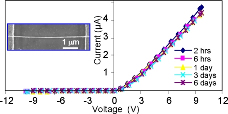
We previously found a spontaneous formation of a Au∕ZnO nanobelt Schottky diode I-V transport property in 80% of the as fabricated nanodevices.9 The rectifying behavior was quite stable, as shown in Fig. 1, the last measurement performed 7 days after the device was exposed to air was consistent with the data obtained 2 h after the device was fabricated.9 The origin of the rectifying behavior is unlikely caused by the different polarity surfaces of the ZnO nanowire provided it is along c-axis because the contacts are at the same side surface of nanowire, either {2-1-10} or {01-10}, lying on the gold electrodes and the cation- or anion-terminated surface has very limited effect on the transport unless the contacts are only at the top and bottom ends of the nanowire.9
Figure 1.
Rectifying transport behavior of a single ZnO nanobelt lying on a pair of Au electrodes. The data were acquired at different times after the fabrication, showing the stability of the device. The inset is a scanning electron microscopy (SEM) image of the device (adopted from Ref. 9).
Even though the Schottky barrier height is difficult to control, since it depends not only on the difference between the work functions of the metal and nanowire but also on the pinning of the Fermi energy by surface states,10 and can be alternated by many other factors, such as image force, field penetration, and the existence of an interfacial insulating layer,11 however, as it happens, the two ends of one nanowire might not have significantly different densities of surface states or of accumulated electrons induced by oxide insulating layer, or any other significant variations of physical characteristics that could drastically affect the contact behaviors at the two ends. Therefore, it is intriguing that one ZnO nanowire device would naturally exhibit significantly different Schottky barrier heights or even have two types of contacts at its two ends. We cannot simply attribute this phenomenon to experimental uncertainty, as it is not a random but a common and stable behavior.
The objective of this paper is to provide an explanation about the phenomena illustrated above. Our main idea is introducing strain created unpurposely in nanowire during device fabrication and material handling, which is rather difficult to control owing to the small size of the nanowires. The naturally built-in strain in the ZnO nanowire creates a piezoelectric potential, which can significantly change the Schottky barrier heights at the two ends. This model is established through numerical calculations and our experimental observations. The results suggest that handling of nanowires is important in dictating their electrical transport properties, especially for piezoelectric nanostructures.
PIEZOELECTRIC POTENTIAL DISTRIBUTION UNDER DIFFERENT STRAINING STATES
Previously we have experimentally demonstrated that when purposely applying a strain on a ZnO nanowire, the generated piezoelectric potential would induce an asymmetric change in Schottky barrier height at the source and drain electrodes of the ZnO wires based FET.7, 8 By piezoelectric potential we mean the potential created by the charges of ions in the crystal that experience a polarization when subjected to straining. The ionic charges are affixed to the atoms and they cannot freely move as long as the strain is preserved. In practice, strain can be introduced without any purpose especially for nanomaterials during device fabrication. During device fabrication, many processes will unavoidably introduce all kinds of strains. For example, if we use silver paste as electrodes, when the silver gets dried, the nanowire is stretched. The nanowire could also be twisted and∕or stretched during manipulation. It inspires us to assume that the transport behavior of a two-end contacted ZnO nanowire device is strongly affected by piezoelectric potential produced by strain.
In our experiments, we used a polymethylmethacrylate (PMMA) film as substrate, on which the two ends bonded nanowire was affixed. The two ends of the nanowire were contacted with the use of silver paste, which bonded the nanowire on the substrate as it dried. By introducing different strains in the polymer substrate by slight bending of its shape, we can introduce various mechanical deformations in the nanowire when the device was built.
The main part of a typical two-terminal nanoelectronic device is a hexagonal ZnO nanowire grown along c-axis with its two ends and short segments adjacent to the ends fully embraced by electrodes, where several kinds of forces, including tensile, compression, twisting and combinations of them, act on the nanowire. Our first task is to calculate the piezoelectric potential distribution throughout the nanowire under these forces. It belongs to a static piezoelectric problem that can be described by four equations: mechanical equilibrium equation [Eq. 1], Gauss’ law of electric field [Eq. 2], fundamental piezoelectric equations [Eq. 3], and compatibility equation [Eq. 4].12, 13 In order to simplify the system and concentrate on observing how the piezoelectric potential would vary with different applied strains, we assume there is no body force and no free charge in the nanowire, hence the divergence of the stress tensor σ is equal to zero for static mechanical equilibrium,
| (1) |
and Gauss equation is satisfied by the electric displacement ,
| (2) |
The constitutive relations between σ and are expressed by fundamental piezoelectric equations,
| (3) |
where is the electric field, cE is the elasticity matrix, e is the piezoelectric coupling matrix, κ is the dielectric matrix, and ε is the strain tensor, which needs to satisfy the compatibility equation,
| (4) |
The acting region of the force introduced during device fabrication should include the entire exterior surface of a segment by the end of nanowire, since in practice, it is almost impossible to make a metal-nanowire contact just at the very end surface of the nanowire. Hence we separate the nanowire into three domains, with the two side domains as the contact regions where the force is applied.
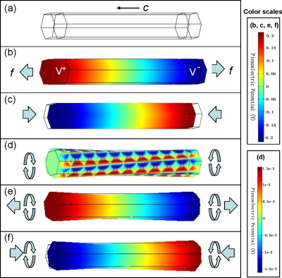
The fully coupled Eqs. 1, 2, 3, 4 can be solved with finite element method. For simplicity of illustrating the proposed physical model, the charge carriers in ZnO have been ignored, which greatly simplify the numerical approach. Figure 2a shows a ZnO nanowire without any applied force. The total length of the nanowire is 1200 nm with a 100 nm length of contact domain at each end, and the side length of the hexagonal is 100 nm. The material constants used in the calculation are anisotropic elastic constants c11=207 GPa, c12=117.7 Gpa, c13=106.1 GPa, c33=209.5 Gpa, c44=44.8 GPa, c55=44.6 GPa, piezoelectric constants e31=−0.51 C∕m2, e33=1.22 C∕m2, e15=−0.45 C∕m2, and relative dielectric constants , .
Figure 2.
Numerical calculation of the piezoelectric potential distribution in a ZnO nanowire without doping. (a) An unstrained ZnO nanowire grown along c-axis with a length of 1200 nm and a hexagonal side length of 100 nm. Two ends of the nanowire are assumed to be surrounded by electrodes for a length of 100 nm. Three-dimensional views of the piezoelectric potential distribution together with deformation shape for the nanowire (b) at a stretching force of 85 nN, (c) at a compressing force of 85 nN, (d) at a twist force pair of 60 nN, (e) at a combination of 85 nN stretching force and 60 nN twist force, and (f) at a combination of 85 nN compressing force and 60 nN twist force. The stretching and compressing forces are supposed to uniformly act on both the end surfaces and side surfaces of the nanowire segments surrounded by electrodes, and the twist force is uniformly applied on the side surfaces of the nanowire segments surrounded by electrodes. The red side is the positive potential side and the blue side is the negative potential side. The potential difference is around 0.4 V. Note the color scale is the same for (b), (c), (e), and (f) but (d) has a much smaller scale.
When a stretching force of 85 nN is uniformly acting on the nanowire surfaces surrounded by electrodes in the direction parallel to c-axis, the length of the nanowire would increase for 0.02 nm, which produces a tensile strain of 2×10⁻⁵. As shown in Fig. 2b, it creates a potential drop of approximately 0.4 V between the two end sides of the nanowire with the +c-axis side of higher potential. When the applied force changes to a compressive, the piezoelectric potential reverses with the potential difference remaining 0.4 V but with the −c-axis side at a higher potential. As presented in Fig. 2c, the nanowire length decreases for 0.02 nm, revealing a compressive strain of −2×10⁻⁵. Note that to produce the same amount of piezoelectric potential, the deformation needed here is much smaller than that in the case of bending a nanowire by a transverse force as we previously demonstrated.14 Thus the force along the polarization direction (c-axis) is easy to produce a high piezoelectric potential. It implies that the experimental setup of applying a force laterally along the c-axis can be a good method to fabricate strain sensor8 and nanogenerator.15
No matter stretching or compressing, the piezoelectric potential continuously drops from one side of the nanowire to the other, which means that the electron energy continuously increases from the one side to the other. Meanwhile, the Fermi level will be flat all over the nanowire when equilibrium is achieved, since there is no external electrical field. As a result, the electron energy barrier between ZnO and metal electrode will be raised at one side and lowered at the other side, which can be observed experimentally as an asymmetric I-V characteristic. This is the governing principle for understanding the experimental results presented in Sec. 3. As the strain is unavoidable during nanowire device fabrication, we would observe rectifying transport behavior for so many as-fabricated nanowire devices even with two identical electrodes.7, 8, 9, 16
One type of force that cannot be ignored during nanowire manipulation is the twist force. Figure 2d shows the simulation results when the nanowire has been twisted at its two ends in the opposite direction. There is no electric potential drop along the wire growth direction. Note the magnitude of the created local potential is in the order of millivolt, much smaller than the case for stretching or compressing. When contacting with electrodes and across the cross section at the end, the energy barrier between metal and ZnO at one side of the nanowire would be equivalent, thus, a symmetric contact is expected.
For most of the cases in practice, the force is a combination of twist plus tensile, or twist plus compress. As shown in Figs. 2e, 2f, there will be a piezoelectric potential drop produced along the wire, while the potential distribution in the cross section of the nanowire is not uniform but with one half higher and the other half lower, similar to the case of pure axial straining.
There are several things to be pointed out here. First, the effect of piezoelectricity on the transport characteristics of metal-ZnO nanowire contains two parts: one is the spontaneous polarization charge effect introduced by the Zn2+ and O2− terminating layers at the +c and −c end surfaces; the other is the piezoelectric potential effect. The polarized charges exist at the end surface of the nanowire and cannot freely move. They would modulate the local Fermi energy to change the Schottky barrier height and shape. However, in practice metal-ZnO contacts are not just at the very end surface of nanowire, but also largely at the side surface due to the large contact area of the metal and the nanowire. For most of the time, the contact area in the side surface is much larger than at the end surface. If we only consider the polarization charge effect, electrons can pass by the side surface contact where there is no energy barrier.
Second, the above calculation is based on Lippman theory, since we assume there is no free charge carriers for simplicity and the whole system is isolated. The as-synthesized ZnO nanostructures are typically n-type with a typical donor concentration of 1×1017 cm−3. Theoretical calculations based on statistical electron distribution in conduction band show that the free electrons tend to accumulate at the positive potential side of the nanowire at thermal equilibrium.17 Therefore, the effect of the free carriers is to partially, if not all, screen the positive piezoelectric potential, while no change to the negative piezoelectric potential. In such a case, the calculation results presented in Fig. 2 can still be adopted for explaining practical experimental results except the magnitude of the positive potential has to be reduced to balance the effect of the free carriers.
Third, strain will not only induce piezoelectric effect in ZnO but also causes band structure variation. The generated deformation potential can also change the Schottky barrier height: under tensile strain the barrier will be lowered and under compressive strain the barrier will be raised. However, the variations at two ends of nanowire are identical and in the same tendency, and it cannot change a symmetric I-V curve into a rectifying I-V behavior. This is the piezoresistance effect.
TRANSPORT CHARACTERISTICS OF A ZnO NANOWIRE UNDER DIFFERENT STRAINING STATES
To demonstrate that the original asymmetrical I-V characteristic could be generated from process related strain, we apply strains on the as-fabricate device to see the transport characteristic variation. For this study, the device was fabricated by bonding an ultralong ZnO wire laterally on a polystyrene (PS) substrate, which has a thickness much larger than the diameter of the wire. A single ZnO wire, with typical diameter of several micrometers and length of several hundred micrometers, was placed on the PS substrate, of typical length of ∼3 cm, width of ∼5 mm, and thickness of 1 mm, by using a probe station under optical microscopy. Then silver paste was applied at both ends of the ZnO piezoelectric fine wire (PFW) to fix its two ends tightly on the substrate; silver paste was also used as the source and drain electrodes. After the silver paste was dried, a thin layer of polydimethylsiloxane was used to package the device.
However before we go any further, we need to identify the contact type first because for a metal-semiconductor-metal structure, a rectifying I-V curve does not necessarily mean that the device must originate from one being Schottky contact and the other being Ohmic type. We determine it by quantitatively simulating the shape of the I-V curve. If both of the contacts are Ohmic type, the transport behavior should reveal a linear I-V relationship in agreement with Ohm’s law. If one contact is Ohmic and the other is Schottky, the forward electrical transport of the device is dominated by the Schottky contact for forward and reverse biases, which are described by Eqs. 5, 6, respectively. According to the metal-semiconductor contact theory,18 for moderately doped semiconductors, the I-V characteristics in the forward direction with V>3kT∕q∼77 mV is given by
| (5) |
The I-V characteristics in the reverse direction with ∣V∣>3kT∕q is
| (6) |
where S is the contact area, A∗∗ is the effective Richardson constant, q is the electron charge, k is Boltzmann constant, ϕB0 is the asymptotic value of Schottky barrier height at zero electric field, and Δϕ is the image-force-induced lowering of Schottky barrier under an external electric field. Vbi is the built-in potential at the barrier, ND is the donor impurity density, and κ is the permittivity of ZnO.
If both contacts are Schottky type, when a bias voltage V is applied across the nanowire with the left-hand side positive and right-hand side negative, the current transport characteristics should be dominated by the Schottky barrier at the right-hand side and vice versa. If the forward I-V experimental data fit well with the reversely biased Schottky barrier transport characteristic simulated according to Eq. 6, it means that both contacts are Schottky type because the reversely biased Schottky contact consumes most of the voltage drop.19
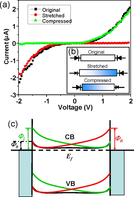
Figure 3a shows a transformation of a symmetric I-V curve to a rectifying behavior by straining. Both the forward bias and the reverse bias I-V curve of the as-fabricated device fit well with Eq. 6, which clearly demonstrates that there was symmetric Schottky barrier present at the contacts. Hence we suppose there was no axial strain in the wire as the device was first fabricated, although a kind of twist could be possible. The circuit diagram model of the device is a pair of back-to-back Schottky diodes, as illustrated in Fig. 3b. Under tensile strain, the piezoelectric potential at the right-hand side of this nanowire was lower [denoted by blue color in Fig. 3b], which raised the energy of the electrons in conduction band; thus, the Schottky barrier height became higher [denoted by a large diode symbol in Fig. 3b]. Since the positive piezoelectric potential was partially screened by free electrons, the Schottky barrier height at the left-hand side remained almost the same instead of being lowered. As a result, under positive bias voltage with the left-hand side positive, the current transport was determined by the reverse biased Schottky barrier at the right-hand side. While under the reverse biased voltage with the right-hand side positive, the current transport depended on the reverse biased Schottky barrier at the left-hand side, which had a much lower barrier height than the right-hand one. Experimentally, the device thus exhibited a rectifying behavior in the positive voltage region, and the I-V curve in the negative voltage region overlapped with that of the original curve without straining. By the same token, under compressive strain the device exhibited a rectifying behavior in the negative voltage region, and the I-V curve in the positive voltage region overlapped with that of the original curve without straining, as shown by the green line in Figs. 3a, 3c.
Figure 3.
Strain induced change of I-V characteristic from symmetric to asymmetric (diode). (a) Changes of transport characteristics of a Ag/ZnO-nanowire/Ag device from symmetric I-V characteristic (black) to asymmetric rectifying behavior when stretching (red) and compressing (green) the wire. (b) Circuit diagram models of the device in corresponding to the observed I-V curves, different sizes of diode symbol are used to illustrate the asymmetric Schottky contacts at the two ends of the nanowire. The blue side is the negative potential side, and the other side is the positive side. (c) Schematic energy band diagrams illustrating the changes of Schottky barriers from symmetric (black) to asymmetric under tensile strain (red) and compressive strain (green), in corresponding to the I-V curves in (a).
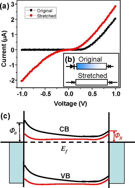
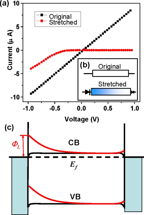
Figure 4a shows a case of changing the rectifying I-V characteristic to symmetric by tensile straining. The original rectifying I-V curve resulted from two back-to-back Schottky diodes with significantly different barrier heights. After stretching, Schottky barrier heights at both sides lowered to the same height as judged by the symmetric I-V curve shape. This is possible that the original as-fabricated device did have a built in strain, which created a piezoelectric potential in the wire, analogous to the strained case shown in Fig. 3. If the external strain applied in our experiment just canceled the original built-in strain, the wire became “strain-free” [Fig. 4b]. Thus, the Schottky barrier height originally contributed by the piezoelectric effect almost disappeared, resulting in a lowered barrier height at the left-hand side in Fig. 4b. Thus the equal barrier heights at the two ends gave a symmetric I-V [Fig. 4c].
Figure 4.
(a) Changes of transport characteristics of a Ag/ZnO-nanowire/Ag device from linear I-V curve (black) to rectifying feature when stretching (red) the wire. (b) Circuit diagram models of devices for the corresponded I-V curves. The blue side is the negative piezoelectric potential side. (c) Schematic energy band diagrams illustrating the changes in band structure of the contacts at the two ends of the nanowire under tensile strain.
We now consider other possible case related to Fig. 4. After stretching the wire, if the positive piezoelectric potential was at the low Schottky barrier side (right-hand side for example), the low barrier remained the same due to electron screen effect to the positive piezoelectric potential, while the high barrier side (left-hand side) became even higher, in which case the I-V curve would not be symmetric. Alternatively, if the positive piezoelectric potential was at the high Schottky barrier side, the high barrier would not be reduced due to the electron screen effect, while the low barrier side was raised, in which case the current will be rather small under both forward and reverse biased voltages due to high resistance at both contacts. Therefore, the original device should be compressive strained, which was canceled after applying a tensile strain.
Piezoelectric potential cannot only result in a switch between the symmetric I-V curve and rectifying behavior, but also can turn an Ohmic type into a diode. Figure 5 shows a case that a linear I-V transport behavior was converted into a rectifying behavior after applying a tensile strain. The negative piezoelectric potential at the left-hand-side of the wire after straining can introduce a Schottky barrier, while almost no change at the right-hand side. Under tensile straining, the I-V characteristic in the negative voltage region shows a lowered conductance, which could be due to the piezoresistance effect.
Figure 5.
(a) Changes of transport characteristics of a Ag/ZnO-nanowire/Ag device from symmetrical characteristic (black) to rectifying I-V curve (red) when stretching the wire. (b) Circuit diagram models of devices for the corresponded I-V curves. The blue side is the negative piezoelectric potential side. (c) Schematic energy band diagrams illustrating the changes in band structure of the contacts at the two ends of the nanowire under tensile strain.
CONCLUSION
In this paper, we have illustrated the theoretical and experimental evidence that shows the I-V transport property of a ZnO nanowire can be switched between asymmetric Schottky type and symmetric type by introducing strain. The fundamental mechanism lies in the creation of a piezoelectric potential distribution in ZnO nanowire under different straining conditions including stretching, compressing, twisting, and their combination. The transport process of metal-ZnO nanowire contacts can be modulated∕switched by the generated piezoelectric potential, resulting in a switch between the symmetric transport and asymmetric transport, or even turn an Ohmic contact type into a diode. Correctly manipulating the magnitude and distribution of piezoelectric potential in nanowires, a group of electronic devices can be fabricated. This is the fundamental principle of piezotronics.20
In practice, strain is unavoidable in the fabrication of nanowire based nanodevices due to reasons such as sample handling, substrate bending, substrate adhesion, and even solidification of metals. Such straining can introduce gigantic change in the transport properties of piezoelectric nanowires, such as ZnO, due to the creation of piezoelectric potential. The reported phenomena can also be extrapolated for nanowires of GaN, ZnS, CdS, and other wurtzite structured materials.
ACKNOWLEDGMENTS
Research supported by DARPA (Army∕AMCOM∕REDSTONE AR, Grant No. W31P4Q-08-1-0009), BES DOE (Grant No. DE-FG02-07ER46394), Air Force Office (Grant No. FA9550-08-1-0446), DARPA∕ARO Grant No. W911NF-08-1-0249, KAUST Global Research Partnership, World Premier International Research Center (WPI) Initiative on Materials Nanoarchitectonics, MEXT, Japan, Emory-Georgia Tech CCNE from NIH (Grant No. CA119338), and NSF (Grant Nos. DMS 0706436 and CMMI 0403671). Z.Y.G., Y.D.G., and P.F. thank the partial fellowship support by the China Scholarship Council (CSC) (Grant No. 20073020).
References
- Kamiya T. and Kawasaki M., MRS Bull. 33, 1061 (2008). [Google Scholar]
- Wang Z. L., Adv. Funct. Mater. 18, 3553 (2008). 10.1002/adfm.200800541 [DOI] [Google Scholar]
- Comini E., Baratoo C., Faglia G., Ferroni M., Vomiero A., and Sberveglieri G., Prog. Mater. Sci. 54, 1 (2009). 10.1016/j.pmatsci.2008.06.003 [DOI] [Google Scholar]
- Wang Z. L. and Song J. H., Science 312, 242 (2006). 10.1126/science.1124005 [DOI] [PubMed] [Google Scholar]
- Wang X. D., Zhou J., Song J. H., Liu J., Xu N. S., and Wang Z. L., Nano Lett. 6, 2768 (2006). 10.1021/nl061802g [DOI] [PubMed] [Google Scholar]
- Kind H., Yang H., Messer B., Law M., and Yang P., Adv. Mater. (Weinheim, Ger.) 14, 158 (2002). [DOI] [Google Scholar]
- Zhou J., Fei P., Gu Y. D., Mai W. J., Gao Y. F., Yang R. S., Bao G., and Wang Z. L., Nano Lett. 8, 3973 (2008). 10.1021/nl802497e [DOI] [PubMed] [Google Scholar]
- Zhou J., Gu Y. D., Fei P., Mai W. J., Gao Y. F., Yang R. S., Bao G., and Wang Z. L., Nano Lett. 8, 3035 (2008). 10.1021/nl802367t [DOI] [PubMed] [Google Scholar]
- Lao C. S., Liu J., Gao P. X., Zhang L. Y., Davidovic D., Tummala R., and Wang Z. L., Nano Lett. 6, 263 (2006). 10.1021/nl052239p [DOI] [PubMed] [Google Scholar]
- The impacts of Fermi energy pinning on the Schottky barrier height is still controversial for nanomaterials. Some calculations demonstrate that the Fermi-level pinning, no matter how strong, cannot control the device properties of metal-semiconductor contacts in the nanogeometry as that in a planar geometry, since the effects of the finite density of states throughout the bandgap of the semiconductor on the potential decays significantly within 2 nm at the metal-semiconductor interface. Leonard F. and Tersoff J., Phys. Rev. Lett. 84, 4693 (2000). 10.1103/PhysRevLett.84.4693 [DOI] [PubMed] [Google Scholar]
- Zhang Z. Y., Yao K., Liu Y., Jin C. H., Liang X. L., Chen Q., and Peng L. M., Adv. Funct. Mater. 17, 2478 (2007). 10.1002/adfm.200600475 [DOI] [Google Scholar]
- Hjelmstad K. D., Fundamentals of Structural Mechanics (Prentice-Hall, New Jersey, 1997). [Google Scholar]
- Cady W. G., Piezoelectricity (McGraw-Hill, New York, 1946). [Google Scholar]
- Gao Y. F. and Wang Z. L., Nano Lett. 7, 2499 (2007). 10.1021/nl071310j [DOI] [PubMed] [Google Scholar]
- Yang R. S., Qin Y., Dai L. M., and Wang Z. L., Nat. Nanotechnol. 314, 1 (2008). [Google Scholar]
- Lin Y. F. and Jian W. B., Nano Lett. 8, 3146 (2008). 10.1021/nl801347x [DOI] [PubMed] [Google Scholar]
- Gao Y. F. and Wang Z. L., Nano Lett. (2009). [DOI] [PubMed] [Google Scholar]
- Sze S. M., Physics of Semiconductor Devices (Wiley, New York, 1981). [Google Scholar]
- Fan Z. Y. and Lu J. G., Appl. Phys. Lett. 86, 032111 (2005). 10.1063/1.1851621 [DOI] [Google Scholar]
- Wang Z. L., Mater. Today 10, 20 (2007). 10.1016/S1369-7021(07)70076-7 [DOI] [Google Scholar]


