Abstract
We demonstrate rapid fabrication of submicrometer-diameter pores in borosilicate glass using femtosecond laser machining and subsequent wet-etch techniques. This approach allows direct and repeatable fabrication of high-quality pores with diameters of 400–800 nm. Such small pores coupled with the desirable electrical and chemical properties of glass enable sensitive resistive-pulse analysis to determine the size and concentration of macromolecules and nanoparticles. Plasma-enhanced chemical vapor deposition allows further reduction of pore diameters to below 300 nm.
Tiny pores in insulating substrates have been used as resistive-pulse sensors to detect and characterize microscale or nanoscale objects, such as DNA, nanoparticles, viruses, and small molecules [1–9]. Based on Coulter counting, this approach provides rapid, highly sensitive quantification of the size and concentration of a wide range of particles: When the particle to be detected passes through the pore, the resulting electrical resistive pulse exhibits a peak amplitude and half-width specific to the analyte or particle [10]. The peak amplitude for spheroid particles is directly proportional to the volume of a particle, and the frequency of the resistive pulses is proportional to the concentration of particles. In recent years, broad interest in label-free detection of minute quantities of biological or nanofabricated materials has brought increased interest in the fabrication of resistive-pulse sensors and analysis devices [1–9]. Pores have been fabricated in a variety of insulating materials, but glass is perhaps the ideal substrate, because it has excellent mechanical, thermal, optical, and electric properties; is inexpensive and readily available; and is inert to almost all solvents. However, precision machining of glass remains difficult. Here we use a femtosecond-pulsed (ultrafast) laser for high-precision machining of nanoscale sensors inside glass [11–16].
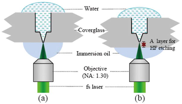
Submicrometer pore devices have been designed for a variety of biomedical sensing and screening applications [3–7]. Previously we introduced ultrafast laser machining for fabrication of submicrometer pores for detection of immune complexes and antibody-virus interactions [6,7]. These pores were machined using a femtosecond-pulsed laser focused onto glass by a high numerical aperture oil-immersion objective. This tight focusing enabled high precision, but the machining was hampered by the immersion oil: When the laser focus moved within ~1 μm of the glass-oil interface (Fig. 1), the laser created bubbles in the immersion oil that disrupted the focus of the laser; as a consequence, after one spot was ablated, it was necessary to wait for the bubble collapse before ablating the next spot. This severely limited the fabrication speed, and repeatability was suboptimal, with ~80% of the pores unsuitable for use. Here we demonstrate improved speed and reproducibility by combining direct laser ablation followed by wet etching.
Fig. 1.

(Color online) Schematic side view of laser machining geometry. (a) Direct ultrafast laser machining of a conical nanopore inside a coverglass as previously reported. (b) Greatly improved reproducibility and machining speed is achieved by terminating the pore 3 μm from the lower surface and postprocessing with an electrically monitored HF etch.
Figure 1 depicts a simplified diagram of the laser machining approach, and a detailed description can be found in [13]. The laser (1.5 kHz repeat frequency, 400 fs pulse width, and 527 nm wavelength halved by a frequency doubling KTP crystal) is focused through an inverted microscope with an oil-immersion objective of 1.3 NA into a borosilicate coverglass (Fisher-finest Premium Cover Glass) mounted on a three-dimensional nanomanipulation stage. The pore structures are comprised of a cylindrical shank and a conical tip. Since the machining tolerances are highest near the tip, we selected a higher pulse energy, 100–120 nJ/pulse, to machine the shank; this increases the material volume removed by each pulse, thereby increasing machining speed at the cost of decreased precision. The target coverglass is fixed onto the computer-controlled nanostage, allowing continuous translation, following a preprogrammed pattern, in circles with shrinking diameters. Translocation proceeds in steps with a size of 400 and 800 nm in the radial and azimuthal directions, respectively, relative to the direction of the laser. This strategy serially removes ablated material in a disk, after which the sample is moved by 800 nm in the vertical direction to machine the next layer, thus extending the length of the shank. At the last 5 μm of the shank, the size of the translation steps is reduced by 20%, placing subsequent pulses closer together to produce a smoother bottom surface. We then decrease the pulse energy to 10–20 nJ/pulse to machine a conical tip at the bottom of the shank. This energy is close to the laser damage threshold, thus reducing the subtracted volume per pulse and increasing machining precision. Accordingly the step sizes are reduced to 100 nm. The machining of the tip is similar to that of the cylinder except the diameter of the removed circular pattern of subsequent layers is decreased, producing a 30° conical pore terminating in a point 3 μm short of penetrating the entire coverglass thickness [Fig. 1(b)]. This protocol avoids producing bubbles in the immersion oil.
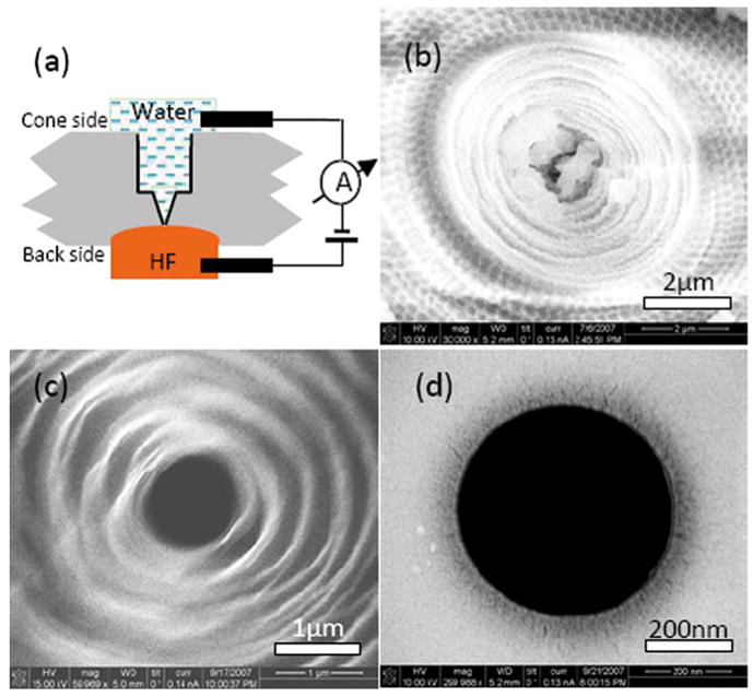
After laser machining, we use buffered hydrofluoric acid (BHF) to etch the 3 μm reserve layer. The coverglass, including the laser machined conical tip, is sandwiched between two teflon chambers, as schematically depicted in Fig. 2(a). One chamber contains deionized (DI) water and the other BHF. Platinum electrodes inserted into the fluid chambers are connected to a picoammeter, and a voltage of 500 mV is applied between the electrodes. In this way the onset of electrical continuity allows rapid detection of the opening of the pore by the BHF etch. A similar process has been used to prepare polyethylene terephthalate and polyimide pores [17].
Fig. 2.

(Color online) (a) Configuration of HF etch to complete the pore. HF etches away the lower surface of the glass (gray) until the tip of the conical pore is exposed. A picoammeter (Keithley 487) detects electrical continuity when the HF reaches the pore. (b) SEM of the cone side of a pore after laser machining (some machining debris remains at the center of the cone). (c) Cone side after HF etch (image is blurry owing to impaired secondary electrons collection). (d) Backside of the pore after HF etch.
Using Buffer HF Improved (Transene Inc.), etching proceeds at a rate of ~100 nm/minute. The cone side of the pore is also etched for 15 s to remove residual debris and to etch the conical tip to a smoother finish. After 20 min, the BHF is diluted fourfold, reducing the etch rate as the tip of the conical pore is approached. After 5–10 min, upon detection of a sudden increase in the current, the etch solution is removed, and the chamber is immediately flushed three times using DI water. This procedure results in pore diameters of 400–800 nm (e.g., Fig. 2). As shown in Fig. 2(b), debris sometimes remains in the pore after laser machining; however, the etch process removes this debris and smooths the cone [Fig. 2(c)]. After completion of the etch from the other side to generate an open pore through the coverglass, the backside picture [Fig. 2(d)] shows the sharp-edged, circular pore, ~490 nm in diameter.
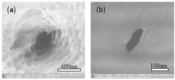
To make even smaller pores, necessary to detect small nanoparticles or single molecules, we apply plasma-enhanced chemical vapor deposition (PECVD, Group Sciences Inc., San Jose, Calif.) to shrink the pores. PECVD deposits a layer of silicon dioxide on the surface with thicknesses ranging from 100 to 1000 nm (deposition times of 8–74 s). The small opening of the pore (backside) is placed facing the reacting gases, and SiO2 deposition causes inward growth at the edges. Figure 3 shows this process used to shrink the diameter of a pore from ~460 to ~200 nm. Although the resulting shape is more irregular, the smaller size is suitable for detecting smaller particles.
Fig. 3.
(a) Cone side of a pore before the PECVD of SiO2. (b) Backside of the pore after 8 s of the PECVD shrinkage process.
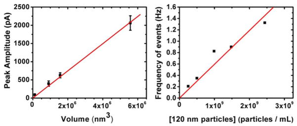
To examine the effectiveness of the nanopores for resistive-pulse sensing, we use nanoparticles (Bangs Labs) to characterize particle volume and concentration relationships to the peak amplitude and frequency of resistive pulses, respectively. A simple sensing device is constructed by mounting a coverglass with the pore [shown in Fig. 2(d)] onto a fluidic setup made of poly(dimethylsiloxane) (PDMS) [6,7]. Briefly, the glass containing a pore separates two solutions of Dulbecco’s Phosphate Buffered Saline containing 0.1% v/v Tween-20. Particles with diameters of 60, 120, 144, and 220 nm are added to one of the solutions at a concentration of 1×10⁹ particles/mL and used to determine the relation between peak amplitude and particle volume [Fig. 4(a)]. Under identical conditions, 120 nm particles are added to one compartment at increasing concentrations to correlate the event frequency with particle concentration.
Fig. 4.
(Color online) Calibration of a nanopore. (a) Average peak amplitude of resistive-pulse events from particles of diameters 60, 120, 144, and 220 nm passing through the 490 nm pore shown in Fig. 2(d). (b) Frequency of resistive pulse events versus the concentration of 120 nm particles. Linear regression fits were constrained to pass through the origin.
The diameter and length of the pore and the electrical noise in the recording system heavily influence the size detection limit of a resistive-pulse sensor [9]. Resistive-pulse events in conical nanopores typically contain frequency components of up to ~8 kHz [6–8]. Using the pore shown in Fig. 2(d) and an applied potential of 300 mV, the detection limits are 51, 53, and 57 nm diameter particles when filtering at cutoff frequencies of 10, 15, and 20 kHz, respectively. Here the threshold for event detection is 4 times the standard deviation of the noise from its mean baseline current.
In summary, we demonstrate a robust process to fabricate submicrometer-diameter pores using femto-second laser machining and electrically monitored wet etching with hydrofluoric acid. We use these pores to characterize the size and concentration of the nanoparticles and determine the size detection limits of a nanopore in a resistive-pulse sensing device. Further reduction of pore sizes by PECVD of silicon dioxide allows pores to meet the requirements for detecting very small (e.g., <51 nm) particles or molecules. Potential applications include high-sensitivity biomolecule sensors, sorting nanoparticles, and early detection of crystallization or precipitates; we are also investigating use in integrated lab-on-a-chip devices for biomedical diagnostics.
Acknowledgments
This work was supported by NIH R21EB006098 and R01GM072006 to A. J. Hunt and by NIH R01GM081705 to M. Mayer. The scanning electron microscope images were taken at Electron Microbeam Analysis Laboratory, University of Michigan.
References
- 1.Li J, Stein D, McMullan C, Branton D, Aziz MJ, Golovchenko JA. Nature. 2001;412:166. doi: 10.1038/35084037. [DOI] [PubMed] [Google Scholar]
- 2.DeBlois RW, Bean CP. Rev Sci Instrum. 1970;41:909. [Google Scholar]
- 3.Saleh OA, Sohn LL. Rev Sci Instrum. 2001;72:4449. [Google Scholar]
- 4.DeBlois RW, Uzgiris EE, Cluxton DH, Mazzone HM. Anal Biochem. 1978;90:273. doi: 10.1016/0003-2697(78)90032-5. [DOI] [PubMed] [Google Scholar]
- 5.Gu L, Braha O, Conlan S, Cheley S, Bayley H. Nature. 1999;398:686. doi: 10.1038/19491. [DOI] [PubMed] [Google Scholar]
- 6.Uram JD, Ke K, Hunt AJ, Mayer M. Angew Chem Int Ed. 2006;45:2281. doi: 10.1002/anie.200502862. [DOI] [PubMed] [Google Scholar]
- 7.Uram JD, Ke K, Hunt AJ, Mayer M. Small. 2006;2:967. doi: 10.1002/smll.200600006. [DOI] [PubMed] [Google Scholar]
- 8.Uram JD, Mayer M. Biosens Bioelectron. 2007;22:1556. doi: 10.1016/j.bios.2006.06.020. [DOI] [PubMed] [Google Scholar]
- 9.Uram JD, Ke K, Mayer M. ACS Nano. 2008 doi: 10.1021/nn/700322m. [DOI] [PubMed] [Google Scholar]
- 10.Bayley H, Martin CR. Chem Rev. 2000;100:2575. doi: 10.1021/cr980099g. [DOI] [PubMed] [Google Scholar]
- 11.Glezer EN, Milosavljevic M, Huang L, Finlay RJ, Her TH, Callan JP, Mazur E. Opt Lett. 1996;21:2023. doi: 10.1364/ol.21.002023. [DOI] [PubMed] [Google Scholar]
- 12.Perry MD, Stuart BC, Banks PS, Feit MD, Yanovsky V, Rubenchik AM. J Appl Phys. 1999;85:6803. [Google Scholar]
- 13.Joglekar AP, Liu H, Spooner GJ, Meyhofer E, Mourou G, Hunt AJ. Appl Phys B. 2003;77:25. [Google Scholar]
- 14.Li Y, Itoh K, Watanabe W, Yamada K, Kuroda D, Nishii J, Jiang YY. Opt Lett. 2001;26:1912. doi: 10.1364/ol.26.001912. [DOI] [PubMed] [Google Scholar]
- 15.An R, Li Y, Dou YP, Yang H, Gong QH. Opt Express. 2005;13:1855. doi: 10.1364/opex.13.001855. [DOI] [PubMed] [Google Scholar]
- 16.Ke K, Hasselbrink EF, Hunt AJ. Anal Chem. 2005;77:5083. doi: 10.1021/ac0505167. [DOI] [PubMed] [Google Scholar]
- 17.Siwy Z, Apel P, Baur D, Dobrev DD, Korchev YE, Neumann R, Spohr R, Trautmann C, Voss K. Surf Sci. 2003;532–535:1061. [Google Scholar]


