Abstract
The authors introduce a technique for three-dimensional (3D) imaging of the light transmitted through periodic nanoapertures using a scanning probe to perform optical sectioning microscopy. For a 4×4 nanohole array, the transmitted light displays intensity modulations along the propagation axis, with the maximum intensity occurring at 450 μm above the surface. The propagating fields show low divergence, suggesting a beaming effect induced by the array. At distances within 25 μm from the surface, they observe subwavelength confinement of light propagating from the individual nanoholes. Hence, this technique can potentially be used to map the 3D distribution of propagating light, with high spatial resolution.
The interaction of light with nanoapertures in metallic films produces interesting effects that resemble the properties of traditional optical elements, such as chromatic filters1–11 and lenses.12–14 The optical characteristics of these perforated films are created by the interference of the transmitted light with surface modes, plasmon polaritons 1–10 and/or diffracted evanescent waves.11 A recent review is given in Ref. 15. Experimental methods used for imaging the transmittivity of subwavelength apertures utilize near-field scanning optical microscopy (NSOM). NSOM has been used to characterize the optical properties of a variety of nanoapertures and various kinds of arrays of nanoapertures.12,16,17 However, unlike the surface nearfields, the three-dimensional (3D) far-field light distribution from nanoapertures (nanostructures) have not been widely explored experimentally, and hence there is little data available to confirm theoretical predictions. In this letter, we present an experimental approach to map the 3D spatial intensity distribution of light transmitted through nanohole arrays, at distances from the surface to 1000 μm above, by using a NSOM tip for high resolution optical mapping of the far-field radiation.
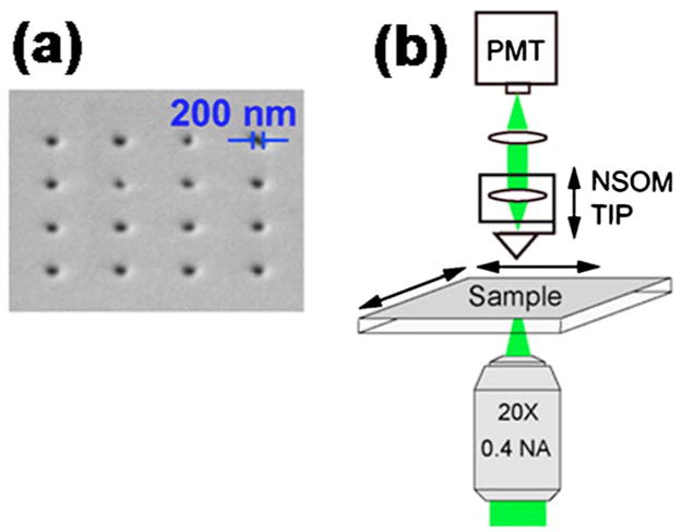
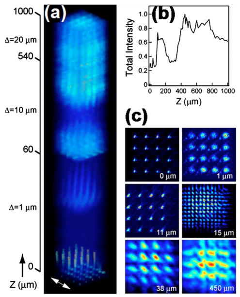
We investigated the light fields transmitted through a 4×4 nanohole array in a silver film supported by a glass substrate [Fig. 1(a)]. The array is illuminated with 514.5 nm laser light, and imaging is performed with a NSOM (WITec α-300S, GmbH) in collection mode [Fig. 1(b)]. The NSOM is used to obtain the light field distribution above the array in a manner similar to optical sectioning microscopy. To accomplish this, the NSOM tip is initially positioned at the surface, and a traditional NSOM image is obtained. Then, the aperture is positioned at varying distances above the surface up to 1000 μm, and the same area is imaged. As shown in Fig. 2(a), the 3D light intensity distribution is very complex and exhibits many interesting features. We note that the intensity does not decay sharply as one may initially expect but actually propagates along the optical axis well into the far field—this was a surprising observation. Also, the propagating field does not decay monotonically but is modulated in a striking manner [Fig. 2(b)]. From a broad viewpoint, the intensity distribution consists of three minima and four maxima. Interestingly, the maximum light intensity does not occur near the surface apertures but at the image plane 450 μm away. The intensity minima are unusual, and demonstrate that these nanohole arrays can cause the propagating light to destructively interfere, creating “dark zones” that can extend as much as 30 μm along the propagation axis [Figs. 2(a) and 3, 20–30 μm]. This extended dark zone may have eluded any previous attempts to examine the light fields at significant distances from the surface.
FIG. 1.

(a) (Color online) Scanning electron micrograph of the 4×4 nanohole array. Nanoholes were made by focused ion beam milling into a 200 nm thick silver film thermally deposited onto a 170 μm thick glass coverslip. Average hole diameter is 200 nm and center-to-center spacing is 2060 nm. (b) Schematic of the NSOM setup. A long working distance (3.8 mm) objective is used to focus the laser onto the upper silvered sample surface and aligned to the NSOM aperture. Imaging is performed by raster scanning the sample, with the objective and NSOM tip held at a fixed position. Light collected by the NSOM tip is focused onto a photomultiplier tube detector. The NSOM tip height is varied to obtain the 3D light intensity distribution.
FIG. 2.
(Color online) Transmission intensity along the Z axis. (a) False color 3D intensity distribution of light transmitted through the 4×4 nanohole array. Scan resolution in the XY plane is 50 nm over the 10 ×10 μm2 area. For optical sectioning, the Z height position of the NSOM tip was incremented by ΔZ=1 μm from 0 to 60 μm, ΔZ=10 μm from 70 to 540 μm, and ΔZ=20 μm from 560 to 1000 μm. The incident light polarization is along the X axis (white double arrow). (b) Total light intensity for each image plane as a function of the NSOM tip distance from the surface. (c) Self-normalized XY plane images at selected Z heights.
FIG. 3.
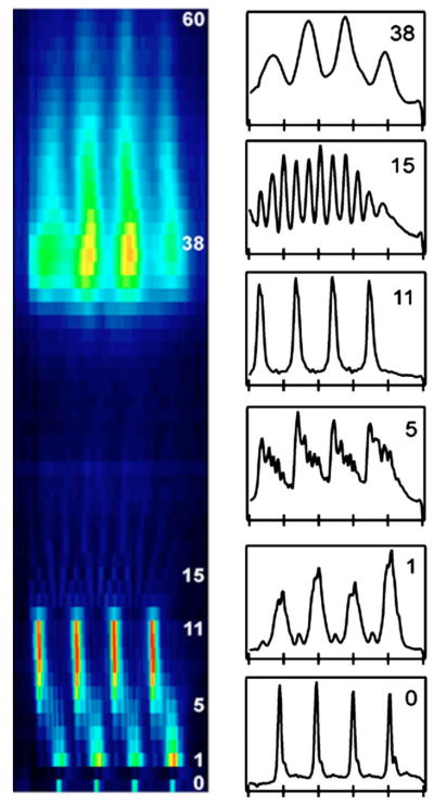
(Color online) (Left) Projection of the 3D light intensity distribution along the XZ plane. The NSOM tip distance, Z (μm), from the surface is given on the right of the image. Each area scan is separated by ΔZ=1 μm, except for the second scan which was taken at Z=500 nm above the surface and the third scan which was at Z=1 μm. (Right) Line intensity profiles obtained from the XZ image at several Z positions as given in the upper right of the plots.
Another interesting feature of the light intensity distribution volume is that it appears to have beaming characteristics; i.e., it does not diverge outside of the array boundary—although within the array boundary, the 16 individual nanoholes appear smeared at distances greater than 60 μm from the surface [Fig. 2(c)]. Beaming of light has also been observed for single nanohole apertures that are surrounded by concentric, corrugated rings12 and nanoslits flanked by periodic nanostructures.12–14 In these geometries, the interference of the surface plasmon modes with the transmitted light acts similar to a lens to focus the light. However, there is a lack of both experimental and theoretical investigations of the light field distribution at large distances (>100 μm) from the surface.
At distances below 60 μm from the surface, the 16 nanoholes are easily resolvable for at least four different revival image planes, as shown in Fig. 2(c). At other image planes such as Z=15 μm, the image displays a higher periodicity than the surface image, which was unexpected and hence highly intriguing. For clarity, Fig. 3 displays a projection of the 3D intensity volume onto the XZ plane, which is produced by summing the pixel values along the Y axis. The revival images are similar to the optical Talbot self-imaging effect.18–22 This phenomenon was discovered by Talbot in 1836 and can be observed with periodic structures (e.g., gratings) illuminated with coherent light. With an ideal (infinite) periodic grating, revival images of the structure reappear at the so-called Talbot distances, ZT(n) =n2d2/λ, where n is an integer, d is the periodicity of the structure, and λ is the illumination wavelength. Significant variation in the intensity distribution both transversely and along the direction of propagation has been observed at distances located in between Talbot planes for coherent array beams from carbon dioxide waveguide lasers, which has been attributed to destructive and constructive interferences of the coherent array emission.20 Very recently, the plasmon Talbot effect has been reported on metallic substrates that leads to focusing of light along the propagation axis (z axis) by quasiperiodic arrays, and the in-plane (along the y axis) focusing of light by linear nanohole arrays.21,22 For the nanohole array used in this study, d=2060 nm=4λ, and the first Talbot image plane is expected to occur at ZT(1) =32λ=16.5 μm with 514.5 nm light. Additional images of the nanohole array should also reappear at integer multiples of the Talbot distances: 33.0, 49.4, 65.9 μm, etc. As can be seen from Fig. 3, this trend was not observed with our nanohole array. Specifically, the nanohole array produced “imagelike” revivals at Z planes: 1, 11, and 38 μm [Figs. 2(c) and 3]. However, a strong Talbot effect would not be expected for a 4×4 hole array because it is not an ideal periodic structure. Furthermore, the subwave-length dimensions of the apertures and the interference between the surface plasmon modes (localized and polaritons) with the transmitted light can significantly alter the free-space diffraction that produces Talbot self-imaging. Nonetheless, we note that the silver nanohole array used in this study can produce a self-imaging phenomenon with “Talbot-like” characteristics. Although we do not yet fully understand the exact reasons behind our observations, we believe that it is the complex interplay of the destructive and constructive interferences of the coherent array emission combined with the plasmonic nature of the interaction of our silver nanohole array with the incident laser that causes the interesting observations presented in Figs. 2 and 3.
Additionally, the nanohole array also displays a fractional Talbot-like effect.18,19,21,23 Images with an increase in periodicity of the original structure occur at fractional Talbot planes ZT/2m, where m is an integer that reflects the periodicity. For odd values of m, the revival images are shifted by 1/2 periods relative to the original structure. Fractional image revivals were observed with our nanohole array at Z=11 μm, which show a periodicity of m=1 (shifted by 1/2 period), and at Z=15 μm, the image displays a periodicity of m=2 [Figs. 2(b) and 3]. Higher order periodicities may also be present but were not evident in our experimental setup.
The fractional image plane at Z=11 μm shows very unique optical features. Particularly interesting are the subwavelength dimensions of the light propagating from each nanohole, comparable to the diameter of the apertures. For comparison, line intensity profiles (along the X axis) at key image planes are provided in Fig. 3. At the surface, the line profiles of the nanoholes yield a full width at half maximum (FWHM) value of 124±5 nm, and at 11 μm, the FWHM=213±9 nm—the light intensity at this plane is about twice that at the surface. Notice that the propagating light is very well registered and similar in intensity from 8–11 μm, indicating low divergence. This feature shows considerable promise for the development of an optical microscope with subwavelength resolution, similar to a NSOM, but without the restriction of the illumination source being in contact with the sample because the light propagates into the far field. The parameters that define the propagating light fields are currently under investigation.
Successful realization of future nanophotonic devices will rely on the push-pull interactions between experiment and theory. Although there are many theoretical reports calculating the far-field light profiles around nanostructures, there is little experimental evidence to validate these predictions. To address this concern, we propose to utilize scanning probe microscopy. The typical aperture size of NSOM probes is less than 100 nm in diameter, which offers greater lateral (X-Y) resolution compared to conventional light microscopy. Also, the optical “depth of focus” for a NSOM tip is approximately 100–200 nm. Thus, optical sectioning using a NSOM tip affords superior axial resolution, compared to 1–2 μm obtained by confocal microscopy. Hence, we believe that scanning aperture microscopy can be used as a general method to probe interactions between light and matter and the resulting far-field radiation profile.
Acknowledgments
This work was supported by the NIH (Nos. RR-08119, EB-000682, EB-006521 and HG-002655), and by the Penn State University MRI NanoFab Network and the NSF Cooperative Agreement No. 0335765, NNIN, with Cornell University. The authors thank G. Lavallee, J. McIntosh, and J. Stitt for their technical assistance with nanofabrication and characterization.
Contributor Information
Mustafa H. Chowdhury, Center for Fluorescence Spectroscopy, Department of Biochemistry and Molecular Biology, University of Maryland School of Medicine, 725 West Lombard Street, Baltimore, Maryland 21201
Jeffrey M. Catchmark, Department of Agricultural and Biological Engineering, The Pennsylvania State University, 109 Agricultural Engineering Building, University Park, Pennsylvania 16802
Joseph R. Lakowicz, Center for Fluorescence Spectroscopy, Department of Biochemistry and Molecular Biology, University of Maryland School of Medicine, 725 West Lombard Street, Baltimore, Maryland 21201.
References
- 1.Ebbesen TW, Lezec HJ, Ghaemi HF, Thio T, Wolff PA. Nature (London) 1998;391:667. [Google Scholar]
- 2.Degiron A, Lezec HJ, Barnes WL, Ebbesen TW. Appl Phys Lett. 2002;81:4327. [Google Scholar]
- 3.Barbara A, Quémerais P, Bustarret E, Lopez-Rio T. Phys Rev B. 2002;66:161403. [Google Scholar]
- 4.Klein Koerkamp KJ, Enoch S, Segerink FB, van Hulst NF, Kuipers L. Phys Rev Lett. 2004;92:183901. doi: 10.1103/PhysRevLett.92.183901. [DOI] [PubMed] [Google Scholar]
- 5.Degiron A, Ebbesen TW. Opt Express. 2004;12:3694. doi: 10.1364/opex.12.003694. [DOI] [PubMed] [Google Scholar]
- 6.Prikulis J, Hanarp P, Olofsson L, Sutherland D, Käll M. Nano Lett. 2004;4:1003. [Google Scholar]
- 7.Gordon R, Brolo AG, McKinnon A, Rajora A, Leathem B, Kavanagh KL. Phys Rev Lett. 2004;92:037401. doi: 10.1103/PhysRevLett.92.037401. [DOI] [PubMed] [Google Scholar]
- 8.Degiron A, Ebbesen TW. J Opt A Pure Appl Opt. 2005;7:S90. [Google Scholar]
- 9.Lalanne P, Rodier JC, Hugonin JP. J Opt A, Pure Appl Opt. 2005;7:422. [Google Scholar]
- 10.DiMaio JR, Ballato J. Opt Express. 2006;14:2380. doi: 10.1364/oe.14.002380. [DOI] [PubMed] [Google Scholar]
- 11.Lezec HJ, Thio T. Opt Express. 2004;12:3629. doi: 10.1364/opex.12.003629. [DOI] [PubMed] [Google Scholar]
- 12.Lezec HJ, Degiron A, Devaux E, Linke RA, Martin-Moreno L, Garcia-Vidal FJ, Ebbesen TW. Science. 2002;297:820. doi: 10.1126/science.1071895. [DOI] [PubMed] [Google Scholar]
- 13.Wang B, Wang GP. Appl Phys Lett. 2006;88:013114. [Google Scholar]
- 14.Lin DZ, Chang CK, Chen YC, Yang DL, Lin MW, Yeh JT, Liu JM, Kuan CH, Yeh CS, Lee CK. Opt Express. 2006;14:3503. doi: 10.1364/oe.14.003503. [DOI] [PubMed] [Google Scholar]
- 15.Genet C, Ebbesen TW. Nature (London) 2007;445:39. doi: 10.1038/nature05350. [DOI] [PubMed] [Google Scholar]
- 16.Yin L, Vlasko-Vlasov VK, Rydh A, Pearson J, Welp U, Chang SH, Gray SK, Schatz GC, Brown DB, Kimball CW. Appl Phys Lett. 2004;85:467. [Google Scholar]
- 17.Hohng SC, Yoon YC, Kim DS, Malyarchuk V, Müller R, Lienau Ch, Park JW, Yoo KH, Kim J, Ryu HY, Park QH. Appl Phys Lett. 2002;81:3239. [Google Scholar]
- 18.Noponen E, Turunen J. Opt Commun. 1993;98:132. [Google Scholar]
- 19.Guérineau N, Di Mambro E, Primot J. Opt Express. 2003;11:3310. doi: 10.1364/oe.11.003310. [DOI] [PubMed] [Google Scholar]
- 20.Baker HJ, Hall DR, Hornby AM, Morley RJ, Taghizadeh MR, Yelden EF. IEEE J Quantum Electron. 1996;32:400. [Google Scholar]
- 21.Dennis MR, Zheludev NI, de Abajo FJG. Opt Express. 2007;15:9692. doi: 10.1364/oe.15.009692. [DOI] [PubMed] [Google Scholar]
- 22.Huang FM, Zheludev N, Chen Y, de Abajo FJG. Appl Phys Lett. 2007;90:091119. [Google Scholar]
- 23.Leger JR, Swanson GJ. Opt Lett. 1990;15:288. doi: 10.1364/ol.15.000288. [DOI] [PubMed] [Google Scholar]


