Abstract
Optical biosensing based on fluorescence detection has arguably become the standard technique for quantifying extents of hybridization between surface-immobilized probes and fluorophore-labeled analyte targets in DNA microarrays. However, electrochemical detection techniques are emerging which could eliminate the need for physically bulky optical instrumentation, enabling the design of portable devices for point-of-care applications. Unlike fluorescence detection, which can function well using a passive substrate (one without integrated electronics), multiplexed electrochemical detection requires an electronically-active substrate to analyze each array site and benefits from the addition of integrated electronic instrumentation to further reduce platform size and eliminate the electromagnetic interference that can result from bringing non-amplified signals off chip. We report on an active electrochemical biosensor array, constructed with a standard complementary metal-oxide-semiconductor (CMOS) technology, to perform quantitative DNA hybridization detection on chip using targets conjugated with ferrocene redox labels. A 4×4 array of gold working electrodes and integrated potentiostat electronics, consisting of control amplifiers and current-input analog-to-digital converters, on a custom-designed 5×3 mm2 CMOS chip drive redox reactions using cyclic voltammetry, sense DNA binding, and transmit digital data off chip for analysis. We demonstrate multiplexed and specific detection of DNA targets as well as real-time monitoring of hybridization, a task that is difficult, if not impossible, with traditional fluorescence-based microarrays.
Keywords: DNA detection, CMOS, electrochemical biosensor array
1. Introduction
High-throughput, multiplexed DNA analysis is usually performed using a “microarray”, a passive substrate (such as a glass slide) on which single-stranded DNA (ssDNA) “probe” molecules arranged in a regular pattern bind to (or “hybridize” with) complementary fluorophore-labeled “target” molecules in an unknown analyte solution (Lipshutz et al., 1995; Schena et al., 1995). After non-hybridized targets are removed from the array through a washing step, the locations of hybridized targets on the microarray surface are measured with a scanner consisting of one or more sources for excitation and a photomultiplier tube or charge-coupled device camera to detect the emitted light. Relative expression levels of bound targets at different array sites can then be quantified from the resulting image.
Although fluorescence-based microarray platforms have very low detection limits [capable of measuring surface-bound target coverages down to 106 cm−2 (Schena, 2003)], the optical instrumentation they require is physically bulky, defying portability for point-of-care applications. In addition, hybridization cannot be monitored in real-time because it is impossible to distinguish between unbound targets in solution and those that have hybridized on the surface as both will fluoresce when imaged. The ability to perform real-time sensing could increase assay throughput and improve detection limits through temporal averaging (Vikalo et al., 2006).
Emerging electrochemical techniques promise higher degrees of integration by eliminating the need for light as an intermediary for sensing. Electrochemical DNA sensors measure electronic activity that results from the hybridization of ssDNA targets to probes immobilized on metallic (Herne and Tarlov, 1997; Steel et al., 1998) or carbon (Millan et al., 1994) “working” electrodes (WEs) immersed in an electrolyte (Gooding, 2002; Wang, 2002). The nature of this electronic activity depends on the sensing methodology used but often involves the introduction of electrochemically-active labels on the target DNA. A potentiostat applies a desired input voltage to the electrochemical cell and measures the resulting current passing through the WE.
Because of limited wiring resources (Drummond et al., 2003), the construction of high-density arrays based on electrochemical sensing requires electronically-active substrates to perform multiplexed detection. A commercially-available system from CombiMatrix (Mukilteo, WA, USA) consists of a complementary metal-oxide-semiconductor (CMOS) microarray chip containing individually-addressable microelectrode sites and an external (off-chip) reader containing actuation and measurement circuitry (Ghindilis et al., 2007). Real-time sensing is not possible with this system because hybridized targets are only conjugated with electroactive labels after hybridization has occurred. Other pioneering work in label-based CMOS DNA arrays with on-chip detection circuitry includes sensing using redox-cycling (Hofmann et al., 2002; Schienle et al., 2004) and intercalation-based (Gemma et al., 2006) techniques. However, the former of these methods did not support generalized potentiostat functionality and neither demonstrated real-time monitoring of hybridization with the ability to directly measure surface target coverages.
In this work, we explore the limits of form-factor achievable with electrochemical detection by constructing an integrated sensor array directly on an electronically-active, CMOS substrate. The active CMOS biosensor described here includes an array of WEs and full potentiostat electronics, including control-loop amplifiers, current-input analog-to-digital converters (ADCs), and data-processing circuitry. Unwanted electromagnetic interference effects that often result form bringing unamplified signals to off-chip sensing electronics are eliminated. The redox molecule ferrocene (an electroactive species that undergoes reduction or oxidation according to the applied potential) is covalently attached to the target DNA. Because only labeled target molecules localized immediately at the electrode surface allow facile electron transfer, no washing step is required and DNA hybridization can be monitored in real time.
2. Methods
2.1. Electrochemical DNA sensing
We perform quantitative, real-time electrochemical measurement of surface hybridizations. The targets are covalently modified with N-(2-ferrocene-ethyl) maleimide redox labels which are known to be chemically stable and are electrochemically reversible (Chahma et al., 2004). Electroactive labeling has been recognized as an alternative to the use of radioactive isotopes for nucleic acid sequencing and sensing (Ihara et al., 1996). For example, ferrocene (Fc) redox labels have previously been used to study the thermodynamics of DNA probe binding (Ihara et al., 1996) and to perform label-based detection of RNA hybridization (Di Giusto et al., 2004), among various other applications (Fan et al., 2003; Yu et al., 2001). Fc undergoes the redox reaction Fc ↔ Fc+ + e over a well-defined potential range. In this work, Fc labels are used to provide a quantitative measure of the extent of surface hybridization by integrating the resulting current and relating it to a surface target coverage.
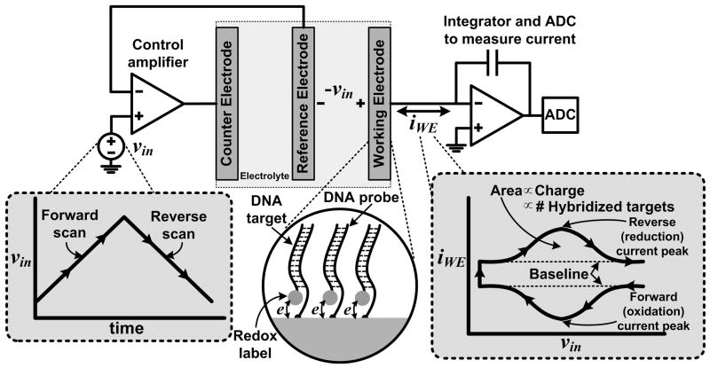
Electrochemical measurements are normally carried out using a potentiostat—an electronic control system that applies a desired potential to an electrochemical cell and simultaneously measures the movement of charge through the cell that accompanies electrochemical reactions and charging currents at the electrode-electrolyte interface. A standard experimental electrochemical cell consists of three electrodes immersed in an electrolyte: a WE, at which the reaction of interest occurs and to which DNA probes are attached, a “reference” electrode (RE) to hold the buffer at a stable potential, and a “counter” electrode (CE) which acts as the source or sink of the cell current. The potentiostat electronics are shown in Fig. 1, where the high gain of the control amplifier (implemented as a single operational amplifier) on the left ensures that the potential at the WE interface (relative to the RE) operates at a desired input level vin. The amplifier on the right measures the current flowing through the WE iWE by integrating it onto a capacitor and then sampling it with an ADC.
Fig. 1.
Electrochemical quantitation of ferrocene-labeled DNA targets hybridized to probes on the surface of a working electrode using cyclic voltammetry. A potentiostat applies vin to the WE interface and measures the redox current iWE using an integrator and an ADC. The shape of iWE as a function of vin is characteristic of the response from an electroactive surface species.
We use cyclic voltammetry (CV), a classical electrochemical measurement technique, to drive the redox reactions associated with the Fc labels. Using this technique, vin starts at zero, is ramped up to +0.35 V (versus a standard Ag/AgCl/3 M NaCl RE) at a scan rate ν of 60 V s−1, and is then ramped back down to zero at the same rate. Fc labels attached to hybridized targets are oxidized during the forward scan and are reduced in the reverse scan, as displayed in Fig 1. The overall shape of iWE shown in the figure is attributed to the fact that Fc is a surface (rather than a bulk) redox species (Bard and Faulkner, 2001). The baseline (charging) current level is due to the WE interfacial “double-layer” capacitance CWE, and is equal to ±CWE ν. The surface density of hybridized probe-target pairs on the WE can be determined by integrating the area enclosed by the Fc redox (Faradaic) current after subtraction of background charging (non-Faradaic) contributions, and then dividing the result (in Coulombs) by the magnitude of the electronic charge and by the WE area.
2.2. CMOS-integrated biosensor design
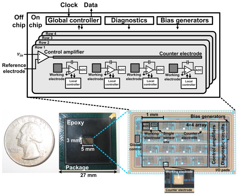
Our integrated biosensor array is fabricated using a commercial CMOS process (Taiwan Semiconductor Manufacturing Company, Hsinchu, Taiwan) that has a minimum feature size of 0.25 μm and that operates at a nominal power-supply voltage of 2.5 V. The overall system architecture and chip photograph are shown in Fig. 2. The 5×3 mm2 chip is comprised of a 4×4 array of sensor sites which operate simultaneously. Each site contains a square WE, a 10-bit integrating ADC (Johns and Martin, 1997) to sense the current flowing through the WE, and digital circuitry to set ADC control signals and transmit the digital data off chip. The ADCs can be programmed to sense currents ranging from 100 pA to 250 nA at sampling rates up to 10 kHz, which is sufficient for our label-based detection method. The top-row WEs have side lengths of 100 μm, with subsequent rows having side lengths of 90, 80, and 70 μm. This variation allows us to study the effect of electrode area on signal level. Each row of four WEs shares an integrated 2500×15 μm2 CE that is attached to the output of a low-noise control amplifier (with a gain of 87 dB). The inputs to this amplifier connect to an off-chip Ag/AgCl/3 M NaCl RE (RE-5B, Bioanalytical Systems, West Lafayette, IN, USA) and an external signal generator that, along with the WEs and supporting circuits, form a standard potentiostat. The chip also includes diagnostic circuits for ADC testing, dc bias generators, as well as a digital global-control unit. More details on the electronics can be found in (Levine et al., 2007).
Fig. 2.
The active biosensor array for DNA detection has been designed using a 0.25 μm CMOS technology, measures 5×3 mm2, and contains potentiostat electronics with sixteen sensing sites, each having an integrated ADC to measure currents produced by electrochemical reactions occurring at the on-chip WEs. The overall system architecture, chip surface with a magnified view of a WE and CE after Ti-Au deposition, and chip packaging are shown.
2.3. Chip post-processing, packaging, and experimental setup
CMOS technologies use stacked metal layers [connected vertically by tungsten (W) “vias”] to route electrical signals and form transistor interconnects and are usually passivated with SiO2 and Si3N4 at the chip surface. To construct on-chip WEs, we specify square openings in the passivation layers at the time of chip manufacturing, exposing the top-metal layer at various pre-defined locations. Conventional CMOS processes normally employ Al for this layer, which is highly electroactive and can easily corrode when exposed to an electrolyte. Therefore, we selectively remove the Al at these locations using a phosphoric-acid wet etch following chip fabrication, leaving the W vias exposed. We then deposit a 200-nm-thick layer of Au (with a 20-nm-thick Ti adhesion layer) through electron-beam evaporation on the exposed electrode sites followed by a lift-off process. We use Au as the electrode metal because it is relatively electrochemically inactive and is easily modified by self-assembly of well-ordered monolayers of thiol, sulfide, or disulfide compounds through Au-S bonding (Ulman, 1996). As a result, thiolated DNA probes can be bound strongly to Au surfaces. The on-chip CEs are constructed in a similar fashion as the WEs. This method of surface electrode array fabrication provides a significant advance over previous methods in which a complete CMOS back-end process is required (Hofmann et al., 2002). Because our procedure is more easily implemented in pre-existing CMOS technologies, it translates to much lower fabrication costs and complexity.
To enable electrochemical testing of the CMOS biosensor array and external interfacing, the chip is mounted in a 272-pin, 27×27 mm2 ball-grid array (BGA) package with its surface partially exposed, as displayed in Fig. 2. The metal bond wires connecting the input-output (I/O) pads along the chip perimeter to the BGA package are encapsulated using a chemically-resistant epoxy (Hysol, Henkel, Düsseldorf, Germany) to shield them from electrolyte exposure. Further details about the experimental setup, along with our data processing and analysis methodologies, are included in the supplementary material.
2.4. DNA oligonucleotide sequences
The sequences of the 3′-end thiolated 20-mer DNA oligonucleotide probes (MWG-Biotech, High Point, NC, USA) used in our CMOS biosensor array experiments are as follows: P1 5′-TTT TAA ATT CTG CAA GTG ATJ-3′ (from Homo sapiens retinoblastoma 1 mRNA) and P2 5′-TTT TTT TCC TTC CTT TTT TTJ-3′; where J represents a thiol group. The target sequences (MWG-Biotech) are as follows: T1 5′-FcCAC TTG CAG AAT TTA AAA-3′ and T2 5′-FcAAA AAG GAA GGA AAA AAA-3′. Sequences P1 and T1, and P2 and T2, are pairwise complementary, respectively. These model sequences were chosen in order to demonstrate the functionality of our active CMOS bionsensor array platform and to allow comparison with off-chip electrochemical experiments using similar sequences.
2.5. Ferrocene redox label preparation and DNA target labeling
Our Fc redox label synthesis method is similar to that reported previously (Di Gleria et al., 1996) and can be found in the supplementary material, together with details on its conjugation with DNA target molecules.
2.6. Chip surface preparation
Organic contaminants on the chip surface are first removed by placing the packaged chip in an UV/ozone cleaning system (Vig, 1985) (T10x10/OES, UVOCS, Montgomeryville, PA, USA) for 5 min followed by thorough rinsing in deionized water (18.2 MΩ cm). Next, we construct a layer of ssDNA probes at each WE by incubating the surface of the chip in 1 M MgCl2 solution containing 500 nM probe for 30 min. This provides a probe surface density of approximately 8×1012 cm−2, which is determined from a set of calibration measurements performed off chip (Gong and Levicky, 2008). After probe immobilization, we incubate the chip in a 1 mM mercaptopropanol (MCP) solution (Aldrich) for 90 min which forms a self-assembled monolayer on the Au WEs. This passivates the WE surfaces and reduces non-specific binding of probes and targets (Herne and Tarlov, 1997). We run all our CV experiments in 7 ml of 1 M PPB (pH 7.4), made by combining appropriate amounts of K2HPO4 and KH2PO4 in water.
3. Results and discussion
3.1. DNA hybridization detection
Fig. 3 shows a typical output from the ADC measured at one of the 100 μm WEs in the array, functionalized with probe P1, approximately 50 min after 50 nM of target T1 is introduced to the system. The current peaks due to the Fc redox reactions are evident above the charging current level, indicating hybridization between P1 and T1. Hysteresis causes the forward and reverse charging currents to differ somewhat. Based on the average charging current, the WE interfacial capacitance is measured to be approximately 7 μF cm−2, which is in the expected range for an MCP-modified Au electrode at this DNA coverage and buffer ionic strength (Shen et al., 2006).
Fig. 3.
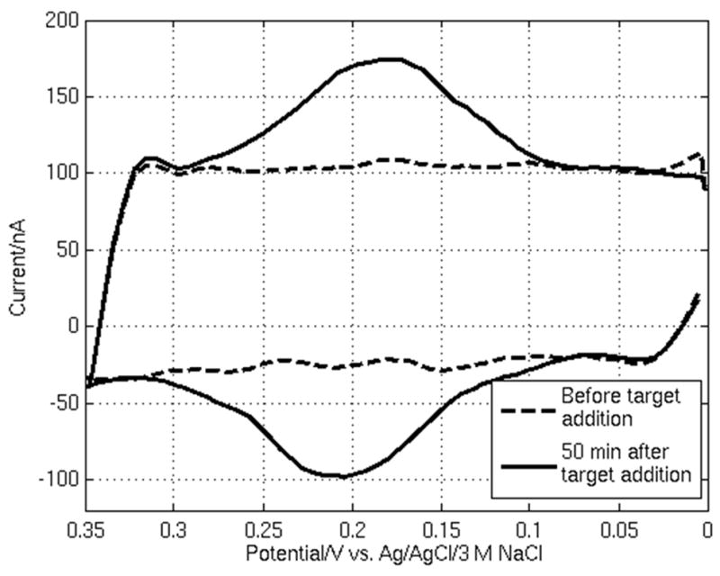
A typical CV measurement using the active CMOS biosensor array in which the charging current, before DNA target is added to the buffer, is shown along with the sensor response from hybridization, 50 min after target addition, at one 100 μm WE.
Experimental data showing that the peak current level (average of forward and reverse peaks after background subtraction) increases linearly with scan rate, as predicted by theory for a surface redox species (Bard and Faulkner, 2001), has been included in the supplementary material. This confirms that the signal current originates from surface-hybridized targets and not diffusing species in solution. The measured linear dependence of peak current on WE area, as predicted by theory, is also shown in the supplementary material.
For all measurements, we found that the 2.5 V supply limited the potential range over which the on-chip control amplifiers could operate. As a result, the on-chip CEs were bypassed and an external discrete operational amplifier (AD8628, Analog Devices, Norwood, MA, USA), that could operate up to 3 V, was used to drive the RE and an off-chip Pt-wire CE. This issue can be resolved in the future by designing the control amplifiers using thick-gate-oxide transistors, which can be operated up to 3.3 V in our current CMOS process. The on-chip area requirements and system performance are not expected to change significantly with this modification.
3.2. Target concentration series
In principle, our integrated platform enables real-time quantitation of surface-hybridized targets in a multiplexed fashion, allowing large-scale optimization of parameters affecting hybridization in diagnostic assays including probe coverage, target concentration, probe and target sequence, buffer ionic strength, and temperature (Levicky and Horgan, 2005). As a first step in this direction it is important to examine the relationship between the concentration of DNA target in solution and the magnitude of the sensor output signal.
Fig. 4 displays the results of a target concentration series in which the hybridization extent x = ST/SP, where ST is the target coverage and SP is the total probe coverage (both hybridized and non-hybridized) on the surface, is plotted as a function of the solution target concentration. Assuming the kinetics of hybridization between probe P and target T to form the DNA duplex D follow the one-step reversible reaction
| (1) |
and the reaction reaches equilibrium, the equilibrium association constant Ka can be determined using (Ekins and Chu, 1991)
Fig. 4.
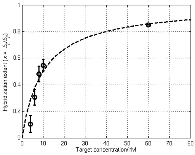
Results of a DNA target concentration series using the active CMOS biosensor array in which the hybridization extent x is plotted as a function of the solution target concentration. The dashed line shows the Langmuir fit to this equilibrium isotherm which yields a binding constant Ka of approximately 1×10⁸ M−1. Error bars for the four lowest target concentrations indicate the standard deviation from three separate experiments.
| (2) |
where CT is the solution target concentration which is assumed to be much larger than that needed to fully react with the probe layer. By fitting the data in Fig. 4 according to (2), Ka is found to be approximately 1×10⁸ M−1. This value of Ka falls in the range determined in previous studies involving surface-based assays (107 to 109 M−1) (Levicky and Horgan, 2005).
Although the smallest target coverage measured using our platform is about 1×1012 cm−2 (where x = 0.1 and the corresponding target concentration is 4 nM), as shown in Fig. 4, this is not the detection limit of the sensor. Rather, the hardware detection limit of the device is determined by the lowest measurable current. The hardware sensitivity limit can be evaluated from electronic measurement of the dynamic range of the sensor ADCs (when operated at a 10 kHz sampling rate). These measurements indicate that the smallest current that can be detected with a signal-to-noise ratio of three (Skoog et al., 1998) is 550 pA. This sets a detection limit of approximately 4×1010 cm−2 (or equivalently, a 50 pM target concentration given the calculated value of Ka above) assuming the maximum redox current Imax from the Fc reaction can be expressed using (Bard and Faulkner, 2001)
| (3) |
which applies to surface-bound electroactive species where n is the number of electrons transferred (one for the Fc reaction), F is the Faraday constant, R is the molar gas constant, T is the absolute temperature, and ν is the CV scan rate.
3.3. Real-time DNA detection
Observation of the entire hybridization process in real time has several advantages. First, the point at which equilibrium has been reached during hybridization can be determined unambiguously to improve assay reproducibility and sensitivity (Bhanot et al., 2003). Second, kinetic studies of DNA binding can be carried out to provide insight into the physical processes governing affinity-based sensing (Peterson et al., 2001). Lastly, the additional data provided by real-time sensing allows temporal averaging of the measured signal to be performed. This could improve signal-to-noise ratio by reducing the effect of independent noise sources, such as those arising from non-ideal instrumentation, as well as interfering biochemical processes like cross-hybridization, which become more noticeable in assays exhibiting low expression levels (Dai et al., 2002; Vikalo et al., 2006).
There are numerous approaches to real-time monitoring of surface bio-affinity reactions. For example, surface plasmon resonance (SPR) (Liedberg et al., 1983), quartz crystal microbalance (QCM) (Ward and Buttry, 1990), and cantilever (Fritz et al., 2000) sensors are similarly capable of performing real-time DNA sensing. However, electrochemical sensing techniques have the advantage of simple hardware compared to optical techniques and facile CMOS integration without surface micromachining or more complex post-processing as with cantilever (Hafizovic et al., 2004; Hierlemann et al., 2003) or QCM fabrication.
Fig. 5 demonstrates the measurement of real-time kinetics when 60 nM of T1 is hybridized to complementary P1. This CV measurement is taken at one of the 100 μm WEs, with a scan repeated every 5 min and the cell potential held at 0 V between scans. An increase in the area of the redox target peak is evident over time. The maximum extent of hybridization, reached after about 35 min, is about 6.8×1012 cm−2.
Fig. 5.
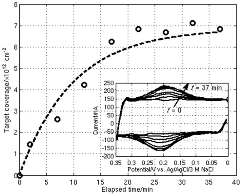
Real-time sensing of DNA probe-target hybridization at one 100 μm WE in which a CV scan is run every 5 min. The measured data is fit to a first-order rate equation (dashed line) following Langmuir kinetics. Inset shows the results from each CV scan over time.
Ignoring mass-transport limitations, effects of finite reaction volume, interactions among surface sites, and assuming that no probes have hybridized at time t = 0, the coverage of DNA duplexes on the WE surface as a function of time ST(t) can be expressed as (Dai et al., 2002)
| (4) |
The time constant τ over which the system reaches equilibrium is given by
| (5) |
where the forward rate constant kf and reverse rate constant kr are taken to be related by Ka = kf/kr. Performing a non-linear, least-squares fit of the real-time curve using (4) and (5) (also plotted in Fig. 5) gives a τ of about 590 s. From this, and using the value of Ka determined previously, kf and kr are calculated to be 2.4×10⁴ M−1 s−1 and 2.4×10⁻⁴ s−1, respectively. Although these results fall in the same order of magnitude as rate constants measured by others using QCM (Okahata et al., 1998) and surface plasmon fluorescence spectroscopy (Tawa et al., 2005) techniques, our measured value of Ka is relatively smaller, most likely because avidin-biotin spacers were used for probe immobilization in the referenced works.
3.4. Multiplexed and specific detection
We demonstrate multiplexed and specific detection using the CMOS biosensor array by functionalizing the chip with two distinct probes and then hybridizing each with its complementary target. Probes P1 and P2 are spotted on four different WEs each using a fluid microinjection system (IM-300, Narishige, East Meadow, NY, USA) capable of delivering nanolitre volumes of probe solution to the electrode surface.
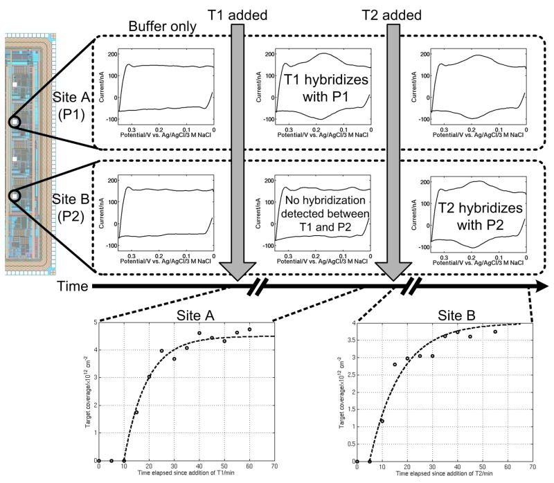
Initially, 6 nM of target T1 is introduced, and Fig. 6 shows the response at one of the 100 μm WEs functionalized with P1 (denoted “site A”) after 60 min. A distinct current peak can be seen, indicating that hybridization has occurred. The remaining WEs functionalized with P1 show similar behavior. Conversely, those WEs on which P2 is immobilized do not exhibit a hybridization signal, as P2 and T1 have little affinity for one another. The output from the sensor at one of the 100 μm WEs functionalized with P2 (denoted “site B”) is also displayed in Fig. 6.
Fig. 6.
Example of real-time, multiplexed and specific DNA detection using the active CMOS biosensor array. Site A is functionalized with probe P1 and site B with P2. Target T1 is added, followed by T2 at a later time. Hybridization is observed at site A, where P1 hybridizes with fully-complementary T1, while no hybridization is seen at site B. After T2 is added, hybridization is observed at site B while the signal at site A remains constant. The extent of hybridization at sites A and B as a function of time is also shown.
Next, 6 nM of target T2 is introduced. After 55 min, the hybridization signal at site B is evident, as shown in Fig 6. The signal at site A (measured at the same time) has not changed, however, since T1 is still present in solution. A separate experiment confirmed that sites functionalized with P1 do not exhibit any hybridization when T2 is added to the buffer first.
Fig. 6 also shows the measured target coverages at sites A and B in real time. The value of τ for the hybridization processes are approximately 540 s and 740 s at site A and B, respectively. The slight shift of the data relative to the origin is attributed to mass transport limitations at the early times of hybridization. These data demonstrate that our biosensor platform is capable of performing real-time monitoring of DNA hybridization in a multiplexed fashion.
4. Future work
Although the density of the current CMOS biosensor array is approximately 250 cm−2, this can be increased to over 6000 cm−2 for the same 100×100 μm2 WE area by optimizing the physical layout of the on-chip electronics. This density would be comparable to the commercial detection system in (Ghindilis et al., 2007) while incorporating the full potentiostat sensing electronics on chip.
Additional ongoing work involves the extension of our CMOS biosensor array for use in clinical gene expression samples that have traditionally been analyzed with fluorescence-based arrays. This will enable us to evaluate how the presence of a large excess of nonspecific DNA impacts the detection sensitivity of our platform.
5. Conclusions
Our active CMOS-integrated electrochemical biosensor array has the potential to enable portable DNA diagnostic platforms for point-of-care medical and biological applications. In addition, the use of ferrocene-conjugated DNA targets allows the detection of DNA hybridization in real time, a task not possible with traditional fluorescence-based assays. We believe that our approach to electrochemical biosensor implementation will provide a basis for future technological developments in high-throughput, portable DNA diagnostic platforms. Fully-integrated CMOS electrochemical biosensors could reduce the cost of nucleic-acid diagnostic platforms, leveraging the tremendous economies of scale associated with the semiconductor industry.
Supplementary Material
Acknowledgments
This work was supported in part by Grant Number HG003089 from the National Human Genome Research Institute, the Semiconductor Research Corporation (SRC) Center for Circuit and System Solutions (C2S2), the Catalyst Foundation, and an Intel Foundation Ph.D. Fellowship.
Footnotes
Publisher's Disclaimer: This is a PDF file of an unedited manuscript that has been accepted for publication. As a service to our customers we are providing this early version of the manuscript. The manuscript will undergo copyediting, typesetting, and review of the resulting proof before it is published in its final citable form. Please note that during the production process errors may be discovered which could affect the content, and all legal disclaimers that apply to the journal pertain.
References
- Bard AJ, Faulkner LR. Electrochemical Methods: Fundamentals and Applications. 2. Wiley; New York: 2001. [Google Scholar]
- Bhanot G, Louzoun Y, Zhu J, DeLisi C. Biophysical Journal. 2003;84(1):124–135. doi: 10.1016/S0006-3495(03)74837-1. [DOI] [PMC free article] [PubMed] [Google Scholar]
- Chahma M, Lee JS, Kraatz HB. Journal of Electroanalytical Chemistry. 2004;567(2):283–287. [Google Scholar]
- Dai H, Meyer M, Stepaniants S, Ziman M, Stoughton R. Nucleic Acids Research. 2002;30(16):e86. doi: 10.1093/nar/gnf085. [DOI] [PMC free article] [PubMed] [Google Scholar]
- Di Giusto DA, Wlassoff WA, Giesebrecht S, Gooding JJ, King GC. Angewandte Chemie International Edition. 2004;43(21):2809–2812. doi: 10.1002/anie.200352977. [DOI] [PubMed] [Google Scholar]
- Di Gleria K, Hill HAO, Wong LL. FEBS Letters. 1996;390(2):142–144. doi: 10.1016/0014-5793(96)00648-5. [DOI] [PubMed] [Google Scholar]
- Drummond TG, Hill MG, Barton JK. Nature Biotechnology. 2003;21(10):1192–1199. doi: 10.1038/nbt873. [DOI] [PubMed] [Google Scholar]
- Ekins RP, Chu FW. Clinical Chemistry. 1991;37(11):1955–1967. [PubMed] [Google Scholar]
- Fan C, Plaxco KW, Heeger AJ. Proceedings of the National Academy of Sciences USA. 2003;100(16):9134–9137. doi: 10.1073/pnas.1633515100. [DOI] [PMC free article] [PubMed] [Google Scholar]
- Fritz J, Baller MK, Lang HP, Rothuizen H, Vettiger P, Meyer E, Guntherodt HJ, Gerber C, Gimzewski JK. Science. 2000;288(5464):316–318. doi: 10.1126/science.288.5464.316. [DOI] [PubMed] [Google Scholar]
- Gemma N, O’uchi S, Funaki H, Okada J, Hongo S. IEEE International Solid-State Circuits Conference; 2006. pp. 560–561. [Google Scholar]
- Ghindilis AL, Smith MW, Schwarzkopf KR, Roth KM, Peyvan K, Munro SB, Lodes MJ, Stöver AG, Bernards K, Dill K, McShea A. Biosensors and Bioelectronics. 2007;22(9–10):1853–1860. doi: 10.1016/j.bios.2006.06.024. [DOI] [PubMed] [Google Scholar]
- Gong P, Levicky R. Proceedings of the National Academy of Sciences USA. 2008;105(14):5301–5306. doi: 10.1073/pnas.0709416105. [DOI] [PMC free article] [PubMed] [Google Scholar]
- Gooding JJ. Electroanalysis. 2002;14(17):1149–1156. [Google Scholar]
- Hafizovic S, Barrettino D, Volden T, Sedivy J, Kirstein KU, Brand O, Hierlemann A. Proceedings of the National Academy of Sciences USA. 2004;101(49):17011–17015. doi: 10.1073/pnas.0405725101. [DOI] [PMC free article] [PubMed] [Google Scholar]
- Herne TM, Tarlov MJ. Journal of the American Chemical Society. 1997;119(38):8916–8920. [Google Scholar]
- Hierlemann A, Brand O, Hagleitner C, Baltes H. Proceedings of the IEEE. 2003;91(6):839–863. [Google Scholar]
- Hofmann F, Frey A, Holzapfl B, Schienle M, Paulus C, Schindler-Bauer P, Kuhlmeier D, Krause J, Hintsche R, Nebling E, Albers J, Gumbrecht W, Plehnert K, Eckstein G, Thewes R. Electron Devices Meeting, 2002. IEDM ‘02. Digest International. 2002:488–491. [Google Scholar]
- Ihara T, Maruo Y, Takenaka S, Takagi M. Nucleic Acids Research. 1996;24(21):4273–4280. doi: 10.1093/nar/24.21.4273. [DOI] [PMC free article] [PubMed] [Google Scholar]
- Johns D, Martin K. Analog Integrated Circuit Design. Wiley; New York: 1997. [Google Scholar]
- Levicky R, Horgan A. Trends in Biotechnology. 2005;23(3):143–149. doi: 10.1016/j.tibtech.2005.01.004. [DOI] [PubMed] [Google Scholar]
- Levine PM, Gong P, Shepard KL, Levicky R. IEEE Custom Integrated Circuits Conference; 2007. pp. 825–828. [Google Scholar]
- Liedberg B, Nylander C, Lunström I. Sensors and Actuators. 1983;4:299–304. [Google Scholar]
- Lipshutz RJ, Morris D, Chee M, Hubbell E, Kozal MJ, Shah N, Shen N, Yang R, Fodor SPA. BioTechniques. 1995;19(3):442–447. [PubMed] [Google Scholar]
- Millan KM, Saraullo A, Mikkelsen SR. Analytical Chemistry. 1994;66(18):2943–2948. doi: 10.1021/ac00090a023. [DOI] [PubMed] [Google Scholar]
- Okahata Y, Kawase M, Niikura K, Ohtake F, Furusawa H, Ebara Y. Analytical Chemistry. 1998;70(7):1288–1296. doi: 10.1021/ac970584w. [DOI] [PubMed] [Google Scholar]
- Peterson AW, Heaton RJ, Georgiadis RM. Nucleic Acids Research. 2001;29(24):5163–5168. doi: 10.1093/nar/29.24.5163. [DOI] [PMC free article] [PubMed] [Google Scholar]
- Schena M. Microarray Analysis. Wiley; Hoboken: 2003. [Google Scholar]
- Schena M, Shalon D, Davis RW, Brown PO. Science. 1995;270(5235):467–470. doi: 10.1126/science.270.5235.467. [DOI] [PubMed] [Google Scholar]
- Schienle M, Paulus C, Frey A, Hofmann F, Holzapfl B, Schindler-Bauer P, Thewes R. IEEE Journal of Solid-State Circuits. 2004;39(12):2438–2445. [Google Scholar]
- Shen G, Tercero N, Gaspar MA, Varughese B, Shepard K, Levicky R. Journal of the American Chemical Society. 2006;128(26):8427–8433. doi: 10.1021/ja0571500. [DOI] [PMC free article] [PubMed] [Google Scholar]
- Skoog DA, Holler FJ, Nieman TA. Principles of Instrumental Analysis. 5. Saunders; Philadelphia: 1998. [Google Scholar]
- Steel AB, Herne TM, Tarlov MJ. Analytical Chemistry. 1998;70(22):4670–4677. doi: 10.1021/ac980037q. [DOI] [PubMed] [Google Scholar]
- Tawa K, Yao D, Knoll W. Biosensors and Bioelectronics. 2005;21(2):322–329. doi: 10.1016/j.bios.2004.10.024. [DOI] [PubMed] [Google Scholar]
- Ulman A. Chemical Reviews. 1996;96(4):1533–1554. doi: 10.1021/cr9502357. [DOI] [PubMed] [Google Scholar]
- Vig JR. Journal of Vacuum Science and Technology A. 1985;3(3):1027–1034. [Google Scholar]
- Vikalo H, Hassibi B, Hassibi A. IEEE Transactions on Signal Processing. 2006;54(6):2444–2455. [Google Scholar]
- Wang J. Analytica Chimica Acta. 2002;469:63–71. [Google Scholar]
- Ward MD, Buttry DA. Science. 1990;249(4972):1000–1007. doi: 10.1126/science.249.4972.1000. [DOI] [PubMed] [Google Scholar]
- Yu CJ, Wan Y, Yowanto H, Li J, Tao C, James MD, Tan CL, Blackburn GF, Meade TJ. Journal of the American Chemical Society. 2001;123(45):11155–11161. doi: 10.1021/ja010045f. [DOI] [PubMed] [Google Scholar]
Associated Data
This section collects any data citations, data availability statements, or supplementary materials included in this article.


