Abstract
We present a simple and efficient method to covalently immobilize graphene on silicon wafers using perfluorophenylazide (PFPA) as the coupling agent. Graphene sheets were covalently attached to PFPA-functionalized wafer surface by a simple heat treatment under ambient conditions. The formation of single and multiple layers of graphene were confirmed by Raman spectroscopy, and optical and atomic force microscopy. Evidence of covalent bond formation between graphene and PFPA decorated silicon wafer was given by X-ray photoelectron spectroscopy and sonication treatment.
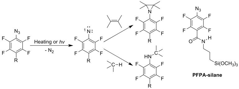
Graphene, a two-dimensional atomic thin layer of carbon nanostructure, has emerged as a unique nanoscale material with promising applications in electronics due to its stable crystal structure, optical transparency, and its exceptional electronic properties of high electron mobility and high saturation velocity for both electrons and holes1-7. However, realization of these potentials has been severely hampered by the availability of large-scale and stable graphene structures that are needed for electronic device fabrication. Furthermore, graphene films with well-defined and controllable surface and interface properties are important for both fundamental studies and practical applications of the material.8,9 Among various reported preparation methods,10-17 mechanical cleavage of highly oriented pyrolytic graphite (HOPG) remains to be the most popular and successful in producing single or few layers of graphene sheets.18 The earliest approach involves the use of a Scotch tape to peel multiple layers of graphene from HOPG, and transfer the sheets to a substrate by pressing followed by releasing. The films obtained in this manner contain different numbers of graphene layers, and the percentage of single graphene sheets varies from sample to sample. An improved version of the mechanical cleavage technique involves applying external pressure to press HOPG on the substrate and thus physically transferring the material from HOPG to the substrate.19,20 Chou and coworkers used the pillars on a stamp fabricated by nanoimprinting to cut and exfoliate graphene islands from HOPG, and then transferred the films from the stamp to the device active areas on a substrate.19 Padture et al. fabricated a graphite stamp by etching into HOPG using the technique of photolithography. The HOPG stamp was then pressed onto a silicon wafer creating arrays of multi-layered graphene sheets on the substrate surface.20 The graphene sheets deposited by these transferring methods are physisorbed on the substrate and can be easily removed by solvent wash (with isopropanol or acetone) or sonication.21 Here, we report a method to covalently attach graphene to silicon wafers using perfluorophenylazides (PFPA) as the coupling agent. Upon photochemical or thermal activation, the azido group gives the highly reactive singlet perfluorophenylnitrene that can subsequently undergo C-H insertion and/or C=C addition reactions with the neighboring molecules (Scheme 1).22,23 When the R group on PFPA contains a functional group that can be chemisorbed on the substrate, the PFPF serves as a heterobifunctional coupling agent attaching materials to the substrate surface via the insertion and/or addition reactions with the material. We have successfully employed functionalized PFPAs for the immobilization of polymers24 and small molecules25 to solid substrates. Graphene, having a network of sp2 C atoms, could in principle undergo addition reaction with nitrene to form the aziridine adduct (Scheme 1). In fact, PFPAs have been successfully used to functionalize C6026 and carbon nanotubes.27 To covalently immobilize graphene, we first treat the silicon wafer with a silane-functionalized PFPA (PFPA-silane, Scheme 1), introducing PFPA to the wafer surface. HOPG was then brought in contact with the PFPA-functionalized wafer, and was subsequently attached to the wafer surface upon activation of the PFPA moiety.
Scheme 1.
Thermally and photochemically initiated reactions of PFPA.
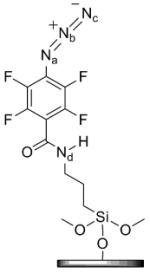
To test the feasibility of the approach, a simple experimental protocol was designed as shown in Scheme 2. Silicon wafers with an oxide layer of ~ 300 nm thick were cleaned with the Pirahna solution (7:3 v/v conc. H2SO4/35 wt % H2O2) followed by thorough washing with boiling water. The wafer was then treated with a solution of PFPA-silane in toluene (12.6 mM) for 4 h, washed with toluene, and cured at room temperature overnight. HOPG was placed on the PFPA-functionalized wafer, and was pressed by applying pressure on top of the HOPG (~10 psi). The assembly was brought to 140 °C and was subsequently heated for 40 min. The HOPG was then removed, and the resulting wafer was sonicated in isopropanol and N-methyl-2-pyrrolidone (NMP) for 10 min, respectively, washed with NMP followed by acetone, and dried with nitrogen.
Scheme 2.
Fabrication of covalently immobilized graphene on silicon wafer via the PFPA-silane coupling agent.
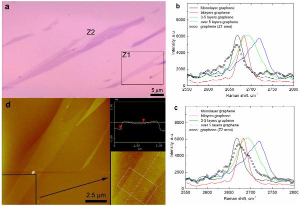
The immobilized graphene films were investigated by optical microscopy, atomic force microscopy, and Raman spectroscopy. Large pieces of graphene films were observed under the optical microscope, the size of stripes Z1 and Z2 being 2 × 15 μm2 and 4 × 50 μm2, respectively (Figure 1a). The films were further studied by Raman spectroscopy to determine the number of graphene layers of the obtained films.28,29 Reference samples were prepared by the conventional mechanical cleavage method using Scotch tape to transfer graphene sheets from HOPG to a clean wafer. The single-layer graphene showed the characteristic Raman 2D band at 2668 cm−1. Increases in the number of graphene layers result in peak shift gradually. Two (2) and three to five (3-5) layers of graphene peaked at 2682 cm−1 and 2692 cm−1, respectively, whereas greater than 5 layers of graphene and the bulk HOPG showed a broad absorption at 2720 cm−1 (Figure 1b and 1c, solid curves). By comparing the shape and peak position of our samples with those of the reference, the number of graphene layers on the covalently immobilized films can be determined. The Raman spectrum of the Z1 region (open-circle curve in Figure 1b) gave a peak at around 2668 cm−1 matching that of the single-layer graphene, confirming that the film contained only single-layer graphene sheets. In the Z2 region (Figure 1c, open circle curve), the Raman spectrum showed a strong single layer graphene peak at around 2668 cm−1 as well as a smaller shoulder at around 2700 cm−1, indicating that the film consists of a mixture of single and multiple layers of graphene sheets. AFM and sectional analysis of the Z1 region revealed the average height of the film to be 0.84 nm (Figure 1d), which is consistent with the thickness of a single graphene sheet. The reported value of the AFM step height of a single-layer graphene sheet on silicon wafer ranges from 0.4 to 1.0 nm.10,16,30 This result further confirmed that the film in the Z1 region was indeed single-layer graphene.
Figure 1.
a) Optical image of the covalently immobilized graphene films on silicon wafer; b), c) Raman spectra of the covalently immobilized graphene film in Z1 (b), and Z2 (c) region (open circle curves), and physisorbed graphene on wafer prepared by the Scotch tape method (solid curves), λlaser = 532 nm; d) AFM image of the Z1 region. Inset is the magnified image of the area indicated by the box and arrow in d), and the sectional analysis showing the thickness of the film to be 0.84 nm.
An advantage of covalently immobilized graphene film is its excellent stability. The graphene layers physisorbed on the substrate prepared by the Scotch tape method can be easily removed by solvent washing.21 The graphene films covalently immobilized by the PFPA coupling agent, however, remained on the wafer after both solvent washing and sonication. The samples prepared in this study were sonicated in isopropanol and NMP for 10 min, respectively. NMP is an excellent solvent for graphene.10 When a drop of NMP was placed on the graphene film prepared by the Scotch tape method, the film disappeared after the wafer was dried with N2. In fact, the Scotch-taped graphene can be readily removed by sonicating the samples in isopropanol or acetone. The fact that the covalently immobilized graphene films obtained with our method remained intact after repetitive solvent and sonication treatment clearly demonstrated that the bonding between graphene and the wafer is extremely strong and highly stable.
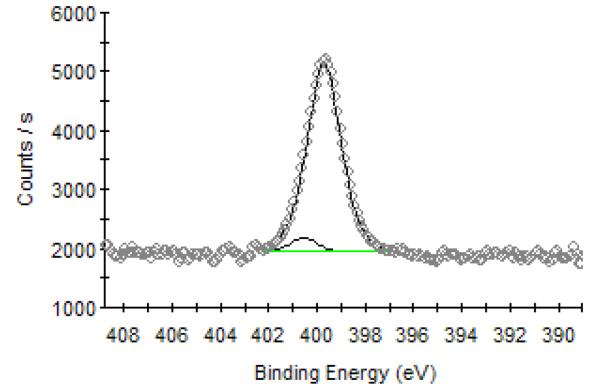
Further evidence on the covalent bond formation between graphene and PFPA-functionalized wafer was provided by X-ray photoelectron spectroscopy (XPS). Table 1 summarizes the XPS peak assignments of the N 1s core level spectrum of the PFPA moiety on the PFPA-functionalized wafer.25 After the graphene film was immobilized, the peak at 404.3 eV, which is originated from Nb of the N3 group (−Na=Nb+=Nc−), disappeared (Figure 2). This is consistent with the PFPA reaction where the N3 decomposes and splits off N2 after activation (Scheme 1). Simultaneously, Nc should also disappear resulting a significant decrease in the peak intensity at ~399.3 eV. However, a substantial increase in the peak intensity at 399.7 eV was observed in the XPS spectrum of the graphene sample (Figure 2). We attribute this to the N of the aziridine structure formed upon reaction of perflurophenylnitrene with graphene (Scheme 1). Similar XPS analysis was reported by Hirsch and coworkers where nitrene was allowed to react with carbon nanotubes (CNTs).31 A drastic increase in the peak intensity at 400.3 eV was observed and was attributed to the arizidine N formed between nitrene and CNT. The covalent bond formation between azide and graphene is furthermore supported by a very recent report by Kim et al. where the authors chemically modified epitaxial graphene with azidotrimethylsilane.32 Using high-resolution photoemission spectroscopy, the authors confirmed that covalent bonds indeed formed between the thermally generated nitrene and the epitaxial graphene.
Table 1.
XPS peak assignments of the N 1s core level spectrum of the PFPA moiety on PFPA-functionalized wafer.
 |
Binding Energy, eV a |
|||
| Na | Nb | Nc | Nd | |
| 401.4 | 404.3 | 399.3 | 400.8 | |
Data from reference 25.
Figure 2.
High-resolution XPS N 1s core level spectrum (open circle curve) and curve fitting (solid curves) of graphene film covalently immobilized on the PFPA-functionalized silicon wafer.
In summary, we have fabricated covalently immobilized graphene films on silicon wafers using PFPA-silane as the coupling agent. The process involves pressing HOPG on PFPA-functionalized wafer surface followed by thermal treatment initiating the covalent bond formation of the perfluorophenylnitrene with graphene. The nitrene formation can also be triggered photochemically, and we have obtained covalently immobilized graphene films by UV irradiation. In addition, this method can be readily applied to other substrates simply by changing the functional group on the PFPA. For example, by using a thiol-functionalized PFPA, we were able to covalently attach graphene sheets on gold films. This provides a facile approach to the construction of graphene-based integrated circuits on a wide range of substrates. The bonding molecular layer is expected to affect the electronic coupling of graphene with the substrate. Preliminary electrical measurement on a wide strip of immobilized graphene gave an I-V curve indicating that the chemically bonded graphene was conductive. In addition, the resistance measurement showed that the chemically bonded graphene film was slightly more resistive than the physically deposited film. We have developed a systematic approach to control the surface density, topography, and interface properties of the immobilized layer.33 The method developed here thus offers immense opportunities to investigate how surface and interface chemistry affect the electronic properties and performance of graphene-based electronic devices. Work in this aspect is currently underway.
Acknowledgements
This work was supported by Oregon Nanoscience and Microtechnologies Institute (ONAMI) and ONR under the contract N00014-08-1-1237, and NIH (2R15GM066279). We thank Professor Raj Solanki and Mr. Gopichand Nandamuri at the Department of Physics for their help in Raman spectroscopy and electrical measurements.
Reference
- 1.Geim AK, Novoselov KS. Nat. Mater. 2007;6:183–191. doi: 10.1038/nmat1849. [DOI] [PubMed] [Google Scholar]
- 2.Schedin F, Geim AK, Morozov SV, Hill EW, Blake P, Katsnelson MI, Novoselov KS. Nat. Mater. 2007;6:652–655. doi: 10.1038/nmat1967. [DOI] [PubMed] [Google Scholar]
- 3.Gilje S, Han S, Wang M, Wang KL, Kaner RB. Nano Lett. 2007;7:3394–3398. doi: 10.1021/nl0717715. [DOI] [PubMed] [Google Scholar]
- 4.Han MY, Ozyilmaz B, Zhang YB, Kim P. Phys. Rev. Lett. 2007;98:206805. doi: 10.1103/PhysRevLett.98.206805. [DOI] [PubMed] [Google Scholar]
- 5.Obradovic B, Kotlyar R, Heinz F, Matagne P, Rakshit T, Giles MD, Stettler MA, Nikonov DE. Appl. Phys. Lett. 2006;88:142102. [Google Scholar]
- 6.Tang YB, Lee CS, Chen ZH, Yuan GD, Kang ZH, Luo LB, Song HS, Liu Y, He ZB, Zhang WJ, Elello I, Lee ST. Nano Lett. 2009;9:1374–1377. doi: 10.1021/nl803025e. [DOI] [PubMed] [Google Scholar]
- 7.Chen JH, Ishigami M, Jang C, Hines DR, Fuhrer MS, Williams ED. Adv. Mater. 2007;19:3623–3627. [Google Scholar]
- 8.Eda G, Fanchini G, Chhowalla M. Nat. Nanotech. 2008;3:270–274. doi: 10.1038/nnano.2008.83. [DOI] [PubMed] [Google Scholar]
- 9.Park S, Ruoff RS. Nat Nanotech. 2009;4:217–224. doi: 10.1038/nnano.2009.58. [DOI] [PubMed] [Google Scholar]
- 10.Hernandez Y, Nicolosi V, Lotya M, Blighe FM, Sun ZY, De S, McGovern IT, Holland B, Byrne M, Gun'ko YK, Boland JJ, Niraj P, Duesberg G, Krishnamurthy S, Goodhue R, Hutchison J, Scardaci V, Ferrari AC, Coleman JN. Nat. Nanotech. 2008;3:563–568. doi: 10.1038/nnano.2008.215. [DOI] [PubMed] [Google Scholar]
- 11.Valles C, Drummond C, Saadaoui H, Furtado CA, He M, Roubeau O, Ortolani L, Monthioux M, Penicaud A. J. Am. Chem. Soc. 2008;130:15802–15804. doi: 10.1021/ja808001a. [DOI] [PubMed] [Google Scholar]
- 12.Berger C, Song ZM, Li XB, Wu XS, Brown N, Naud C, Mayou D, Li TB, Hass J, Marchenkov AN, Conrad EH, First PN, de Heer WA. Science. 2006;312:1191–1196. doi: 10.1126/science.1125925. [DOI] [PubMed] [Google Scholar]
- 13.Stankovich S, Dikin DA, Dommett GHB, Kohlhaas KM, Zimney EJ, Stach EA, Piner RD, Nguyen ST, Ruoff RS. Nature. 2006;442:282–286. doi: 10.1038/nature04969. [DOI] [PubMed] [Google Scholar]
- 14.Wu JS, Pisula W, Mullen K. Chem. Rev. 2007;107(3):718–747. doi: 10.1021/cr068010r. [DOI] [PubMed] [Google Scholar]
- 15.Sutter PW, Flege JI, Sutter EA. Nat. Mater. 2008;7:406–411. doi: 10.1038/nmat2166. [DOI] [PubMed] [Google Scholar]
- 16.Li XL, Wang XR, Zhang L, Lee SW, Dai HJ. Science. 2008;319:1229–1232. doi: 10.1126/science.1150878. [DOI] [PubMed] [Google Scholar]
- 17.Dato A, Radmilovic V, Lee ZH, Phillips J, Frenklach M. Nano Lett. 2008;8:2012–2016. doi: 10.1021/nl8011566. [DOI] [PubMed] [Google Scholar]
- 18.Novoselov KS, Geim AK, Morozov SV, Jiang D, Zhang Y, Dubonos SV, Grigorieva IV, Firsov AA. Science. 2004;306:666–669. doi: 10.1126/science.1102896. [DOI] [PubMed] [Google Scholar]
- 19.Liang X, Fu Z, Chou SY. Nano Lett. 2007;7:3840–3844. [Google Scholar]
- 20.Li DS, Windl W, Padture NP. Adv. Mater. 2009;21:1243–1246. [Google Scholar]
- 21.Meyer JC, Girit CO, Crommie MF, Zettl A. Appl. Phys. Lett. 2008;92:123110. [Google Scholar]
- 22.Poe R, Schnapp K, Young MJT, Grayzar J, Platz MS. J. Am. Chem. Soc. 1992;114:5054–5067. [Google Scholar]
- 23.Brunner J. Annu. Rev. Biochem. 1993;62:483–514. doi: 10.1146/annurev.bi.62.070193.002411. [DOI] [PubMed] [Google Scholar]
- 24.Yan MD, Ren J. Chem. Mater. 2004;16:1627–1632. [Google Scholar]
- 25.Al-Bataineh SA, Luginbuehl R, Textor M, Yan M. Langmuir. 2009;25:7432–7437. doi: 10.1021/la900334w. [DOI] [PMC free article] [PubMed] [Google Scholar]
- 26.Yan MD, Cai SX, Keana JFW. J. Org. Chem. 1994;59:5951–5954. [Google Scholar]
- 27.Pastine SJ, Okawa D, Kessler B, Rolandi M, Llorente M, Zettl A, Frechet JMJ. J. Am. Chem. Soc. 2008;130:4238–4239. doi: 10.1021/ja8003446. [DOI] [PubMed] [Google Scholar]
- 28.Ferrari AC, Meyer JC, Scardaci V, Casiraghi C, Lazzeri M, Mauri F, Piscanec S, Jiang D, Novoselov KS, Roth S, Geim AK. Phys. Rev. Lett. 2006;97:187401. doi: 10.1103/PhysRevLett.97.187401. [DOI] [PubMed] [Google Scholar]
- 29.Graf D, Molitor F, Ensslin K, Stampfer C, Jungen A, Hierold C, Wirtz L. Nano Lett. 2007;7:238–242. doi: 10.1021/nl061702a. [DOI] [PubMed] [Google Scholar]
- 30.Tung VC, Allen MJ, Yang Y, Kaner RB. Nat. Nanotech. 2009;4:25–29. doi: 10.1038/nnano.2008.329. [DOI] [PubMed] [Google Scholar]
- 31.Holzinger M, Abraha J, Whelan P, Graupner R, Ley L, Hennrich F, Kappes M, Hirsch A. J. Am. Chem. Soc. 2003;125:8566–8580. doi: 10.1021/ja029931w. [DOI] [PubMed] [Google Scholar]
- 32.Choi J, Kim K.-j., Kim B, Lee H, Kim S. J. Phy. Chem. C. 2009;113:9433–9435. [Google Scholar]
- 33.Liu L, Engelhard MH, Yan MD. J. Am. Chem. Soc. 2006;128:14067–14072. doi: 10.1021/ja062802l. [DOI] [PMC free article] [PubMed] [Google Scholar]


