Abstract
Many fabrication technologies have been used to build nano/mesoporous materials/filters with a good size control, but the integration of these systems into a microsystem format has been a challenge. Microfabricated nanofilters suffer from small open volume and low throughput. In this paper, we developed a novel fabrication strategy for massively-parallel, regular vertical nanochannel membranes with a uniform, well-controlled gap size of ~50 nm and a depth up to ~40 μm, by using only standard semiconductor fabrication techniques. The vertical nanofilter membranes were fabricated into an anisotropic nanofilter array, which demonstrates the ability to integrate nanofilters and micron-sized channels/pores seamlessly. We demonstrated efficient continuous-flow separation of large DNAs and small molecules in a two-dimensional vertical nanochannel array device. These ultrahigh-aspect-ratio nanochannels have the advantage of large open volume, enabling for high-throughput applications.
Introduction
Reliable fabrication of microporous/mesoporous structures has long been the focus of materials science, spurred by important applications such as molecular separation and filtration. Various techniques, such as nuclear track-etched membranes,1 colloidal micro/nanobead packing,2–4 polymer monolith,5, 6 anisotropic wet etching techniques,7 have already been well-established for generating the isotropic nanoporous/mesoporous materials with a good pore size control for various applications. However, applications of these materials to integrated molecular processing microsystems are often limited, mainly because of material imperfection and defects, limited structural rigidity, and other difficulties in system integration. More recently, interests have been increasing on the fabrication of anisotropic filters8 and/or bi-continuous materials,9 since their unique structures can lead to advanced functionality which cannot be obtained from materials with uniform, isotropic, randomly oriented pores.
In contrast, microfabrication of nanofilters and nanopores7–15 generally allows much better control on structural parameters and geometries. Regular-sized nanopores and nanochannels can be precisely machined using e-beam or photolithography and etching processes, which are compatible with other general clean room process and allow straightforward microsystem integration that combines different functions. While small-scale microfabrication of these systems is relatively expensive, scaling up to large-volume manufacturing of these systems is rather straightforward and indeed well-established. The materials typically used in these systems (silicon or glass) demonstrate much better structural reliability, which allows one to handle high mechanical force.10 Due to these reasons, these artificial nanofilters and nanochannels are being used for various applications such as biomolecule separation/sorting5, 16, 17 as well as drug delivery.11 One critical bottleneck of microfabricated artificial filters/pores, however, is that these nanochannels generally exhibit smaller open pore volume (sample processing volume), and as a result, lower sample throughput, compared with more traditional membrane materials such as gels. An ideal artificial membrane structure would have a high sample volume throughput, and would be possible to couple nanofilters/nanopores with other microchannels/micropores in an arbitrary way, in order to create advanced filter systems.
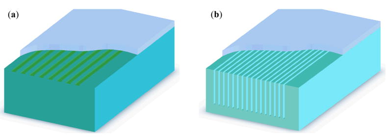
In this paper, we report a robust top-down fabrication technique of producing massively-parallel, regular nanochannels with good control of pore size for high-throughput membrane applications. Our approach is building high-aspect-ratio (ratio of depth to width) vertical nanochannels with a well-defined lateral width down to ~50 nm. Figure 1 shows the conceptual comparison of these planar nanochannels and vertical nanochannels. The cross-sectional flow area (open pore volume per unit length) of the vertical channels could be more than hundreds of times higher than the cross-sectional area of the planar channels. Therefore, the sample throughput (volume flow rate) of the vertical system could be a few orders of magnitude higher than the throughput of the planar system with a similar flow velocity, while they possess similar device characteristics due to the same critical dimension. Anisotropic etching of (110) silicon provides an attractive and effective method for fabrication of high-aspect-ratio structures with smooth and vertical sidewalls because of the high selectivity between (110) and (111) planes (larger than 100:1). As early as in 1975, Kendall used KOH etching to generate very narrow (0.6 μm wide), deep (~44 μm) trenches on Si wafers.12 However, expensive and time-consuming e-beam lithography was needed to pattern narrow channels for etching. Here, we develop this inexpensive method further to fabricate ultrahigh-aspect-ratio nanochannels with standard semiconductor microfabrication techniques.
Figure 1.
Cartoon illustrates the comparison of planar (low-aspect-ratio) nanochannel system (a) and (high-aspect-ratio) vertical nanochannel system (b). They both have the same critical dimension (depth for planar channels and width for vertical channels) but the open volume of vertical channels can be more than ten times or even a hundred times larger than planar channels.
Experimental
Fabrication of high-aspect-ratio vertical nanochannels
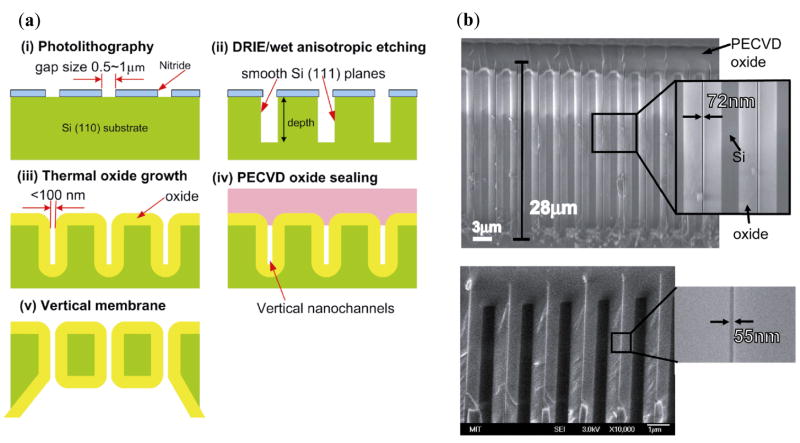
The overall fabrication process for creating massively parallel, vertical nanochannels is outlined in Figure 2a. Commercial p-type Czochralski grown 6″ (110) wafers with a resistivity of 10–20 Ω cm and a thickness of 625 μm were used (El-CAT, Inc., NJ). First, a thin layer of low-stress low-pressure chemical vapor deposition (LPCVD) silicon nitride was deposited on (110) silicon substrate to provide an etch mask for KOH etching. Then channel patterns were defined by standard photolithography and etched to form narrow, deep trenches by anisotropic KOH etching. The features in this step were aligned to the (111) planes of silicon within 0.1 degree using the fan-shaped and diamond-shaped alignment mark.13, 14 the etch rate of (110) plane in 44 wt% KOH is around 75 nm min−1 at room temperature without stirring. Alternatively, deep reactive ion etching (DRIE) technique was also used to achieve deep trench etch with Bosch process, but a decent period of KOH etching should be followed to smooth the rough sidewall scallops resulted from DRIE process. After KOH etching, the sidewalls will end up with smooth, vertical (111) planes, which is important for ensuring nanochannel uniformity in the downstream oxidation process. It is well known that thermal oxidation process on Si results in a volume expansion of about a factor of 2.3, which could be used for reducing the trench widths in a highly controlled manner. After removal of the silicon nitride layer, scanning electron microscopy (SEM) was used to measure the gap size (trench width) in order to determine the oxide thickness. Based on the gap size, an oxide layer with appropriate thickness was grown to narrow the gap down to below 100 nm or even 10 nm. Finally, non-conformal PECVD (plasma-enhanced chemical vapor deposition) oxide deposition was performed to seal the trenches and form vertical nanochannels. Alternatively, the backside of the wafer can be etched to make a thin, vertical membrane across the Si wafer, if such geometry is preferred. Using this method, one could fabricate a large area of membranes with regular pores if needed. This fabrication process is inexpensive, and simple without any nanolithography and other special tools, and can be well controlled. In addition, this method allows much flexibility and easy system integration, and is straightforward to create massively-parallel nanochannels for large-scale membrane applications.
Figure 2.
(a) Schematic diagram of fabricating vertical nanochannels. (i) photolithography defines pattern structures; (ii) vertical trenches with smooth sidewalls are etched by either DRIE or anisotropic wet etching (KOH); (iii) thermal oxide growth further decreases the gap size; (iv) uniform PECVD oxide is deposited to seal narrow trenches; (v) backside etching of Si wafer yields thin membranes over a wide area (~6 inch wafers). (b) Cross-sectional SEM micrographs of slot-like vertical nanochannels with a uniform gap size of 72 nm and 55 nm. The channels are etched by KOH etching and have a depth of 28 μm. The channels are completely sealed by depositing 3 μm thick PECVD oxide.
Results and Discussion
Characterization of fabrication process
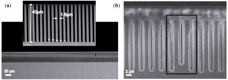
We have been able to fabricate 28 μm deep, slot-like trench arrays with a uniform gap size (lateral trench width) as narrow as 72 nm, even down to 55 nm throughout the depth of the trench, as shown in Figure 2b. The aspect ratio (depth-to-width ratio) of vertical nanochannels can be as high as 400. Compared to fabrication of high-aspect-ratio sub-micrometer channels with DIRE process reported by Mogensen et al.,15 our strategy allows to produce nanostructures with much higher aspect ratio and a smaller, more uniform nanofilter gap by minimizing the sidewall roughness during the vertical etching process. In this technique, KOH etching was performed at room temperature in contrast to more conventional etching temperature (>70°C). We have found out that etching at high temperature tends to form trenches of non-uniform depth with the same widths, as shown in Figure 3(b). This non-uniformity in depth causes a serious problem of non-uniform gap sizes after thermal oxidation, caused by uneven expansion and distortion of oxide film. However, KOH etching at room temperature can produce highly uniform channel depths, as shown in Figure 3(a). The major cause for such non-uniformity might be gas bubbles generated on the silicon surface during the etching process. When bubbles get trapped and remain in a narrow trench, the etch rate in that particular region would decrease.16 High temperature etching generates a much larger quantity of bubbles (due to higher etch rates) than low temperature process. With low temperature etching, we were able to produce 120 μm deep trenches uniformly (data not shown in this paper). The maximum attainable depth is still under investigation.
Figure 3.
(a) Cross-sectional SEM image of 40 μm deep trenches produced by KOH etching at room temperature. The uniform trench depth has been achieved. (b) Cross-sectional SEM image showing the non-uniform gap size after oxidation. The designated trench is shallower than the neighbor ones as a result of KOH etching at high temperature (70 °C). The structural asymmetry causes distortion due to an inequality of stress acting on two channel walls in thermal oxidation process.
Another important issue is the control of the gap size. In this technique, the gap size is controlled by growing the approximate thickness of thermal oxide. Although the one-dimensional (1D) thermal oxidation of silicon is described by the well-known Deal-Grove model and can be controlled very well, the oxidation of two-dimensional (2D) or three-dimensional (3D) structures, such as slots and pillars, is more complicated and the rate is pattern-dependent.17 We have found out that the oxide of the top surface of silicon pillars is around 50 nm thicker than the oxide on planar surface with a nominal (planar) oxide of 500 nm grown. This step height will cause a significant problem in traditional bonding such as anodic bonding. We believe that this pattern-dependent oxidation is due to the complex thermal stress during oxidation process. We also observed the non-uniform gap size of a channel when it is shallower than its neighboring channels, as shown in Figure 3(b). The structures seem to be distorted and bended, resulting in a larger gap size. We think this structural asymmetry results in an inequality of stress in these two walls during thermal oxidation and the distortion of the structure. Therefore, it is important to produce channels with uniform depths in order to achieve a uniform gap size. Overall, based on theoretical prediction (1 D model of oxidation) and experimental characterization data, we were able to control the final gap size of nanochannels down to ~50 nm within 10% of our intended target gap size. Precise control of the gap size might require careful 2D or 3D modeling of oxidation process. The ultimate minimum gap size attainable using this technique remains to be investigated. It was previously reported that the oxidation rate within the trench could be retarded due to hindered transport of oxidizing species.18 In such cases, the gap size might become non-uniform in very narrow, deep trenches due to this effect. However, if the species can transport to the nanochannels from the side besides from the top entrance (as in Figure 6), the limitation can be pushed further.
Figure 6.
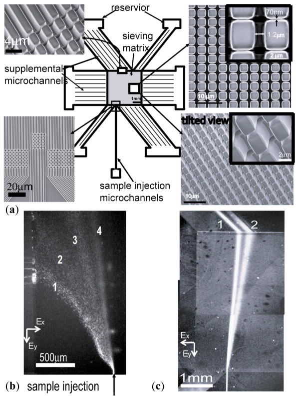
Continuous fractionation of biomolecules through the two-dimensional anisotropic pillar array device. (a) The device includes a sieving matrix and surrounding microfluidic channels. The pillar array consists of horizontal nanochannels with a width of 70 nm and longitudinal microchannels with a width of 1.2 μm. Supplemental microchannels connecting sieving matrix and reservoirs are 1.5 μm in width. They are all 15 μm deep. (b) Fluorescence micrographs show separation of the mixture of λ-DNA Hind III digest. Electric fields Ex and Ey applied both in horizontal and longitudinal directions in the sieving matrix are 80 V cm−1 and 30 V cm−1, respectively. Band assignment: (1) 23.13 kbp; (2) 9.4 kbp; (3) 6.58 kbp; (4) 4.36 kbp. (c) Fluorescence micrographs showing separation of the mixture of FITC (2) and R-phycoerythrin (1). The nanofilter size is ~40 nm. Ex=250 V cm−1 and Ey=40 V cm−1. It is obtained by combining two fluorescence micrographs taken in the same run but with two different filter sets since they have a different spectrum.
Nanochannels are sealed to make enclosed channels by a non-conformal oxide deposition from the top. This oxide deposition step serves three purposes. Firstly, it is to seal trenches and to form micro/nanochannels. The non-conformal PECVD oxide deposition is chosen because of its high deposition rate, enabling one to deposit a thick (~10 μm) film. As shown in Figure 2b, trenches can be completely sealed by 3 μm thick PECVD oxide without defects. We have found that trenches with widths less than 1.5 μm can be easily sealed by a 3~5 μm thick PECVD oxide (data not shown here). Another benefit of PECVD process is that almost no deposition takes place in the sidewalls so that the uniform gap size of vertical nanochannels will not be affected by the deposition process. Secondly, PECVD oxide sealing is able to eliminate the rounded shape emerging from oxidation process and keeps the gap size uniform along the trenches (Fig. 2(b)). Finally, trench-filling eliminates the need for substrate bonding process, which tends to become very challenging or even unfeasible especially with a thick oxide film on the surface. In fact, as we mentioned before, the thermal oxidation of high-aspect-ratio silicon trench arrays causes a step height between the regions with different patterns and then traditional bonding methods such as anodic bonding and fusion bonding would fail.
Modified approach for fabricating embedded vertical nanochannels
This trench filling method with PECVD oxide deposition is applied to the situation where all of the structural dimensions are small, usually less than 2 μm. In many applications, however, nanochannels need to be connected with microchannels (dimensions larger than 10 μm) to realize novel functions such as preconcentration.19 A modified approach has been developed to overcome this limitation by producing embedded nanochannels. The fabrication process is shown in Figure 4a. After KOH etching of deep trenches, PECVD oxide and LPCVD polysilicon were sequentially deposited on the trenches. Then, the thermal oxide was grown to narrow the gap size down to the desired value. Figure 4b clearly shows that PECVD oxide deposition at 400 °C is rather non-conformal process while successive LPCVD polysilicon deposition at 620 °C and the pressure of 250 miliTorr occurs uniformly on the sidewalls and seals the trenches completely. The combination of these non-conformal and conformal processes allows us to maintain a uniform gap size along the trench, except very near the trench entrance, after deposition.
Figure 4.
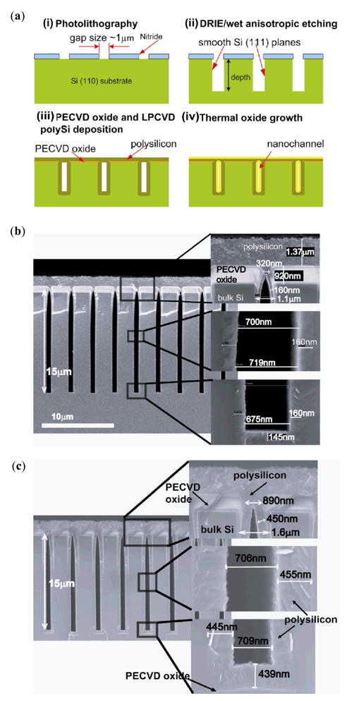
Modified approach for fabricating embedded vertical nanochannels. (a) Schematic diagram of fabrication process. (i) patterning channels by standard photolithography; (ii) etching by either DRIE or anisotropic wet etching (KOH); (iii) depositing PECVD oxide and conformal LPCVD polysilicon to seal trenches sequentially; (iv) growing thermal oxide to decreases the gap size. (b,c) Cross-sectional SEM images of 15 μm deep trenches deposited with 900 nm thick PECVD oxide and 1.37 μm thick LPCVD polysilicon sequentially. The gap size uniformly changes from 1.6 μm to 706 nm (b) and from 1.1 μm to 700 nm (c) after deposition. It shows that their final gap after LPCVD polysilicon deposition becomes almost the same although their initial gap size differs by 0.5 μm.
In fact, we have found out that the single LPCVD deposition of polysilicon or LTO oxide without the preceding PECVD deposition step caused non-uniform step coverage in the trenches (data not shown here). Although LPCVD process is believed to be much more conformal than PECVD process, its capability of conformally depositing uniform materials in high-aspect-ratio trenches is impaired. Tuning the appropriate parameters of LPCVD process such as temperature and pressure could achieve better step coverage, but these parameters will vary for the trenches with different aspect ratios. Our method provides an alternative way to realize conformal LPCVD deposition in high-aspect-ratio trenches by controlling the profile of trench openings with PECVD deposition. Recently, atomic layer deposition (ALD) has become an attractive technique for depositing thin films in semiconductor industry because it offers the advantages of pinhole-free, large area uniformity, and excellent conformality20. ALD might have the capability of achieving deposition as uniform and conformal as thermal oxidation but could be more time-consuming and expensive, with a limited materials choice readily available. We do not have access of ALD to test it yet.
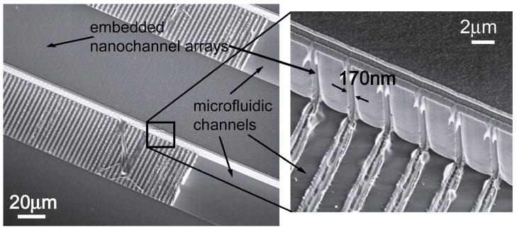
Interestingly, the final gap size becomes almost the same although they differ by 0.5 μm before deposition as shown by comparison of the case (b) and (c) in Figure 4. It turns out that the final gap size after deposition doesn’t depend on the initial gap size, but is the difference between the initial gap size and the trench opening after the PECVD oxide deposition, which is determined by PECVD process. When the initial gap sizes of two channels differ slightly (less than 1 μm, for instance), their film profiles of oxide by PECVD deposition are very much identical, resulting in the same final gap sizes. Therefore, it is very straightforward to control the final gap size by tuning PECVD oxide deposition time as well as oxidation time. This is a very important result because it can cancel out some defects of large gaps due to photolithography or etching process to some degree. Also, this strong capping layer can prevent structures from bending or distorting during thermal oxidation process, as described above. We believe that this approach will allow us to generate robust high-aspect-ratio embedded vertical nanochannels with precise control on structural parameters, although further investigation on the limitation of this approach is needed. For one application, using this technique, we fabricated a high-throughput nanofluidic preconcentrator, which consists of two parallel microchannels bridged by an embedded nanochannel array, as shown in Figure 5.
Figure 5.
Tilted-view SEM images of a high-throughput sample preconcentration device. It consists of two parallel 50-μm-wide channels, bridged by an embedded nanochannel array. The gap size of a nanochannel is 170 nm. All the channels have the same depth of 12 μm. The microchannels and nanochannels are etched by DRIE and KOH etching, respectively.
Continuous separation in a 2D anisotropic nanofilter array device
Micromachined regular sieving structures have attracted great interests as potential replacement with nanoporous gels for biomolecule separation. Recently, Fu and his coworkers21 reported a microfabricated planar anisotropic nanofilter array (ANA) for efficient, continuous-flow separation of DNA and proteins. However, these planar-nanochannel-based systems have the drawback of low sample throughput ~ 1 nL hour−1. Here, we develop a two-dimensional anisotropic vertical nanofilter array for high throughput biomolecule separation by using the fabrication techniques described above. The device consists of a two-dimensional periodic pillar array as the sieving structure, produced by etching horizontal channels and longitudinal channels sequentially (Fig 6(a)). In contrast to the depth of the shallow channels in the system of planar nanofilters by Fu21, the critical dimension of this device is the gap size (width) of the narrow (horizontal) channels, which is 70 nm. The gap size of the wide (longitudinal) channels is around 1.2 μm. The supplemental microfluidic channels connect the pillar arrays to the fluid reservoirs and also act as electric-current injectors to provide uniform electric fields Ex and Ey along two orthogonal directions over the sieving matrix22. The horizontal channels were etched by KOH etching while the longitudinal channels and other microchannels were etched by DRIE etching to the same depth. After thermal oxidation, all the channels were sealed by PECVD oxide deposition. Access holes were created by opening up the PECVD oxide film from the top. The nanofilter array device was filled with Tris-Borate-EDTA (TBE) 5× buffer during experiment. The λ-DNA Hind digest (New England Biolabs) was stained with the intercalating fluorescence dye YOYO-1 (Invitrogen) at a dye-to-base pair ratio of ~1:10 in 5× TBE buffer. The final DNA concentration was 40 μg mL−1.
As shown in Figure 6(b), the λ-DNA Hind III digest was continuously separated into four distinct streams in a few minutes with decent electric fields applied in two orthogonal directions. The shortest two fragments (2,322 bp and 2,027 bp) were missing, which is most likely due to their low concentration and weak signal. Further observation reveals that longer molecules deflected more from the injection (longitudinal) direction than small ones, suggesting longer ones have a higher jump passage rate through a nanofilter. This observation can be explained by the entropic trapping mechanism, consistent with the results of separating long DNAs in planar ANA.21, 23 In fact, the radii of gyration of these DNA fragments range from ~140 nm to 520 nm, which are all greater than the nanofilter gap size of 70 nm. Therefore, DNA crossing of nanofilter requires deformation of molecules and hernia formation at the cost of internal conformational entropy. Longer molecules have a larger surface area in contact with the nanofilter area and thus have a higher probability of forming the hernia that initiates the escape process. The line curvature of the DNA molecules is due to the slight nonuniformity of the electric fields over the sieving matrix.
With a smaller filter size of ~ 40 nm, we demonstrated the Ogston sieving in the vertical ANA. As shown in Figure 6(c), R-phycoerythrin (MW~240 kDa) and fluorescein isothiocyanate (FITC) (MW~389 Da) were clearly separated into two streams in TBE 10× buffer. The stream of FITC had a higher deflection angle than R-phycoerythrin, showing smaller molecules have a greater jump passage rate. Our observation suggests that the molecular sieving in vertical ANA be very similar to the relevant phenomena in planar ANA. Compared to the planar ANA and other continuous-flow systems,24 the important feature of our device is much higher sample processing rate of ~ 1 μL hour−1, and further improvement of throughput can be achieved simply by upscaling the channel depths. DNA prism was reported to achieve comparable throughput, but remains challenging for protein separation.22 For traditional gel-based separation technologies, typically ~10 μL samples can be processed in a batch mode (one elution separation after another), each requiring 30~60 mins typically. Therefore, the achieved throughput of our device would still be somewhat less than that of the current gel techniques. However, we would like to point out that such throughput in gel is achieved simply because the gels are in ~10 mm in thickness and ~10 cm in size, while our device is much smaller. Parallelization of our device on a wafer scale would definitely bring about higher throughput, if such high-throughput is deemed necessary. Although more efforts need to be made in optimizing the device and extending its utilization for separation of native proteins, its potential for an effective, high-throughput biomolecule separation has been demonstrated. We believe that this device could be a key to the efficient proteomic sample-preparation microsystems as well as purifying and separating various bioparticles and nanoparticles.
Conclusions
We have developed novel strategies for fabricating massively-parallel, high-aspect-ratio nanochannels by a combination of anisotropic etching and thermal oxidation. Nanochannels are sealed by CVD deposition, which eliminates the need for substrate bonding. Vertical nanochannels with a uniform gap size of 55 nm and aspect ratio as high as 400 have been demonstrated. Our fabrication processes are completely CMOS-compatible, without any nanolithography or non-conventional fabrication tools required. Gap sizes can be well controlled, and connection between nanochannels and microchannels can be made in a seamless way. This would pave the way for widespread application of solid-state, regular nanofilters in various membrane/filtration/separation applications, without suffering from the volume throughput limitation. We demonstrated a two-dimensional, anisotropic nanofilter array (ANA) device for efficient, continuous-flow, and high-throughput separation of biomolecules in minutes. The unique merit of high throughput allows high-aspect-ratio nanochannels to be used in numerous applications.
Acknowledgments
The authors acknowledge the financial support from Korea Institute of Science and Technology Intelligent Microsystems Center (KIST-IMC), as well as NIH (EB005743). We thank the staff in the Microsystems Technology Laboratories (MTL) of MIT for assistance in device fabrication.
References
- 1.Martin CR. Advanced Materials. 1991;3:457–459. [Google Scholar]
- 2.Pieranski P. Contemporary Physics. 1983;24:25–73. [Google Scholar]
- 3.Davis KE, Russel WB, Glantschnig WJ. Science. 1989;245:507–510. doi: 10.1126/science.245.4917.507. [DOI] [PubMed] [Google Scholar]
- 4.Norris DJ, Arlinghaus EG, Meng L, Heiny R, Scriven LE. Adv Mater. 2004;16:1393–1399. [Google Scholar]
- 5.Wang QC, Svec F, Frechet JM. Anal Chem. 1993;65:2243–2248. doi: 10.1021/ac00065a013. [DOI] [PubMed] [Google Scholar]
- 6.Viklund C, Nordstrom A, Irgum K, Svec F, Frechet JMJ. Macromolecules. 2001;34:4361–4369. [Google Scholar]
- 7.Masuda H, Fukuda K. Science (Washington, D C, 1883-) 1995;268:1466–1468. doi: 10.1126/science.268.5216.1466. [DOI] [PubMed] [Google Scholar]
- 8.Fu J, Schoch RR, Stevens AL, Tannenbaum SR, Han J. Nat Nanotech. 2006;2:121–128. doi: 10.1038/nnano.2006.206. [DOI] [PMC free article] [PubMed] [Google Scholar]
- 9.HERZIG EM, WHITE KA, SCHOFIELD AB, POON WCK, CLEGG PS. Nature Mat. 2007;6:966–971. doi: 10.1038/nmat2055. [DOI] [PubMed] [Google Scholar]
- 10.Striemer CC, Gaborski TR, McGrath JL, Fauchet PM. Nature. 2007;445:749–753. doi: 10.1038/nature05532. [DOI] [PubMed] [Google Scholar]
- 11.Desai TA, Hansford D, Ferrari M. J Membr Sci. 1999;159:221–231. [Google Scholar]
- 12.Kendall DL. Applied Physics Letters. 1975;26:195–198. [Google Scholar]
- 13.Uenishi Y, Tsugai M, Mehregany M. J Micromech Microeng. 1995;5:305–312. [Google Scholar]
- 14.Holke A, Henderson HT. J Micromech Microeng. 1999;9:51–57. [Google Scholar]
- 15.Mogensen KB, Eriksson F, Nikolajsen RPH, Gustafsson O, Kutter JO. Proceedings of the microTAS 2004 symposium; Malmo, Sweden. 2004. pp. 39–41. [Google Scholar]
- 16.Ohwada K, Negoro Y, Konaka Y, Oguchi T. Sensors and Actuators A. 1995;50:93–98. [Google Scholar]
- 17.Uematsu M, Kageshima H, Shiraishi K, Nagase M, Horiguchi S, Takahashi Y. Solid-state Electronics. 2004;48:1073–1078. [Google Scholar]
- 18.Jiang H, Yoo K, Yeh JLA, Li Z, Tien NC. J Micromech Microeng. 2002;12:87–95. [Google Scholar]
- 19.Wang YC, Stevens AL, Han J. Anal Chem. 2005;77:4293–4299. doi: 10.1021/ac050321z. [DOI] [PubMed] [Google Scholar]
- 20.Knez M, Nielsch K, Niinisto L. Adv Mater. 2007;19:3425–3428. [Google Scholar]
- 21.Fu J, Schoch RB, Stevens AL, Tannenbaum SR, Han J. Nature Nanotechnology. 2007;2:121–128. doi: 10.1038/nnano.2006.206. [DOI] [PMC free article] [PubMed] [Google Scholar]
- 22.Huang LR, Tegenfeldt JO, Kraeft JJ, Sturm JC, Austin RH, Cox EC. Nature Biotechnology. 2002;20:1048–1051. doi: 10.1038/nbt733. [DOI] [PubMed] [Google Scholar]
- 23.Han J, Turner SW, Craighead HG. Physical Review Letters. 1999;83:1688. doi: 10.1103/PhysRevLett.88.128103. [DOI] [PubMed] [Google Scholar]
- 24.Pamme N. Lab On a Chip. 2007;7:1644–1659. doi: 10.1039/b712784g. [DOI] [PubMed] [Google Scholar]


