

Abstract
We have created high-resolution x-ray imaging devices using polycrystalline mercuric iodide (HgI2) films grown directly onto CMOS readout chips using a thermal vapor transport process. Images from prototype 400×400 pixel HgI2-coated CMOS readout chips are presented, where the pixel grid is 30 μm × 30 μm. The devices exhibited sensitivity of 6.2 μC/Rcm2 with corresponding dark current of ∼2.7 nA/cm2, and a 80 μm FWHM planar image response to a 50 μm slit aperture. X-ray CT images demonstrate a point spread function sufficient to obtain a 50 μm spatial resolution in reconstructed CT images at a substantially reduced dose compared to phosphor-coated readouts. The use of CMOS technology allows for small pixels (30 μm), fast readout speeds (8 fps for a 3200×3200 pixel array), and future design flexibility due to the use of well-developed fabrication processes.
Keywords: Detector, digital x-ray, mercuric iodide, x-ray, x-ray imaging, polycrystalline
I. INTRODUCTION
Polycrystalline mercuric iodide (HgI2) films have great potential as direct-conversion x-ray detectors for digital x-ray imaging. The basic characteristics of HgI2, such as stopping power, mobility-lifetime product, and mean energy to create an electron-hole pair, are superior to or equivalent with those of other direct converters such as amorphous Se, PbI2, and CZT. Single-crystal HgI2 detectors have demonstrated excellent energy resolution and detection efficiency [1-3], and polycrystalline film performance has been approaching that of single crystals over the last few years.
Although some successful products were created based on the use of single-crystal HgI2 [4] the crystals have certain drawbacks for applications involving large numbers of small pixels: crystal growth is slow, taking on the order of a month for a 200 g crystal [5]; large (> few cm) crystals are not possible, precluding continuous large-area detectors; some material is lost in cutting the crystals into slabs and in poor performance yields related to material nonuniformity; and the problems of how to pixelate the detector slabs and connect each pixel to a readout circuit are substantial, especially for arrays containing millions of pixels. All of these drawbacks cause the end product to be expensive or impossible to implement.
We and others have been exploring polycrystalline HgI2 film growth to overcome these limitations while retaining the favorable characteristics of single-crystal HgI2 [6-8]. Polycrystalline films several hundred micrometers thick can be grown over large areas (>100 cm2) in just a few hours and are thus cost-effective. The films can be grown directly onto pixilated readout devices to create x-ray imagers. Polycrystalline films have been grown on thin-film transistor (TFT) arrays by several groups and the resulting imaging capabilities have been analyzed [9-12]. Although successful, TFT readout production is primarily oriented towards the consumer-driven display market. Design changes to provide features for HgI2-based x-ray imaging, such as chemical compatibility with HgI2, have not been a priority at commercial TFT manufacturers. To overcome these limitations, we have designed our own high-resolution CMOS-based x-ray imager readout specifically adapted for polycrystalline HgI2 coating [13]. Because the readouts are silicon CMOS devices, they can be produced by widely-available commercial foundries, and costs can be controlled. In addition, the CMOS design can be modified to add features such as smaller pixels, active pixels, and flexible readout schemes. Here we present x-ray images from a small prototype version of our HgI2/CMOS imager. To demonstrate the potential benefits of HgI2/CMOS imagers for x-ray CT, we show reconstructed images that were collected with low-dose imaging conditions.
II. Direct vs. Indirect Detectors
We have discussed the comparison between scintillation detectors, which are classified as indirect detectors, and semiconductor detectors, which are direct detectors, elsewhere [9], and present here a summary. The main attributes of each type are listed in Table I. Scintillation-based detection requires a combination of several processes to create an image, while semiconductor-based detectors such as those shown in Table II directly convert incoming x-ray radiation into electrical signals for image formation, as shown in Fig. 1. The charges generated in the direct detector do not spread laterally, except for a small amount due to diffusion, while the light spread in scintillators is larger and increases with the detector thickness. Although the light spread in scintillators can be ameliorated by use of specially grown CsI(Tl) scintillators with a columnar structure [14], this works well for only low energies and thin layers. As the aspect ratio (the length of the column to the diameter) is increased for better x-ray stopping, the light collection within the scintillator columns dramatically decreases, further reducing the energy transfer efficiency.
Table I.
Characteristics of Indirect and Direct Detectors
| Indirect Detector | Direct Detector |
|---|---|
| Low efficiency of energy transfer | High efficiency of energy transfer due to low mean energy of creation of electron-hole pairs |
| Poor spatial resolution | Good spatial resolution independent of converter thickness |
| Light spread with increasing phosphor thickness | No lateral spread of generated charges |
Table II.
Characteristics of Semiconductor Detectors (Single-crystal data presented except for a-Se.)
| Material | Mean Energy for e-h Creation (eV) |
Density (g/cm3) |
Atomic Number |
Resistivity (Ω-cm) |
Electron Mobility- Lifetime Product (cm2/V) |
|---|---|---|---|---|---|
| a-Se | 50 @10V/μm | 4.3 | 34 | >1012 | >10−9 |
| TlBr | 6.5 | 7.5 | 81,35 | 109 | >10−5 |
| PbI2 | 5 | 6.2 | 82,53 | 1011 | >10−6 |
| CZT | 4.5 | ∼6 | 48,30,52 | >1010 | >10−3 |
| HgI2 | 4.2 | 6.4 | 80,53 | >1012 | >10−3 See [20]. |
Fig. 1.

Direct vs. indirect detector characteristics.
The efficiency of the energy transfer from x-rays to electrical signal can be an order of magnitude larger in the direct detection approach than with the scintillators that can be applied to large-area pixilated readouts, such as CsI(Tl). The mean energy for creation of an electron–hole pair in a semiconductor detector is typically an order of magnitude smaller than the corresponding energy necessary to generate the same signal through the scintillation approach. The result is that a larger signal is generated in the direct detector for the same incoming x-ray. In the case of CsI(Tl), assuming 52 photons/keV [15] and a 100% efficiency of converting the generated optical photons to e-h pairs in a pixilated readout, the energy deposited in the scintillator to create one pair would be about 19 eV, compared to 4.2 eV/e-h pair deposited in HgI2 (see Table II). Realistic light transfer efficiencies are much less than 100%, especially for the elongated columns in columnar CsI(Tl), so the energy to create one e-h pair will be correspondingly much higher.
In summary, direct detectors which can be connected to high-resolution readouts can provide a better combination of spatial resolution and stopping power, and larger signals than scintillators that can be connected to optical sensor arrays.
III. Mercuric Iodide Characteristics
As shown in Table II, which compares the electrical properties of common x-ray converters, single-crystal HgI2 has excellent detector characteristics: high atomic number (Hg=80, I=53), high density (6.4 g/cm3), wide band gap (2.1 eV), and high resistivity (1012 Ω cm). The data presented in Table II are for single-crystals (except for amorphous Se) since the technologies to produce polycrystalline films are not yet mature and limited data is available in the literature. Note that, although HgI2 has a larger band gap than CZT, the HgI2 mean energy for e-h creation is smaller than that of CZT. These two materials do not have the same relationship between band gap and mean energy for e-h creation [15,16]. HgI2 is a leading choice for both x-ray and gamma-ray detectors when room temperature operation is required [17-19]. Indeed, single-crystal HgI2 spectrometers are commercially available that provide an energy resolution of 3% or less [4], and Meng et al. have reported a pixilated single-crystal device with <1% [18] (both: FWHM@662 keV). An important characteristic is mobility-lifetime product, which is a measure of the charge collection efficiency in the material. Larger values of this parameter assure that more of the ionized charges are collected and so larger resulting signals are obtained. Mercuric iodide compares favorably with the other high Z semiconductor materials for mobility-lifetime product. In addition, the cost and degree of difficulty involved with the production of good quality and stable polycrystalline films favors HgI2 due to the material properties and the low temperatures involved in film growth.
IV. Polycrystalline Mercuric Iodide Film Growth
We have presented the details of our polycrystalline HgI2 film growth elsewhere [9] and so only summarize the process here. The films were grown by a thermal vapor transport method using the apparatus shown in Fig. 2, where a purified HgI2 source material was sublimed in vacuum and deposited on CMSO readouts attached to a temperature-controlled substrate. The source material used to grow the polycrystalline films was synthesized from HgCl2 and KI and then purified by a “4XMS” process to ensure high purity, which was indicated primarily by low carbon content [21,22]. The 4XMS process is: a series of four sublimations under continuous evacuation (4X), thermal breakdown and coalescing of impurities in the molten HgI2 (M), and then filter sublimation under vacuum in a closed system (S).
Fig. 2.

Mercuric iodide film growth furnace with capability to grow 13 cm × 13 cm films. The temperature-controlled substrate is visible at the top center of the photograph.
CMOS readout devices were treated with a proprietary pregrowth process to enhance film adhesion and produce more compact films. Films were then grown directly onto the treated CMOS readout devices. The highly purified HgI2 starting material was placed into a glass vacuum ampule and, after establishing a vacuum of about 1×10⁻⁵ Torr, was heated in a temperature-controlled furnace. The target substrate was held above the material on a temperature-controlled substrate to maintain the substrate at a constant temperature differential from the source material. The source material was brought to a temperature of about 250°C and the substrate temperature was controlled below 110°C. Film thickness was controlled by the mass of source material placed into the furnace; typical film thickness is 50 to 250 μm. A Pd bias electrode was deposited onto the top surface of the film after growth and a wire attached, followed by a polymer encapsulation.
V. Readout Design
We designed two versions of the same CMOS readout chip especially for HgI2 [13]. These readouts operate as current-mode imagers - the devices read out the charge generated by the HgI2 x-ray sensor at each pixel to external acquisition electronics which includes 16-bit analog to digital converters. Each device consists of a 2D pixel-matrix of passive current-integrator elements (capacitors) which collect all the charges generated by the x-ray converter during an x-ray exposure. Furthermore, each device consists of all the necessary auxiliary electronics to read out the accumulated charge of all pixels after an x-ray exposure.
In operation, each storage capacitor is initially reset by means of a switch to a reference level. When integration starts, a track&hold switch is turned on, creating a conductive path to the pixel pad. After the integration is over, this switch is turned off and the level is sampled. The stored charge on the capacitor is transferred to a row-bus (and further to a row-receiver at the right side of the array, see Fig. 3) when a column-pointer (gate-driver) enables an output switch.
Fig. 3.

Schematic of 10 cm × 10 cm CMOS readout designed for HgI2 film growth directly onto top surface. Array is 3200×3200 pixels with a 30 μm pixel grid. Eight parallel outputs provide 8 fps readout speed.
The architecture of the row-receivers consists of a low-noise charge-sensitive amplifier, followed by a shunt-type correlated-double-sampling (CDS) architecture for ktC switch-noise rejection. A combined low-pass filter and a dual track&hold module follows the CDS, and at the end of the channel is a 2-input multiplexer followed by a voltage buffer.
The dual track&hold with the 2-input multiplexer accommodates the necessary read-while-write feature to avoid dead-time during readout.
Large readouts, shown in Figs. 3 and 4, are sized for small-animal x-ray CT systems with 3200×3200 pixels on a 30 μm pixel grid. These 10 Mpixel readouts have 8 parallel outputs to produce a readout speed of 8 fps. Small imagers (1.2 cm × 1.2 cm) approach the size needed for intraoral dental imaging applications (see Fig. 5). Their 400 × 400 pixel array has the same 30 μm × 30 μm pixel grid as the large readout. Both types of chips have been fabricated and we present data from the 400×400 arrays here. The initial batches of the larger devices have experienced low fabrication yields due to sensitivity to random wafer defects and imaging data is not yet available. Future batches with a more robust design are planned. Since the larger devices have the same electronic functional units as the small imagers, we expect similar imaging performance for the larger devices.
Fig. 4.
Mercuric iodide-coated 10 cm × 10 cm CMOS readout. Readout is described in Fig. 3 and in text. No image data was collected since this was a non-functional readout.
Fig. 5.

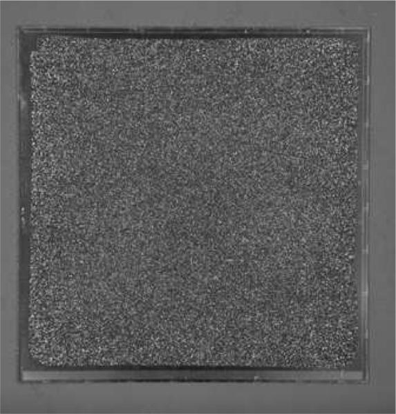
Mercuric iodide-coated 1.2 cm × 1.2 cm readout mounted on a PCB. Coated area is about 1 cm × 1 cm. Readout is a 400x400 array of 30 μm × 30 μm pixels. Electronic schematic is the same as for the 3200×3200 array shown in Figs. 3 and 4, duplicating all circuitry except the size of the sensitive area.
VI. Results
A. X-ray Planar Images
Figs. 6-8 show several planar x-ray images from a 400×400 pixel HgI2-coated array such as the one shown in Fig. 5. Since the top electrical contact on this imager was smaller than the coated area, the response was limited to the central ∼7 mm × 7 mm region. Horizontal line profiles through a spatial resolution phantom image at the 4 and 5 lp/mm resolution levels are shown in Fig. 7. Based on these line profiles, we estimate that the MTF at 5 lp/mm is about 0.6.
Fig. 6.

X-ray images from HgI2-coated CMOS readouts such as the one shown in Fig. 5. Bolt (left) has thread spacing of about 470 μm. Saw blade (right) has peak-to-peak spacing of about 2.4 mm. Image exposure was 200 ms, bias applied was 0.12 V/μm with a film thickness of about 200 μm. X-ray generator was set to 70 kVp and 10 mA, with 2 mm of Al filter; offset and gain correction were applied.
Fig. 8.

Planar x-ray image of a slit. Top: Section of image produced by a slit in Pb plate placed on top of the HgI2−coated CMOS readout and illuminated by x-ray flood. Bottom: Vertical line profile at the point indicated by the arrow in the top image. Slit width is ∼50 μm. Line profile exhibits a FWHM of ∼80 μm. Imager is as shown in Fig. 5. One pixel unit is 30 μm. Image exposure was 400 ms, bias applied was 0.2 V/μm with a film thickness of about 200 μm. X-ray generator was set to 70 kVp and 10 mA, with 2 mm of Al filter; offset and gain correction were applied.
Fig. 7.

X-ray image of a spatial resolution phantom (Nuclear Associates) from a HgI2-coated CMOS readout such as the one shown in Fig. 5. Line profiles at the 5 line pair/mm and 4 lp/mm levels demonstrate the spatial resolution in this prototype imager. One pixel unit is 30 μm. Image exposure was 200 ms, bias applied was 0.1 V/μm with a film thickness of about 200 μm. X-ray generator was set to 70 kVp and 10 mA, with 2 mm of Al filter; offset and gain correction were applied.
The top part of Fig. 8 shows a planar x-ray image of a slit cut into a 0.5 mm thick Pb panel. Since the slit was created by a crude cutting process, the slit width varies along its length, and the slit walls exhibit some burs. However, optical measurement of the slit width at the point indicated by the arrow showed the slit width to be ∼50 μm. A line profile across the slit x-ray image along a vertical line at this point is shown at the bottom of Fig. 8. The FWHM of the profile is about 80 μm, demonstrating that the imager is capable of high resolution imaging.
Although the Nyquist frequency for the CMOS readouts with 30 μm pixel pitch is 17 lp/mm, allowing very high resolution imaging, we observe that the spatial resolution at higher values is degraded in some regions by nonuniform crystal sizes in the polycrystalline film, leading to some areas where charge is shared across groups of pixels, and by the presence of isolated pixels and groups of pixels which are not electrically connected to the film. Our recent efforts are to reduce these effects by modifying the pretreatment of the CMOS readouts before film growth to further promote film adhesion and uniform small crystal size film growth. Full characterization of these films at the higher resolution values which are consistent with the small pixel sizes of the readouts is planned.
To put this work into the context of other efforts to create x-ray imagers with polycrystalline semiconductor detectors grown on pixilated readouts, we present a few results from a-Se-, PbI2−, and CZT-based systems. Note that polycrystalline TlBr has not been grown directly onto readouts and results have been limited to a few larger pixels (see [23]), so we do not present TlBr results here.
Choquette et al. [24] have described a flat panel system based on a 1 mm thick a-Se film with an MTF of 0.63 at the Nyquist frequency of 3.3 lp/mm (150 μm pixel grid). Sensitivity was 4.4 μC/Rcm2 with a corresponding dark current of 0.1 nA/cm2. Zentai et al. [11] presented the imaging characteristics of a PbI2-based system with a 100 μm thick film deposited on a TFT readout. At the Nyquist frequency of 3.9 lp/mm (127 μm pixel pitch), the MTF was about 0.4. The maximum sensitivity was about 10 μC/Rcm2 with a corresponding dark current of 2.7 nA/cm2. Tokuda et al. [25] have grown a 314 μm-thick polycrystalline CZT film by the closed-space sublimation process. They measured an MTF of about 0.3 at the Nyquist frequency of 3.3 lp/mm for their 150 μm pixel grid TFT readout. Sensitivity was measured as 24 μC/Rcm2 with a corresponding dark current of 7 nA/cm2. However, the film was not grown directly onto the readout structure; instead, it was grown onto a substrate with a uniform conductive coating. Then conductive resin patches were emplaced at each pixel on the readout and the film/substrate assembly was placed onto the readout to achieve a pixilated system. This process is more complex than direct film growth onto readouts, and it requires the lapping and polishing of the deposited film.
The HgI2/CMOS readout we have described here has a Nyquist frequency of 17 lp/mm (30 μm pixel pitch) with an estimated MTF of about 0.6 at 5 lp/mm. Using the same x-ray illumination as specified in Figs. 6-8, we measured x-ray sensitivity of 6.2 μC/Rcm2 with corresponding dark current of ∼2.7 nA/cm2.
B. X-ray CT Images
One of the 400×400 pixel HgI2−coated arrays was placed into a commercial small-animal x-ray CT gantry, shown in Fig. 9, and used to image small-diameter tungsten wires suspended in air. X-ray projections were collected in a step-and-shoot CT scan. The reconstructions were performed with a Feldcamp cone beam filtered back projection algorithm. A trans-axial slice through each of the resulting reconstructed 3D data sets is shown in Fig. 10.
Fig. 9.

Small-animal x-ray CT system with HgI2-coated CMOS readout installed for phantom imaging. This preclinical imaging system is the commercially-available X-SPECT™ from Gamma Medica-Ideas, Inc. (Northridge, CA).
Fig. 10.

Reconstructed CT images of a 200 μm diameter tungsten wire (left) and a 50 μm diameter tungsten wire (right). Imaging was performed by a HgI2−coated CMOS readout array like the one shown in Fig. 5, installed in a commercial preclinical x-ray CT gantry as shown in Fig. 9.
The reconstructed image of a 200 μm diameter tungsten wire (left side, Fig. 10) acquired with the HgI2/CMOS detector was obtained at x-ray tube settings of 60 kVp and 0.2 mA. The imaging parameters for the CT scan would have produced an absorbed dose for a mouse of approximately 0.01 cGy. Such low-dose scanning is desirable for longitudinal mouse studies where the subject is scanned multiple times.
The reconstructed image of the 50 μm diameter tungsten wire (right side, Fig. 10) acquired with the HgI2/CMOS detector was obtained at x-ray tube settings of 60 kVp and 6.5 mA. Horizontal and vertical line profiles through the center of the image of the smaller wire demonstrate 70 μm FWHM which indicates that the point spread function at this tube current is sufficient to obtain a 50 μm spatial resolution in reconstructed CT images. The imaging parameters for the CT scan would have produced an absorbed dose for a mouse of approximately 1.3 cGy. An equivalent scan using the same equipment except replacing the HgI2 detector with a commercially-available phosphor-coated readout is estimated to produce an absorbed mouse dose of about 10 cGy [26].
VII. Summary
Polycrystalline HgI2 was grown directly onto CMOS readout arrays with 30 μm pixel grids using low-temperature thermal vapor transport. Initial results from prototype 400×400 pixel readouts coated with 200 μm thick HgI2 demonstrate imaging capability but are limited by some regions with nonuniform crystallite size and by the presence of some unresponsive pixels. The devices exhibited sensitivity of 6.2 μC/Rcm2 with corresponding dark current of ∼2.7 nA/cm2, and a 80 μm FWHM planar image response to a 50 μm slit aperture. X-ray CT images demonstrate a point spread function sufficient to obtain a 50 μm spatial resolution in reconstructed CT images at a substantially reduced dose compared to phosphor-coated readouts. Future plans are to modify the readout array pretreatment to promote film adhesion and uniform small crystal size film growth. These xray imagers have potential as efficient and high-resolution detectors for applications such as intraoral dental imaging, small-animal x-ray CT, and, when extended to larger readouts, planar chest x-ray imaging.
Acknowledgments
This work was supported in part by the U.S. National Institutes of Health under Grant Nos. 2R44EB003058 and 1R43DE017846.
References
- 1.Schieber M, Carlston RC, Lamonds HA, Randtke PT, Schnepple FW, Llacer J. Purification, growth, and characterization of alpha mercuric-iodide crystals for gamma-ray detection. J. Cryst. Growth. 1974;24/25:205–211. [Google Scholar]
- 2.Iwanczyk JS. Advances in mercuric iodide x-ray detectors and low noise preamplification systems. Nucl. Instrum. Methods. 1989;A283:208–214. [Google Scholar]
- 3.Burger A, Nason D, van den Berg L, Schieber M, Schlesinger TE, et al. Semiconductors for Room Temperature Nuclear Detector Applications. Academic Press; San Diego: 1995. Growth of mercuric iodide; pp. 85–110. [Google Scholar]
- 4.Constellation Technology Corporation. http://www.contech.com/
- 5.Lamonds HA. Review of mercuric iodide development program in Santa Barbara. Nucl. Instrum. Methods. 1983;213:5–12. [Google Scholar]
- 6.Iwanczyk JS, Patt BE, Tull CR, MacDonald LR, Skinner N, Hoffman EJ, et al. Mercuric iodide polycrystalline films. Proc. SPIE. 2001;4508:28–40. [Google Scholar]
- 7.Schieber M, Hermon H, Zuck A, Vilensky A, Melekhov L, Shatunovsky R, Meerson E, Saado H. Polycrystalline mercuric iodide detectors. Proc. SPIE. 1999;3770:146–155. [Google Scholar]
- 8.Schieber M, Zuck A, Gilboa H, Zentai G. Reviewing polycrystalline mercuric iodide x-ray detectors. IEEE Nucl. Sci. Symp. & Med. Imag. Conf. 2004:4327–4331. [Google Scholar]
- 9.Hartsough NE, Iwanczyk JS, Patt BE, Skinner NL. Imaging performance of mercuric iodide polycrystalline films. IEEE Trans. Nucl. Sci. 2004;51:1812–1816. [Google Scholar]
- 10.Zentai G, Partain L, Pavlyuchkova R, Proano C, Virshup G, Breen BN, Vilensky A, Dagan O, Meerson E, Schieber M, Gilboa H, Thomas J. Detailed imager evaluation and unique applications of a new 20 cm × 25 cm size mercuric iodide thick film x-ray detector. Proc. SPIE. 2003;5047:84–95. [Google Scholar]
- 11.Zentai G, Partain L, Pavlyuchkova R, Proano C, Schieber M, Shah K, Bennett P, Melekhov L, Gilboa H. Comparison of mercuric iodide and lead iodide x-ray detectors for x-ray imaging applications. IEEE Trans. Nucl. Sci. 2006;53:2506–2512. [Google Scholar]
- 12.Street RA, Mulato M, Ready SE, Lau R, Ho J, Van Schuylenbergh K, Schieber M, Hermon H, Zuck A, Vilensky A, Shah K, Bennett P, Dmitryev Y. Comparative study of PbI2 and HgI2 as direct detector materials for high resolution x-ray image sensors. Proc. SPIE. 2001;4320:1–12. [Google Scholar]
- 13.Nygard E. U.S. Pat. # 7132637 Pixel sensor having a layer of sensor material grown on a pre-fabricated wafer and method of manufacture thereof.
- 14.Jing T, Cho G, Drewery J, Fujieda I, Kaplan SN, Mireshghi A, Perez-Mendez V, Wildermuth D. Enhanced columnar structure in CsI layer by substrate patterning. IEEE Trans. Nucl. Sci. 1992;39:1195–1198. [Google Scholar]
- 15.Knoll GF. Radiation Detection and Measurement. John Wiley and Sons, Inc.; New York: 1989. [Google Scholar]
- 16.Iwanczyk JS, Patt BE. Comparison of HgI2, CdTe, and Si(PIN) x-ray detectors. Nucl. Instrum. Methods. 1996;A380:186–192. [Google Scholar]
- 17.Baciak JE, He Z. Long-term stability of 1-cm thick pixelated HgI2 gamma-ray spectrometer operating at room temperature. IEEE Trans. Nucl. Sci. 2004;51:1886–1894. [Google Scholar]
- 18.Meng LJ, He Z, Alexander B, Sandoval J. Spectroscopic performance of thick HgI2 detectors. IEEE Trans. Nucl. Sci. 2006;53:1706–1712. doi: 10.1109/TNS.2006.873714. [DOI] [PMC free article] [PubMed] [Google Scholar]
- 19.Owens A, Andersson H, Bavdaz M, van den Berg L, Peacock A, Puig A. The hard x-ray response of a large area HgI2 detector. Nucl. Instrum. Methods. 2002;A487:90–95. [Google Scholar]
- 20.Gerrish VM, Schlesinger TE, et al. Semiconductors for Room Temperature Nuclear Detector Applications, 1st ed. Academic Press; San Diego: 1995. Characterization and quantification of detector performance; pp. 493–530. [Google Scholar]
- 21.Skinner N, Ortale C, Schieber M, van den Berg L. Modified purification of mercuric iodide for crystal growth. J. Cryst. Growth. 1988;89:86–92. [Google Scholar]
- 22.Skinner NL, Ortale C, Schieber M, van den Berg L. Preparation and evaluation of mercuric iodide for crystal growth. Nucl. Instrum. Methods. 1989;A283:119–122. [Google Scholar]
- 23.Onodera T, Hitomi K, Shoji T, Hiratate Y, Kitaguchi H. Spectroscopic performance of pixellated thallium bromide detectors. IEEE Trans. Nucl. Sci. 2005;52:1999–2002. [Google Scholar]
- 24.Choquette M, Rougeot H, Martin JP, Laperriere L, Shukri Z, Polischuk BT. Direct selenium x-ray detector for fluoroscpy, R&F, and radiography. Proc. SPIE. 2000;3977:128–136. [Google Scholar]
- 25.Tokuda S, Kishihara H, Adachi S, Sato T. Preparation and characterization of polycrystalline CdZnTe films for large-area, high-sensitivity x-ray detectors. Journal of Materials Science: Materials in Electronics. 2004;15:1–8. [Google Scholar]
- 26.Li J. Personal Communication. Gamma Medica-Ideas, Inc.; 2009. [Google Scholar]