Abstract
Nanofluidics represents a promising solution to problems in fields ranging from biomolecular analysis to optical property tuning. Recently a number of simple nanofluidic fabrication techniques have been introduced that exploit the deformability of elastomeric materials like polydimethylsiloxane (PDMS). These techniques are limited by the complexity of the devices that can be fabricated, which can only create straight or irregular channels normal to the direction of an applied strain. Here, we report a technique for nanofluidic fabrication based on the controlled collapse of microchannel structures. As is demonstrated, this method converts the easy to control vertical dimension of a PDMS mold to the lateral dimension of a nanochannel. We demonstrate here the creation of complex nanochannel structures as small as 60 nm and provide simple design rules for determining the conditions under which nanochannel formation will occur. The applicability of the technique to biomolecular analysis is demonstrated by showing DNA elongation in a nanochannel and a technique for optofluidic surface enhanced Raman detection of nucleic acids.
Keywords: concentrator, nanofluidic channel, single molecule manipulation, surface enhanced raman scattering
Of the many reasons why nanofluidic (1–8) systems are of interest, the most well developed applications revolve around sensing, detection, and species handling in single or “few” molecule environments. Researchers have recently demonstrated unique bioanalytical capabilities in nanofluidic devices including the ability to elongate single DNA molecules (2), concentrate protein samples by more than four orders of magnitude (9), and efficiently separate both large (3, 10) and small (4) biomolecules. As a result of their technological promise, numerous methods have been developed to fabricate these systems, including electron beam lithography (11, 12), focused ion beam milling (13), interference lithography (14), AFM lithography (15), and nano-imprint lithography (2, 16). The significant advantages of these high-end nanofabrication technologies are their high resolution, reproducibility, and flexibility. Despite these advantages, these methods are somewhat limited when it comes to rapid prototyping of nanofluidic systems. To augment these high-resolution techniques, several groups have developed simpler nanofluidic fabrication in polydimethylsiloxane (PDMS) using lower resolution lithography methods. Huh et al. (17) for example used crack formation in a surface oxide layer to make nanochannels with mechanically tunable widths. Similarly, Chung et al. (18) used wrinkles on an elastomeric PDMS surface that, when bonded to another surface, formed discrete nanochannels. While these approaches greatly simplify the fabrication of nanochannels, the complexity of the devices that can be created is relatively low, in that only straight lines orthogonal to the stretching force can be fabricated.
An additional challenge of nanofluidic fabrication with soft materials like PDMS is the relatively low stiffness of the material resulting in dimensional instability and even channel collapse to the point of sealing (19). With the goal of determining the design rules that minimize these effects, Huang et al. (20, 21) recently reported on the mechanism of channel collapse (also referred to as “roof” or “stamp” collapse) in soft lithography. Their work characterized many of the conditions under which the middle of a suspended channel structure will sag to the point of touching the lower substrate and permanently seal. Ultimately, the use of PDMS with higher stiffness or channel designs with a close to square cross section have been found to be good techniques to minimize these problems (17, 22, 23).
In this paper, we demonstrate a method by which this channel collapse technique can be exploited as a simple method for rapid prototyping complex nanofluidic systems. Here, we show that under controllable conditions, the system can be made to collapse in such a way so as to leave nanofluidic channels as small as 60 nm from low resolution, but highly complex, photolithographic patterns. The material stiffness and geometric conditions that lead to this collapse are characterized along with how these parameters can be varied to obtain desired nanochannel sizes. The usefulness of this method to practical nanofluidic system development is demonstrated by creating devices for DNA elongation, nanofluidic concentration, and surface-enhanced Raman scattering (SERS)-based detection of nucleic acids.
Results
Nanochannel Formation and Characterization.
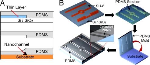
Our approach to nanochannel formation is shown schematically in Fig. 1. Details of the fabrication process are provided in the Materials and Methods section, however, briefly the desired PDMS microchannels are obtained using patterned metal or SU-8 masters and traditional soft lithography processes (24). Under the proper conditions (characterized below), when placed in conformal contact, the microchannel will collapse, and the roof will bond to the lower substrate. By controlling the thickness of the master, the width of the channel feature and the elasticity of the PDMS with various elastomer base/curing agent ratios, we are able to create a large range of nanochannel sizes, shapes, and fluidic layouts (see Fig. S1).
Fig. 1.
Schematic describing “roof-collapse” technique for nanochannel fabrication. (A) Two-dimensional representation of the fabrication process. For clarity, the thicknesses of the various layers on the substrate are not drawn to scale. A thin layer of photoresist or evaporated metal is deposited on the substrate and lithographically pattered to the desired channel layout. Since the channel size is dependent on the height of the master, the resolution with which the channels can be patterned is not important. Patterning different thicknesses allows interfacing of different channel size. After patterning, the PDMS solution is cast onto the master. The PDMS mold is then removed and bonded to a plain substrate. (B) Three-dimensional representation of the fabrication process. Various pattern shapes can be used as a nanochannel template. “Roof collapse” of the PDMS leaves behind a nanochannel at the edge. Inset indicates triangular shape nanochannels were formed after the roof collapse.
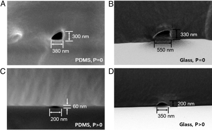
To measure the dimensions of the fabricated devices, scanning electron microscopy (SEM) image analysis of fractured nanochannels cross-section was performed (see Materials and Methods section for details). Sample cross-sectional images of four different types of nanochannel systems are shown in Fig. 2, namely (Fig. 2A) PDMS/PDMS, (Fig. 2B) PDMS/glass, (Fig. 2C) PDMS/PDMS with 50 kPa compressive pressure applied from above, and (Fig. 2D) PDMS/glass also with the external applied pressure. Most nanochannels fabricated by this approach had a triangular cross-section (as in Fig. 2 A and B), the exception being those subject to a compressive force which were generally semicircular (Fig. 2 C and D). The applied compressive stress also served to shrink the width and height of the nanochannel. The PDMS/PDMS channels shown in Fig. 2 A and C were fabricated under the same master height (700 nm) and elastomer base/curing agent conditions (10:1). The uncompressed channel has a cross-section with dimensions of 380 nm (width) by 300 nm (height). When the compressive stress is applied, the channel height (normal to the pressure direction) is shown to shrink by ≈5-fold to 60 nm and the channel width reduced to 200 nm. The compressed nanochannels were formed right after the oxidizing treatment, and thus it is believed that this process should be irreversible so that the final dimension of the nanochannels remains dimensionally stable. As can also be seen in Fig. 2, in both the compressed and uncompressed cases, the use of a stiffer lower substrate (glass vs. PDMS) tended to result in channels with larger widths and heights.
Fig. 2.
SEM images of nanochannels. (A) Bonding of a PDMS (mold) to a PDMS (substrate) results in nanochannels with a triangular cross-section. (B) PDMS (mold)-cover glass (substrate) bonding results in larger channel width due to its elastic moduli mismatch. (C) With a controlled 50 kPa normal stress is applied to a PDMS (mold)-PDMS (substrate) system, much smaller channels result. The same PDMS mold as (A) was used to form the smaller channel shown here. (D) Compressed nanochannel in PDMS (mold)-cover glass (substrate). Again the same PDMS mold as (B) was used.
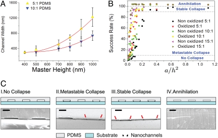
To determine the dependence of master height and material elasticity on the formed nanochannel width, we performed a number of experiments using masters with a range of heights (300, 400, 500, 700, 800, 900, and 1,000 nm) and PDMS with different elastomer base/curing agent ratios (5:1, 10:1, and 15:1). We would expect the width and height of the nanochannel to be smaller for shorter master heights and greater elastomer base/curing agent ratios [or equivalently greater elasticity (25)]. From the theory developed by Huang et al. (20) and Zhou et al. (21), we expect the unsagged length of the PDMS (which in this case represents the final nanochannel width, L) to be proportional to the elastic modulus, E, times the square of the master height, h or L ∝ Eh2. As can be seen in Fig. 3A, our results agree with this quadratic relation. According to Wilder et al. (25), 5:1 PDMS has a larger elastic modulus (≈2.6 MPa) than that of 10:1 PDMS (≈1.6 MPa). Using a nonlinear least-squares algorithm to fit both curves from Fig. 3A, we were able to obtain a ratio of elastic moduli for 5:1 and 10:1 PDMS of 1.58, which is similar to that obtained from Wilder et al.'s results (1.63) (25). We note that even though the oxidation of the PDMS surface resulted in more stable formation of nanochannels, it did not affect the final dimension of the formed nanochannels (see Fig. S2).
Fig. 3.
Nanochannel characterizations. (A) Channel width is plotted against master's height for both 10:1 PDMS and 5:1 PDMS. Due to their different elastic moduli, generally 10:1 PDMS nanochannel yields smaller widths than that of 5:1. (B) The nanochannel formation rate is characterized as a function of a/h2, for different elastic moduli (5:1, 10:1, and 15:1) and oxidized vs. non-oxidized PDMS. Each dash line represents the “No collapse,” “Metastable collapse,” “Stable collapse,” and “Annihilation” regions. (C) Schematic representations of four regions in (B). Each region is accompanied with its SEM counterpart. The red arrows indicate the location of the nanochannels (Scale bars, 10 μm).
Generally speaking, there were two cases where nanochannels formation was not successful: When the formed microchannel failed to collapse and when the collapse resulted in complete sealing or annihilation of the desired structure. To quantify the conditions that resulted in high device yields, we performed experiments under different fabrication conditions to obtain a “nanochannel formation success rate,” which is defined as the percentage of channels in which stable roof collapse was observed (see Table S1 for complete experimental results). In Fig. 3B, we plot this parameter as a function of the original masters' width, a, divided by its height, h, squared. The a/h2 parameter is proportional to the work required to achieve contact between the PDMS mold and the lower substrate according to Huang et al. (20). As with the above, in addition to the geometric parameters, we also considered other variables including the surface energy of the PDMS mold and substrate (i.e., with and without plasma oxidation) and the elastomer base/curing agent ratio. In all these experiments, the nanochannel formation success was gauged using SEM and optical microscopy.
On the basis of these results, four regions could be identified: a no-collapse region for weak adhesion (<10% success rate of nanochannel formation); a metastable collapse region for intermediate adhesion (<90% success rate of nanochannel formation); a stable, high-yield, collapse region for strong adhesion (>90% collapse); and an annihilation region in which the nanochannels disappeared. As can be seen in Fig. 3B, for all cases as the work of adhesion increased, the nanochannel formation success rate also increased. Successful nanochannel formation of 5:1 and 10:1 PDMS remained below 10% yield until approximately a/h2 = 0.1. Above a/h2 = 0.2, the success rate of nanochannel formation was around 90%. The formed nanochannels started to disappear (annihilation) above a/h2 = 0.3 due to complete collapse of the channel. As can also be seen, greater nanochannel formation rates were generally observed when PDMS molds with greater elasticity were used (elastomer base/curing agent ratios of 15:1 and 10:1) than with the stiffer material. This is because the deformation energy of the PDMS mold increases as the stiffness of PDMS decreases. Similarly, due to the higher surface energy of the PDMS mold and the substrate, the oxidized PDMS mold resulted in a higher success rate of nanochannel formation. Based on these experimental results, we used master geometries ranging from 500 to 700 nm in height, from 10 to 100 μm in width, and from 5:1 to 10:1 oxidized PDMS for the remainder of the devices used in this study.
Nanofluidic and Single Molecule Manipulation.
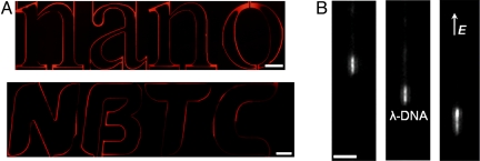
To test the fluidic continuity of the formed nanochannels, we filled them with a solution of 100 μM Rhodamine B in 50:50 isopropanol/water and imaged them using an optical microscope (Olympus IX-70 microscope; Olympus). As is shown in Fig. 4, we used straight nanochannels as well as a number of more complicated designs (see Fig. S3). This demonstrates the ability of the technique to create nanofluidic systems with arbitrary layouts using low-resolution optical lithography.
Fig. 4.
Optical images of complex nanochannels (A) and manipulation of a single DNA molecule along a straight nanochannel (B). (A) Nanofluidic representations of “nano” and “NBTC” (the logo of the Nanobiotechnology Center from Cornell University). Complex nanofluidic networks are possible with this technique. All these nanochannels are formed with at least one axis in nanometer regime (Scale bar, 100 and 50 μm, respectively). For a demonstration purpose, each letter is taken individually and then combined together. (B) Electrophoretic migration of the λ-DNA in a straight nanochannel by 40 V cm-1 (0.5-s interval between the images.) Electric field is represented by E (Scale bar, 5 μm).
To demonstrate the practical application of these devices to single molecule analysis, we imaged individual DNA molecules in solution as they passed through the nanochannels (see Fig. 4B and Fig. S4 A–C, and additional details on the preparation of the DNA are provided in the Materials and Methods section). The device used here had two large reservoirs (2 cm × 5 mm × 10 μm deep) connected by nanochannels formed via the collapsing method described above. When electrophoretically driven into the nanochannels, the DNA molecules stretched to ≈5 μm in length, which is ≈25% of their full contour length. The full contour length of 48.5 kb λ-DNA can be calculated from the base pair spacing of 0.34 nm and the additional 30% increase caused by intercalation of the YOYO-1 dye (12) resulting in approximately 20 μm. Assuming that the root mean square end-to-end length of DNA, Lz, obeys Flory-Pincus scaling, it has been shown that Lz = L(pw)1/3d-2/3, where p is the persistence length, w is the molecule width, L is the contour length, and d is the nanochannel width (2). Using this relation, we can extract the nanochannel width from the observed contour length of λ-DNA as it travels along the length of the nanochannel. Fig. 4B illustrates the motion of a DNA molecule under an electric field in the nanochannels at three different locations. As is shown in these images, the stretched length did not vary significantly along the length of the channel, suggesting that the formed channels are both continuous and uniform along their length. Based on the above theory, the observed length of 5 μm indicates that the confined nanochannel width is ≈200 nm in one axis (see Fig. S4B). We note that this is consistent with the 8-μm contour length observed by Tegenfeldt et al. (2) for 100-nm channels.
Interfacing Micro- and Nanofluidic Structures and Demonstration of a Concentration Device.
From an integrated device point of view, it is of interest to integrate nanofluidic elements (which enable single molecule manipulations such as that shown above) with larger and more complex microfluidic structures that can facilitate high-throughput or automated processing. In practice, this is often difficult to achieve because of mismatches in the fabrication technologies required. For example, nanofluidics may have been fabricated using electron-beam lithography, and the resulting structure aligned and assembled with another device fabricated using optical lithography. Mismatches between the materials compatible with each process and the difficulty in aligning microscale features with nanoscale ones, often makes this a difficult challenge. By simply changing an a/h2 value at the interface, our technique can be used for rapid prototyping as well as enabling facile interfacing of micro- and nanofluidic elements.
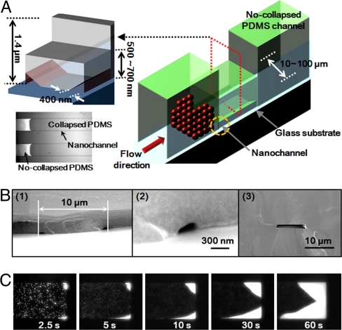
To demonstrate this here, we have developed a simple sample concentration device that allows for rapid sample enrichment at a micro-/nanofluidic interface. Fig. 5A shows a schematic representation of the device that was constructed by interfacing a single layer thick master with one that was twice as thick. Equivalent results could be achieved by using mismatched widths as well. As is shown in Fig. 5B, after casting the master in PDMS, the thin channel section formed two nanochannels (400 nm wide × 300 nm high), which was interfaced with a single microchannel (10 μm wide × 1.4 μm high). To characterize the concentration capability of this device, negatively charged fluorescent polystyrene nanoparticles with diameters of 700 and 45 nm in an aqueous solution were introduced into the microchannel and caused to flow downstream electrophoretically through the application of an external electric field with a strength of 40 V/cm. Fig. 5C shows the accumulation of 700-nm nanoparticles at the nanofluidic interface over the course of 60 s. By comparing the emitted florescent intensity in the concentration region with that in the normal flow, we estimate at least a 30-fold concentration of the particles in 1 min. We also successfully demonstrated the concentration of 45-nm nanoparticles at the interface (see Fig. S4D).
Fig. 5.
Interfacing nanofluidics with microfluidics and demonstration of a nanofluidic concentration device. (A) The nanofluidic concentration system used here consists of two functionally interfaced channels: A micrometer scale channel fabricated from a double thickness master and two nanoscale channels fabricated from the collapse of a single layer thickness master. Schematic representation of the operation of the device shows the concentration of nanoparticles at the interface between the microchannel and the nanochannel. (B) SEM images of (1–2) the nanofluidic channel (400 nm width × 300 nm height) and (3) microfluidic channel (10 μm width × 1.4 μm height). (C) Time-lapse images of concentration of 700-nm polystyrene nanoparticles at the interface between microchannel and nanochannel.
SERS-Based Detection of Nucleic Acids.
To demonstrate the use of the approach to biomolecular detection, we applied the concentration device shown above to SERS-based detection of nucleic acids. In a number of recent studies (26–28), metal colloid aggregation and concentration has been shown to significantly enhance the sensitivity and reproducibility of SERS-based measurements. Chou et al. (29) for example recently reported a device that trapped metal nanoparticles at a microchannel-nanochannel junction, which has the coupled effect of both increasing the intensity of the surface plasmon field (through multiparticle interactions) and the number of local emitters ultimately yielding an enhanced limit of detection for solution phase β-amyloids. As another example, Choi et al. (30) investigated an optofluidic compact disc (CD) platform. This device allows the accumulation of target molecules and SERS enhancers via centrifugal force.
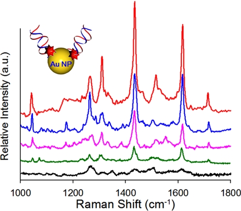
Here we demonstrate the applicability of our rapid prototyping technique to biomolecular sensing through the development of a SERS-based detection technique enhanced by the nanofluidic concentrator device described above. As with the above, the advantage here is that the device can be fabricated simply by controlling the a/h2 aspect ratio of the channels and allowing for elastomeric collapse without requiring additional processes. We apply our device in a similar way to detect nucleic acid sequences associated with Dengue virus serotype 4 (DENV-4). Dengue virus is an acute febrile viral disease characterized by sudden fever and onset, and there are four different serotypes (DENV-1–4) (31). In this experiment, we first fill the same micro-/nanofluidic concentrator device described above, via capillary force, with an aqueous solution of gold nanoparticles functionalized with nucleic acid sequences specific to DENV-4 (see Materials and Methods section for details). After filling, the negatively charged gold nanoparticles are concentrated at the entrance of the nanofluidic channel by applying the same 40 V/cm electric field used above for as long as 60 s. To obtain the SERS signals from the resulting nanoparticle cluster, the excitation laser was focused at the micro/nanochannel interface, and the emission spectrum was recorded between a wave-number range of 1,000 to 1,800 cm-1 using a 15-s integration time. The resulting SERS spectra of Cy3-labeled DENV-4a is shown in Fig. 6, collected for concentration times ranging from 5 to 60 s. As seen in Fig. 6, our results show that the correct spectroscopic fingerprints corresponded to Cy3-labeled dye (32) and that the intensity increases with the accumulation time, as expected.
Fig. 6.
SERS spectra of 3 nM Cy3-labeled DENV-4a. After introducing the 60-nm Au colloid solution by applying electric field of 40 V cm-1, the SERS emission at the interface between nanochannels and microchannel was monitored as a function of time: (1) 5 s, (2) 10 s, (3) 20 s, (4) 40 s, and (5) 60 s. As expected, the intensity of the signal increases with the accumulation and aggregation of SERS emitters.
Discussion
PDMS is a popular material for rapid prototyping of microfluidics, due to its easy patterning, optical transparency, and flexibility (33–36). Here, we have demonstrated and characterized a technique for the creation of nanofluidic systems based on the controlled elastomeric (PDMS) collapse. Our approach combines the dimensional range and network complexity that can be obtained from high-end nanofabrication techniques with the simplicity of recently demonstrated nonlithographic approaches to rapid prototyping of nanofluidic devices.
To achieve nanofluidic systems embedded in a PDMS microfluidic format, a variety of methods have been reported including reversible bonding between glass and PDMS (37), the junction gap breakdown of PDMS at high voltages (9) and nanocapillary array integration (38). However, these methods led to relatively poor coupling between microstructures and nanoscale structures. The approach developed here greatly facilitates this. By building some structures with an a/h2 value in the range in which nanochannels formation is highly likely and others where this value is in the range where collapse will not happen (leaving behind a microchannel), a facile interface between the two is guaranteed.
In summary, while PDMS generally been considered a polymeric platform for microscale structures, our approach expands its horizon from micro to nanoscale platform, enabling rapid prototyping of a wide range of geometries. Another advantageous feature of our approach is its design flexibility. We note that because the nanochannel layout matches that of its master, the nanochannels can be formed into complex patterns (so long as the master holds a looped curve). Because the master can be freely designed with basic low-resolution photolithography, we note that a major strength of this method is that it affords a large degree of freedom in designing functional nanofluidic structures, as opposed to previous approaches, which only enable straight lines. We envision that this form of nanofabrication could strongly facilitate the rapid prototyping of a variety of nanofluidic devices.
Materials and Methods
Fabrication of PDMS Nanochannels.
Fig. 1 shows a schematic of the nanochannel fabrication processes. First, the desired pattern was made on a silicon wafer using standard photolithography processes. Negative photoresist SU-8 (Microchem) 2000.5, 2002, and 2007 were used for different heights of the master in the range from 300 nm to 10 μm. The PDMS base to curing agent ratios were varied with 15:1, 10:1, and 5:1 by weight. After mixing the curing agent and elastomer base and degassing the mixture, it was cast onto the premade master and allowed to cure at 80 °C for 4 h. After the PDMS mold was removed from the master, it was bonded to both cover glass and PDMS substrates by plasma oxidation for 30 s. Because the SU-8 film thickness could not be sufficiently well-controlled to enable precise characterization of the master thickness on the resulting nanochannels size, deposited aluminum layers were used as masters for these experiments. In this case, glass substrates (Borofloat wafer; Mark Optics) were covered with a Shipley 1827 photoresist (Microchem). Standard photolithography was used to pattern 100-, 50-, 20-, and 10-μm wide features. Aluminum layers of 300-, 400-, 500-, 700-, 800-, 900-, and 1000-nm thicknesses were deposited onto different glass wafers using an electron beam evaporator, CHA MARK 50 (CHA Industry). After deposition, the photoresist was removed using a lift-off process with Microposit 1165 (Microchem) solvent over a 24-h period. The final surface cleaning step was performed in a bath of acetone and isopropanol under gentle sonication.
Nanochannel Imaging and Characterization.
To measure the cross-sectional dimensions of the nanochannels formed from this approach, fabricated PDMS-PDMS chips and PDMS-cover glass chips were frozen in liquid nitrogen, fractured with a chisel and mallet, coated with a Hummer V Au/Pd Sputtering System (Hummer), and imaged with a scanning electron microscope (SEM; Zeiss Ultra/Supra). Examples of the fractured cross-sectional SEM images are shown in Fig. 2.
Preparation of λ Bacteriophage DNA for Elongation in Nanochannels.
λ Bacteriophage DNA (λ-DNA; New England Biolabs) was labeled with the bis-intercalating dye, YOYO-1 (Molecular Probes), at a nominal labeling ratio of 7.6:1, then introduced to the nanochannel, which has been filled with filtered 5× Tris-borate EDTA (TBE) buffer (Sigma) at a concentration of 50 ng/mL. This buffer solution contains 3% (vol/vol) polyvinylpyrrolidone (Sigma), a surfactant, to prevent the adhesion of the specimen to the surface of the nanochannels. Three percent (vol/vol) β-mercaptoethanol (Sigma) was also added to decrease the photobleaching effect. The sample solution was pipetted into one reservoir, while the other was kept empty so as to induce capillary force filling of the nanochannels and to prevent air bubbles. After 10 min of capillary filling, the other reservoir was also filled with buffer solution. Inert gold wires contacting the solution in the reservoirs were used to apply an electric field over the nanochannels.
Preparation of DNA Hybridization Reaction and Raman Detection.
For the Raman enhancers, 60-nm diameter gold colloid solutions were purchased from Nanocs and were diluted to a final concentration of 0.3 nM in 10 mM PBS buffer solution (0.6 M NaCl, pH 7.4). In this study, oligonucleotides that contain sequences specific to DENV-4 virus RNA were selected as the target analyte and were purchased from Operon Biotechnologies. The capture probe for DENV-4a was 3′-modified with a thiol-modifier containing C3 S-S functionality and had the following sequence: 5′-GAG GAA GCT GTA CTC CTG GTG GAA G C3 S-S-3′. We analyzed the specificity of the SERS detection technique by conducting hybridization reaction using the target DNA of DENV-4a. The target probe was modified with Cy3 dye at the 5′ end. The sequences of DENV-4a oligonucleotides were (Cy3) 5′-CTA GTC CTT CCA CCA GGA GTA CAG CTT CCT CCT GGC TTC G-3′. The italicized portions of the target sequence are the complementary nucleotides to each capture probe. Details regarding the functionalization of the gold nanoparticles and DNA hybridization procedures can be found in our previous works (26). In short, to immobilize the probes, 300 nM thiolated capture DNA were added to 0.3 nM gold colloid solution in PBS buffer solution for 6 h at room temperature, followed by a 1-h exposure to 30 μM carboxy-EG6-undecanethiol to prohibit nonspecific binding. Following this, a centrifugation/resuspension cycle was carried out at 10,000 rpm for 30 min, repeated three times, for the removal of excess reagents. The gold NPs immobilized capture probe were resuspended to the final concentration of 3 nM capture probe in the hybridization buffer. Cy3-labeled target DNA in PBS buffer solution was added to gold nanoparticles functionalized with capture probes. After 12 h, the excess target probes were removed by centrifugation and repeated three times at 10,000 rpm for 30 min. Then, the gold nanoparticles were resuspended in PBS buffer solution and were introduced through the inlet port of the nanofluidic device by applying an electric field of 40 V/cm. Raman spectra were measured with an inVia Raman microscope spectrometer coupled to a Leica microscope. The diode laser used here had an excitation wavelength of 785 nm and operated at ≈5 mW power. Wave-number ranges from 1,000 to 1,800 cm-1 were examined here. A 50× long working distance objective lens was used with a spot size of 2 μm.
Supplementary Material
Acknowledgments.
The authors acknowledge funding from and access to the facilities of the Nanobiotechnology Center (NBTC), an STC Program of the National Science Foundation under Agreement no. ECS-9876771. The authors also appreciate access and use of the Cornell Nanoscale Science and Technology Facility (a member of the National Nanofabrication Users Network), which is supported by the National Science Foundation under grant ECS-9731293. Additional support for this work was provided by the National Institutes of Health-National Institute of Biomedical Imaging and Bioengineering (NIH-NIBIB) under grant no. R21EB007031. We thank Dr. Leon Bellan for help with DNA sample preparation and Prof. Jaebum Choo for SERS analysis.
Footnotes
The authors declare no conflict of interest.
This article is a PNAS Direct Submission.
This article contains supporting information online at www.pnas.org/cgi/content/full/0904004106/DCSupplemental.
References
- 1.Hong JW, Quake SR. Integrated nanoliter systems. Nat Biotechnol. 2003;21:1179–1183. doi: 10.1038/nbt871. [DOI] [PubMed] [Google Scholar]
- 2.Tegenfeldt JO, et al. The dynamics of genomic-length DNA molecules in 100-nm channels. Proc Natl Acad Sci USA. 2004;101:10979–10983. doi: 10.1073/pnas.0403849101. [DOI] [PMC free article] [PubMed] [Google Scholar]
- 3.Han J, Craighead HG. Separation of long DNA molecules in a microfabricated entropic trap array. Science. 2000;288:1026–1029. doi: 10.1126/science.288.5468.1026. [DOI] [PubMed] [Google Scholar]
- 4.Fu J, Schoch RB, Stevens AL, Tannenbaum SR, Han J. A patterned anisotropic nanofluidic sieving structure for continuous-flow separation of DNA and proteins. Nature Nanotech. 2007;2:121–128. doi: 10.1038/nnano.2006.206. [DOI] [PMC free article] [PubMed] [Google Scholar]
- 5.Austin R. Nanofluidics: A fork in the nano-road. Nat Nanotechnol. 2007;2:79–80. doi: 10.1038/nnano.2007.18. [DOI] [PubMed] [Google Scholar]
- 6.Riehn R, et al. Restriction mapping in nanofluidic devices. Proc Natl Acad Sci USA. 2005;102:10012–10016. doi: 10.1073/pnas.0503809102. [DOI] [PMC free article] [PubMed] [Google Scholar]
- 7.Daiguji H, Yang P, Szeri AJ, Majumdar A. Electrochemomechanical energy conversion in nanofluidic channels. Nano Lett. 2004;4:2315–2321. [Google Scholar]
- 8.Cowan ML, et al. Ultrafast memory loss and energy redistribution in the hydrogen bond network of liquid H2O. Nature. 2005;434:199–202. doi: 10.1038/nature03383. [DOI] [PubMed] [Google Scholar]
- 9.Lee JH, Chung S, Kim SJ, Han J. Poly(dimethylsiloxane)-based protein preconcentration using a nanogap generated by junction gap breakdown. Anal Chem. 2007;79:6868–6873. doi: 10.1021/ac071162h. [DOI] [PMC free article] [PubMed] [Google Scholar]
- 10.Chou H-P, Spence C, Scherer A, Quake S. A microfabricated device for sizing and sorting DNA molecules. Proc Natl Acad Sci USA. 1999;96:11–13. doi: 10.1073/pnas.96.1.11. [DOI] [PMC free article] [PubMed] [Google Scholar]
- 11.Reccius CH, Stavis SM, Mannion JT, Walker LP, Craighead HG. Conformation, length, and speed measurements of electrodynamically stretched DNA in nanochannels. Biophys J. 2008;95:273–286. doi: 10.1529/biophysj.107.121020. [DOI] [PMC free article] [PubMed] [Google Scholar]
- 12.Mannion JT, Reccius CH, Cross JD, Craighead HG. Conformational analysis of single DNA molecules undergoing entropically induced motion in nanochannels. Biophys J. 2006;90:4538–4545. doi: 10.1529/biophysj.105.074732. [DOI] [PMC free article] [PubMed] [Google Scholar]
- 13.Cao H, et al. Fabrication of 10 nm enclosed nanofluidic channels. Appl Phys Lett. 2002;81:174–176. [Google Scholar]
- 14.O'Brien Ii MJ, et al. Fabrication of an integrated nanofluidic chip using interferometric lithography. J Vac Sci Technol B. 2003;21:2941–2945. [Google Scholar]
- 15.Pellegrino L, et al. (Fe,Mn)3O4 nanochannels fabricated by AFM local-oxidation nanolithography using Mo/poly(methyl methacrylate) nanomasks. Adv Mater. 2006;18:3099–3104. [Google Scholar]
- 16.Xia Q, Morton KJ, Austin RH, Chou SY. Sub-10 nm self-enclosed self-limited nanofluidic channel arrays. Nano Lett. 2008;8:3830–3833. doi: 10.1021/nl802219b. [DOI] [PubMed] [Google Scholar]
- 17.Huh D, et al. Tuneable elastomeric nanochannels for nanofluidic manipulation. Nat Mater. 2007;6:424–428. doi: 10.1038/nmat1907. [DOI] [PubMed] [Google Scholar]
- 18.Chung S, Lee JH, Moon M-W, Han J, Kamm RD. Non-lithographic wrinkle nanochannels for protein preconcentration. Adv Mater. 2008;20:3011–3016. [Google Scholar]
- 19.Chou SY, Krauss PR, Renstrom PJ. Imprint lithography with 25-nanometer resolution. Science. 1996;272:85–87. [Google Scholar]
- 20.Huang YY, et al. Stamp collapse in soft lithography. Langmuir. 2005;21:8058–8068. doi: 10.1021/la0502185. [DOI] [PubMed] [Google Scholar]
- 21.Zhou W, et al. Mechanism for stamp collapse in soft lithography. Appl Phys Lett. 2005;87:251925–3. [Google Scholar]
- 22.Thangawng AL, Swartz MA, Glucksberg MR, Ruoff RS. Bond-detach lithography: A method for micro/nanolithography by precision PDMS patterning. Small. 2007;3:132–138. doi: 10.1002/smll.200500418. [DOI] [PubMed] [Google Scholar]
- 23.Kang H, Lee J, Park J, Lee HH. An improved method of preparing composite poly(dimethylsiloxane) moulds. Nanotechnology. 2006;17:197–200. [Google Scholar]
- 24.McDonald JC, et al. Fabrication of microfluidic systems in poly(dimethylsiloxane) Electrophoresis. 2000;21:27–40. doi: 10.1002/(SICI)1522-2683(20000101)21:1<27::AID-ELPS27>3.0.CO;2-C. [DOI] [PubMed] [Google Scholar]
- 25.Wilder EA, Guo S, Lin-Gibson S, Fasolka MJ, Stafford CM. Measuring the modulus of soft polymer networks via a buckling-based metrology. Macromolecules. 2006;39:4138–4143. [Google Scholar]
- 26.Huh YS, Lowe AJ, Strickland AD, Batt CA, Erickson D. Surface-enhanced raman scattering based ligase detection reaction. J Am Chem Soc. 2009;131:2208–2213. doi: 10.1021/ja807526v. [DOI] [PMC free article] [PubMed] [Google Scholar]
- 27.Graham D, Thompson DG, Smith WE, Faulds K. Control of enhanced Raman scattering using a DNA-based assembly process of dye-coded nanoparticles. Nature Nanotech. 2008;3:548–551. doi: 10.1038/nnano.2008.189. [DOI] [PubMed] [Google Scholar]
- 28.Piorek BD, et al. Free-surface microfluidic control of surface-enhanced Raman spectroscopy for the optimized detection of airborne molecules. Proc Natl Acad Sci USA. 2007;104:18898–18901. doi: 10.1073/pnas.0708596104. [DOI] [PMC free article] [PubMed] [Google Scholar]
- 29.Chou IH, et al. Nanofluidic biosensing for β-amyloid detection using surface enhanced raman spectroscopy. Nano Lett. 2008;8:1729–1735. doi: 10.1021/nl0808132. [DOI] [PMC free article] [PubMed] [Google Scholar]
- 30.Choi D, Kang T, Cho H, Choi Y, Lee LP. Additional amplifications of SERS via an optofluidic CD-based platform. Lab Chip. 2009;9:239–243. doi: 10.1039/b812067f. [DOI] [PubMed] [Google Scholar]
- 31.Franz AWE, et al. Engineering RNA interference-based resistance to dengue virus type 2 in genetically modified Aedes aegypti. Proc Natl Acad Sci USA. 2006;103:4198–4203. doi: 10.1073/pnas.0600479103. [DOI] [PMC free article] [PubMed] [Google Scholar]
- 32.Cao YC, Jin R, Mirkin CA. Nanoparticles with raman spectroscopic fingerprints for DNA and RNA detection. Science. 2002;297:1536–1540. doi: 10.1126/science.297.5586.1536. [DOI] [PubMed] [Google Scholar]
- 33.Wu H, Odom TW, Chiu DT, Whitesides GM. Fabrication of complex three-dimensional microchannel systems in PDMS. J Am Chem Soc. 2003;125:554–559. doi: 10.1021/ja021045y. [DOI] [PubMed] [Google Scholar]
- 34.Genzer J, Efimenko K. Creating long-lived superhydrophobic polymer surfaces through mechanically assembled monolayers. Science. 2000;290:2130–2133. doi: 10.1126/science.290.5499.2130. [DOI] [PubMed] [Google Scholar]
- 35.Diaz-Quijada GA, Wayner DDM. A simple approach to micropatterning and surface modification of poly(dimethylsiloxane) Langmuir. 2004;20:9607–9611. doi: 10.1021/la048761t. [DOI] [PubMed] [Google Scholar]
- 36.Wilbur JL, Kim E, Younan X, Whitesides GM. Lithographic molding: A convenient route to structures with sub-micrometer dimensions. Adv Mater. 1995;7:649–652. [Google Scholar]
- 37.Kim SM, Burns MA, Hasselbrink EF. Electrokinetic protein preconcentration using a simple glass/poly(dimethylsiloxane) microfluidic chip. Anal Chem. 2006;78:4779–4785. doi: 10.1021/ac060031y. [DOI] [PubMed] [Google Scholar]
- 38.Kim SJ, Han J. Self-sealed vertical polymeric nanoporous-junctions for high-throughput nanofluidic applications. Anal Chem. 2008;80:3507–3511. doi: 10.1021/ac800157q. [DOI] [PMC free article] [PubMed] [Google Scholar]
Associated Data
This section collects any data citations, data availability statements, or supplementary materials included in this article.


