

Abstract
We describe a general method to integrate DNA strands between single-walled carbon nanotube electrodes and to measure their electrical properties. We modified DNA sequences with amines on either the 5′ terminus or both the 3′ and 5′ termini and coupled these to the single-walled carbon nanotube electrodes through amide linkages, enabling the electrical properties of complementary and mismatched strands to be measured. Well-matched duplex DNA in the gap between the electrodes exhibits a resistance on the order of 1 MΩ. A single GT or CA mismatch in a DNA 15-mer increases the resistance of the duplex ~300-fold relative to a well-matched one. Certain DNA sequences oriented within this gap are substrates for Alu I, a blunt end restriction enzyme. This enzyme cuts the DNA and eliminates the conductive path, supporting the supposition that the DNA is in its native conformation when bridging the ends of the single-walled carbon nanotubes.
Since the elucidation of the double helical structure of DNA, scientists have been fascinated by the possibility that the stacked aromatic base pairs of DNA may enable charge transport (CT) over significant distances1–5. The nature of the conductive properties of duplex DNA has consequently attracted substantial interest. Initial solution experiments featured photoinduced DNA-mediated CT between well-defined donor and acceptor sites6–13. Long-range CT has been shown to lead to oxidative damage in DNA over 200 Å away from the bound oxidant14,15 and DNA CT has also been found to be exquisitely sensitive to the integrity of the base-pair stack and to the coupling of the donors and acceptors with the DNA (ref. 10). Furthermore, DNA CT can be attenuated by a single base mismatch16. Indeed, this sensitivity of DNA CT to the integrity of the base-pair duplex has prompted both the consideration of roles for DNA CT within the cell17,18 and the construction of electrochemical DNA-based sensors for mutations, base lesions and protein binding19,20.
Previously, we have described a system for measuring the conductivity of a single molecule covalently immobilized within a nanotube gap21–24. In this system, gaps are formed in single-walled carbon nanotubes (SWNTs) that can be reconnected by one or a few molecules attached to both sides of the gap through amide bond formation. This strategy allows molecules to be wired into metal electrodes by means of robust amide linkages, avoiding the problems commonly associated with suspending DNA between electrodes and forming irreproducible electrical contacts. Moreover, the devices are sufficiently robust that aqueous environments can be used. Using this method we have made molecular devices that are able to change their conductance as a function of pH (ref. 21), and others that are sensitive to the binding between protein and substrate22, or that switch their conductance when the bridging molecules are photoswitched24. Here we describe the first measurements of the conductivity of a single DNA duplex when it is wired into a carbon electrode through covalent bonds.
Numerous CT measurements on DNA strands bridging two electrodes have also been carried out in an effort to establish the conductivity of DNA. These measurements have yielded a remarkably wide range of resistance values (1 to 1 × 10⁷ MΩ)25–31. For example, DNA ropes suspended on a metallic grid were found to behave as a semiconductor with a resistance on the order of 1 MΩ (ref. 25). However, one group initially found wide bandgap semiconducting behaviour for DNA duplexes set between two nanoelectrodes using high-voltage electrostatic trapping26, but later found insulating behaviour for longer strands27. In contrast, in other research it was found possible to induce superconductivity at low temperatures in dehydrated DNA bundles on rhenium/carbon electrodes28.
In general, the variability in the results obtained can be understood by considering the solution experiments, which show that DNA CT depends sensitively upon the integrity of the base-pair stack, the absence of damage within the duplex, and the electrical connections to the duplex. It should be noted that measurements using both conducting atomic force microscopy (AFM)29 and scanning tunnelling microscopy (STM)30–32 under aqueous conditions have recently been carried out and show that well-matched DNA exhibits a low resistance (1–10 MΩ), as well as an increase in resistance with an intervening base mismatch31,32. Also, STM measurements on DNA monolayers have shown effective charge transport for well-matched DNA oriented by the STM tip33. However, none of these measurements was of a single duplex, but instead they were carried out for a collection of duplexes on the surface below the AFM or STM tip. Thus, in the conductivity measurements carried out so far, the integrity of the DNA was not well established, the connections to the duplex were not well defined, or the measurement was not definitively of a single DNA duplex.
Fabrication of the cut SWNT devices has been previously described in detail21–24. In brief, SWNTs were grown using chemical vapour deposition (CVD) on highly doped silicon wafers with 300 nm of thermally grown silicon oxide on their surface. Metal electrodes consisting of 5 nm of Cr overlaid with 50 nm of Au were deposited through a shadow mask onto the carbon nanotubes. The silicon wafer serves as a global back gate for the devices. We then spin-cast a layer of polymethylmethacrylate (PMMA) over the entire device structure and used ultrahigh-resolution electron beam lithography to open a window in the PMMA. This process exposed a section of the SWNT only a few nanometres in length, which was excised with an oxygen ion plasma. The oxidative etching of the carbon nanotube generated carboxylic acid functionalities on both sides of the gap (Fig. 1a), which can be bridged with amine-terminated molecules.
Figure 1. A method to cut and functionalize individual SWNTs with DNA strands.
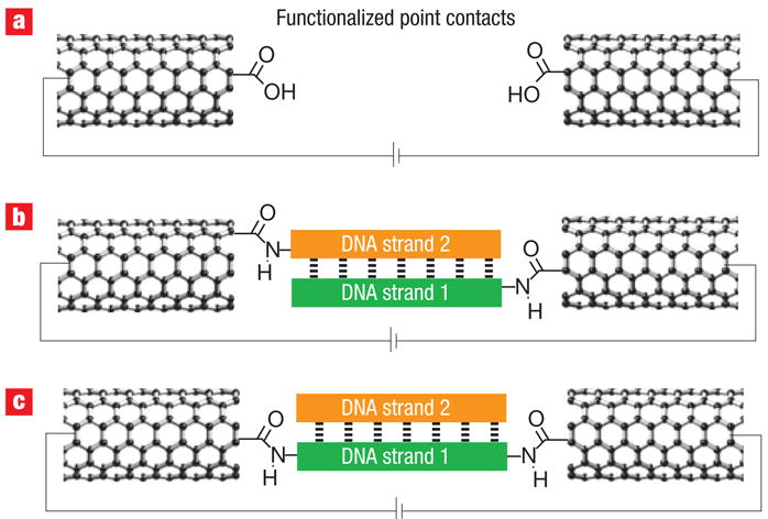
a, Functionalized point contacts made through the oxidative cutting of a SWNT wired into a device. b, Bridging by functionalization of both strands with amine functionality. c, Bridging by functionalization of one strand with amines on either end.
We reconnected the carbon nanotube gap with single DNA molecules terminated with amines using a two-step strategy. First, the freshly cut carbon nanotubes were immersed in a buffer solution containing standard amide coupling and activating agents (Sulfo-NHS, EDCI). Then, the activated carbon nanotube termini were reacted with amine-modified DNA to covalently bridge the gap with a single molecule. Given that the cross-sectional area of duplex DNA (~3 nm2) is comparable to that of the SWNTs grown here, it is unlikely that more than one DNA duplex can fit lengthwise within the gap. We explored two different methods to bridge these gaps. In one method (Fig. 1b), one end each of the two strands of the DNA duplex are bound to the SWNT electrodes. In a second method (Fig. 1c), a single strand is bound between the ends of the SWNT electrodes. The strategy in Fig. 1c is inherently more interesting because it allows for dehybridization/rehydridization with mismatched strands. The measurements were carried out under ambient conditions. (See Supplementary Information for experimental details on DNA synthesis, device reconnection and DNA dehybridization/rehybridization.)
Figure 2 shows representative I–V curves for these two different methods of DNA attachment. We could not determine any significant difference between the conductance measurements when using these two connection strategies. In Fig. 2a we used a DNA duplex functionalized on both strands with an amine at the 5′ end. In the other case (Fig. 2b), we used a DNA duplex containing a strand functionalized at both the 5′ and 3′ ends. The black curves show the source–drain current (ISD) as a function of the gate voltage (VG) at a constant source–drain bias of 50 mV for the pristine nanotube. Before cutting of the SWNT, the device in Fig. 2a is a hole transporting semiconducting device, and the one in Fig. 2b is a metallic device. After cutting and initial treatment of the gap with coupling agents, the devices show no measurable current (as indicated by the red curves). The green curves in Fig. 2a,b illustrate the conductance of the two devices after reconnection with the two amine-modified DNAs.
Figure 2. Device characteristics for individual SWNTs connected with DNA.

a,b, Source–drain current versus VG at a constant source –drain voltage (50 mV) before cutting (black curve: 1), after cutting (red curve: 2) and after connection with the DNA sequence shown (green curve: 3), for a semiconducting SWNT device (a) and a metallic SWNT device (b). Guanine, G; cytosine, C; adenine, A; thymine, T.
In both cases shown here, the reconnected carbon nanotube devices recover their original p-type semiconducting or metallic properties. Note that the gate voltage that can be applied to the reconnected devices is limited; device breakdown is observed for gate voltages greater than 6 V. Over time, at these higher gate biases, the DNA bridges became poorer and poorer conductors until, ultimately, the current levels are at the noise level of the measurement (see Supplementary Information, Figs S1 and S2). It is difficult to determine if this effect could be due to a hydration layer of water around the devices. Table 1 summarizes the device characteristics measured in the course of this study for the devices before cutting, after cutting and after reconnection with amine-terminated DNA sequences. (See Supplementary Information, Figs S1–S7, for experimental details of the electrical measurements.) Using this method we obtained 10 working devices out of 370 that were tested.
Table 1.
Summary of the resistance values obtained before cutting and after reconnection.
| Before cutting |
After reconnection |
||||
|---|---|---|---|---|---|
| Carbon nanotube type | Effective resistance* (MΩ) | DNA sequence | Type of linkage† | Effective resistance* (MΩ) | DNA conductance (e2/h) |
| Semiconducting | 0.65 | Well matched | 5′ amine | 2.5 | 1.4 × 10⁻² |
| Semiconducting | 1.3 | Well matched | 5′ amine | 2.8 | 1.7 × 10⁻² |
| Semiconducting | 0.90 | CA mismatch | 5′ amine | 18 | 1.5 × 10⁻³ |
| Semiconducting | 0.48 | Well matched | 5′ & 3′ amine | 3.3 | 9.2 × 10⁻³ |
| Metallic | 0.23 | Well matched | 5′ & 3′ amine | 0.5 | 8.6 × 10⁻² |
| Metallic | 0.23 | CA mismatch | 5′ & 3′ amine | 155.0 | 1.7 × 10⁻⁴ |
| Metallic | 0.23 | GT mismatch | 5′ & 3′ amine | 111.0 | 2.3 × 10⁻⁴ |
| Metallic | 0.20 | CA mismatch | 5′ & 3′ amine | 67 | 3.9 × 10⁻⁴ |
| Semiconducting | 0.24 | GT mismatch | 5′ & 3′ amine | 31 | 8.5 × 10⁻⁴ |
| Metallic | 0.52 | Well matched (Alu I) | 5′ & 3′ amine | 36 | 7.3 × 10⁻⁴ |
| Semiconducting | 1.5 | Single-stranded | 5′ & 3′ amine | 3.0 | 1.7 × 10⁻² |
Resistance values were calculated using a gate bias of −4 V and a source–drain bias of −50 mV.
The 5′ amine linkage corresponds to a –OCONH–(CH)3 –NH2 linker on the 5′ ends of both strands. The 3′ and 5′ amine linkage corresponds to a –Pi –(CH2)3 –NH2 linker on both the 3′ and 5′ ends of one strand. See Supplementary Information, Figs S2 and S3 for the sequences used.
Devices were also reconnected with mismatched DNA, as it has been shown in a variety of experiments that single-base mismatches dramatically attenuate CT. The DNA duplexes and mismatches explored here are shown in Fig. 3a. The mismatched devices were found to have higher resistance than corresponding devices reconnected with well-matched DNA. These results could not be compared quantitatively with those on the well-matched duplex, because different devices were fabricated to test the different duplexes. A device was therefore first reconnected with well-matched DNA duplexes functionalized with the amines on the 5′ and 3′ termini of one strand, and then the duplex was dehybridized using a 1:1 solution of formamide and deionized water at 30 °C and rehybridized with different complements (Fig. 3a–c).
Figure 3. Mismatches have a large effect on DNA conductance.

a, Replacing well-matched (WM) duplexes with CA and GT mismatches. b, Source–drain current versus VG at a constant source–drain voltage (50 mV) for a SWNT device taken through the sequence 1 through 6. The current levels for points 2, 3, 5 and 6 are ~300 times lower. c, Source–drain current at VG = −3 V at a constant source–drain voltage (50 mV) for the sequence 1 through 6.
Figure 3b shows the corresponding current–voltage curves for this sequence of experiments, and Fig. 3c shows the current at VG = −3 V for this sequence at a constant source drain bias of 50 mV. Rehybridization with the complement so as to generate a CA mismatch reduced the current significantly and yielded an increase in the on-state resistance of nearly 300-fold from 0.5 MΩ to 155 MΩ (Fig. 3c). Replacing the complement featuring a CA mismatch with a complement featuring a GT mismatch yielded no changes in the device characteristics. However, the original on-state resistance and nanoamp current levels could then be recovered by replacing the GT mismatched complement with the original well-matched sequence. Importantly, the device could be taken through multiple dehybridization/rehybridization cycles, as shown in Fig. 3b,c.
As further confirmation that CT in the carbon nanotube gap is DNA-mediated, we reconnected separate devices first with DNA featuring a GT mismatch or DNA featuring a CA mismatch (see Supplementary Information, Figs S3 and S4). Dehybridization of the mismatched DNA and replacement with well-matched DNA yielded an increase in the current and a decrease in the on-state resistance in both instances. It is important to note that the thermodynamically stable GT mismatch produced an effect that is identical to that found with the thermodynamically destabilizing CA mismatch. As we have found in solution experiments, the attenuation in DNA CT seen with mismatches does not correlate with thermodynamic stability of the duplex34. Ultrafast spectroscopic experiments indicate that DNA CT depends upon the sequence-dependent dynamics of DNA (ref. 35). Certainly, the changes observed here in the electrical characteristics of the device with mismatches cannot be due to poorer stability of the DNA.
Although the mismatch experiments provide strong evidence that the observed signals do not result from ionic conduction from the DNA molecules, as an additional control, newly cut devices were subjected to the same reconnection conditions but with the DNA excluded. After removal from the solution and rinsing, all of the devices treated in this manner remained at open circuit with no measurable current.
Devices were also reconnected with single-stranded DNA featuring amines at both the 5′ and 3′ ends but without its complement. Although carbon nanotube gaps could be bridged with the single-stranded DNA, the resulting devices were found to be highly unstable (see Supplementary Information, Fig. S5). After three voltage cycles, the current passing through single-stranded DNA degraded to open-circuit levels. Such instability may result from voltage-induced oxidation of the exposed nucleobases and was not observed with duplex DNA.
Additional control experiments were performed to determine if non-specific absorption of DNA could be responsible for the conduction changes during dehybridization/rehybridization. Devices were partially cut with a shorter oxygen plasma treatment before being taken through the sequential steps of reconnection and exchanges from matched to mismatched sequences. In essence, the SWNT is only nicked, not cut completely through, so the electrical connection is maintained. The devices treated in this way displayed little change in either the resistance or threshold voltage (see Supplementary Information, Fig. S6).
As a final test that the duplex DNA within the gap adopts a native conformation under the conditions of the experiment, we used Alu I, a blunt end restriction enzyme, to cut the DNA (Fig. 4). Alu I only cuts DNA that is in its native conformation. Devices were reconnected with duplex DNA containing the restriction sequence 5′-AGCT-3′. The device was subsequently incubated with Alu I, resulting in a concomitant decrease in the current to the noise limits of the measurement. As another control, a device reconnected with a nearly identical sequence that featured the sequence 5′-AGTC-3′ in place of the restriction site was incubated with Alu I. In this instance, no significant change was observed in the electrical characteristics of the device (see Supplementary Information, Fig. S7). These data support the observation of a sequence-specific restriction event. The enzyme is able to cleave its target sequence, yielding no detectable current in the device. Under the experimental conditions presented, then, the DNA duplex is intact, and the results suggest that it adopts a native conformation.
Figure 4. Enzymes can be used to cleave the DNA between the ends of the SWNTs.

Source–drain current versus VG at a constant source–drain voltage (50 mV) for a metallic SWNT device after cutting and reconnection with the shown DNA sequence before (green curve: 1) and after reaction with Alu 1 (red curve: 2).
We can now place the values found here in the proper context to establish a range for the conductivity of a single, intact DNA duplex. Our measurements place the resistance of well-matched DNA duplexes with ~6 nm length in the range of 0.1–5 MΩ (Table 1). For comparison, based on the bulk c-axis resistance, highly oriented pyrolytic graphite (HOPG) with similar dimensions should also have a resistance of ~1 MΩ (ref. 36). We estimate this value by substituting a HOPG stack of equivalent diameter for the double-stranded DNA. Thus it appears that DNA, in its well-matched and well-stacked duplex form, behaves electrically much like an array of stacked aromatic graphite planes. Importantly, just as we have seen in solution, the presence of intervening mismatches attenuates DNA-mediated CT. This attenuation leads to a ~300-fold increase in resistance. Such an increase in the resistance of mismatched DNA is consistent with previously reported STM measurements31–33. Also, it should be noted that even within our own measurements, the covalent σ-bonded linkages at the termini of the DNA duplex must also decrease the conductivity observed versus the conductivity expected with coupling directly into the base-pair stack. Therefore, the values obtained represent the upper limits of the resistance of the DNA π-stack.
In conclusion, we have outlined a method to integrate a single DNA duplex within an electrical device. The DNA molecules are covalently wired into electrical circuits through robust amide linkages that are stable over a wide range of chemistries and conditions. The experiments presented here illustrate the ability of DNA to mediate CT over significant distances and allow for the direct measurement of the resistance of a single well-matched DNA molecule. It is perhaps not surprising that DNA, if in its native conformation, and containing a stack of aromatic heterocycles in its core, resembles the aromatic stacked planes of graphite with respect to electrical characteristics. However, significantly, CT through a DNA assembly is sensitive to perturbations that arise in the base-pair stack. As illustrated directly here, as well as in solution experiments, single base mismatches attenuate CT through DNA. A molecular π-stacked array in solution is necessarily less robust than a solid-state conductive material. Thus, although the sensitivity of DNA CT to perturbations in stacking suggests that DNA may not be appropriate to serve as a robust wire for nanoelectronic circuits, DNA molecules bridging nanodevices can surely serve as uniquely powerful reporters to transduce biochemical events into electrical signals at the single-molecule level.
Supplementary Material
Acknowledgments
We acknowledge primary financial support from the Nanoscale Science and Engineering Initiative of the National Science Foundation (NSF) under NSF award number (CHE-0117752 and CHE-0641523) and by the New York State Office of Science, Technology, and Academic Research (NYSTAR) and the NSF NIRT Award (ECCS-0707748). C.N. acknowledges a NSF CAREER award (no. DMR-02-37860). J.K.B. thanks the National Institutes of Health (NIH) (JKB-GM61077) for their financial support of this work.
Footnotes
Supplementary information accompanies this paper on www.nature.com/naturenanotechnology.
Author contributions
X.G. and A.G. performed the experiments and wrote the manuscript. J.H., J.K.B. and C.N. designed the research and wrote the manuscript.
References
- 1.Eley DD, Spivey DI. Semiconductivity of organic substances: Nucleic acid in dry state. Trans Faraday Soc. 1962;58:411–415. [Google Scholar]
- 2.O’Neill MA, Barton JK. In: Sequence-Dependent DNA Dynamics: The Regulator of DNA-Mediated Charge Transport in Charge Transfer in DNA. Wagenknecht HA, editor. Springer-Verlag; Weinheim, Germany: 2005. pp. 27–75. [Google Scholar]
- 3.Schuster GB. Long-range charge transfer in DNA I & II. Top Curr Chem. 2004;236 [Google Scholar]
- 4.Giese B. Long-distance electron transfer through DNA. Ann Rev Biochem. 2002;71:51–70. doi: 10.1146/annurev.biochem.71.083101.134037. [DOI] [PubMed] [Google Scholar]
- 5.Delaney S, Barton JK. Long-range DNA charge transport. J Org Chem. 2003;68:6475–6483. doi: 10.1021/jo030095y. [DOI] [PubMed] [Google Scholar]
- 6.Murphy CJ, et al. Long-range photoinduced electron transfer through a DNA helix. Science. 1993;262:1025–1029. doi: 10.1126/science.7802858. [DOI] [PubMed] [Google Scholar]
- 7.Lewis FD, et al. Distance-dependent electron transfer in DNA hairpins. Science. 1997;277:673–676. doi: 10.1126/science.277.5326.673. [DOI] [PubMed] [Google Scholar]
- 8.Hall DB, Holmlin RE, Barton JK. Oxidative DNA damage through long-range electron transfer. Nature. 1996;382:731–735. doi: 10.1038/382731a0. [DOI] [PubMed] [Google Scholar]
- 9.Dandliker PJ, Holmlin RE, Barton JK. Oxidative thymine dimer repair in the DNA helix. Science. 1997;275:1465–1468. doi: 10.1126/science.275.5305.1465. [DOI] [PubMed] [Google Scholar]
- 10.Kelley SO, Barton JK. Electron transfer between bases in double helical DNA. Science. 1999;283:375–381. doi: 10.1126/science.283.5400.375. [DOI] [PubMed] [Google Scholar]
- 11.Gasper SM, Schuster GB. Photoinduced electron transfer to anthraquinones linked to duplex DNA: the effect of gaps and traps on long-range radical cation migration. J Am Chem Soc. 1997;119:12762–12771. [Google Scholar]
- 12.Giese B, Amaudrut J, Kohler AK, Spormann M, Wesselly S. Direct observation of hole transfer through DNA by hopping between adenine bases and by tunnelling. Nature. 2001;412:318–320. doi: 10.1038/35085542. [DOI] [PubMed] [Google Scholar]
- 13.Wan C, Fiebig T, Kelley SO, Treadway CR, Barton JK. Femtosecond dynamics of DNA-mediated electron transfer. Proc Natl Acad Sci USA. 1999;96:6014–6019. doi: 10.1073/pnas.96.11.6014. [DOI] [PMC free article] [PubMed] [Google Scholar]
- 14.Nunez ME, Hall DB, Barton JK. Long-range oxidative damage to DNA: Effects of distance and sequence. Chem Biol. 1999;6:85–97. doi: 10.1016/S1074-5521(99)80005-2. [DOI] [PubMed] [Google Scholar]
- 15.Henderson PT, Jones D, Hampikian G, Kan Y, Schuster GB. Long-distance charge transport in duplex DNA: The phonon-assisted polaron-like hopping mechanism. Proc Natl Acad Sci USA. 1999;96:8353–8358. doi: 10.1073/pnas.96.15.8353. [DOI] [PMC free article] [PubMed] [Google Scholar]
- 16.Kelley SO, Homlin RE, Stemp EDA, Barton JK. Photoinduced electron transfer in ethidium-modified DNA duplexes: Dependence on distance and base stacking. J Am Chem Soc. 1997;119:9861–9870. [Google Scholar]
- 17.Boal AK, et al. DNA-bound redox activity of DNA repair glycosylases containing [4Fe-4S] clusters. Biochemistry. 2005;44:8397–8407. doi: 10.1021/bi047494n. [DOI] [PubMed] [Google Scholar]
- 18.Nunez ME, Holmquist GP, Barton JK. Evidence for DNA charge transport in the nucleus. Biochemistry. 2001;40:12465–12471. doi: 10.1021/bi011560t. [DOI] [PubMed] [Google Scholar]
- 19.Boon EM, Salas JE, Barton JK. An electrical probe of DNA–protein interactions on DNA-modified surfaces. Nature Biotechnol. 2002;20:282–286. doi: 10.1038/nbt0302-282. [DOI] [PubMed] [Google Scholar]
- 20.Boon EM, et al. Mutation detection by electrocatalysis at DNA-modified electrodes. Nature Biotechnol. 2000;18:1096–1100. doi: 10.1038/80301. [DOI] [PubMed] [Google Scholar]
- 21.Guo X, et al. Covalently bridging gaps in single-walled carbon nanotubes with conducting molecules. Science. 2006;311:356–359. doi: 10.1126/science.1120986. [DOI] [PubMed] [Google Scholar]
- 22.Guo X, et al. Single-molecule devices as scaffolding for multicomponent nanostructure assembly. Nano Lett. 2007;7:1119–1122. doi: 10.1021/nl070245a. [DOI] [PubMed] [Google Scholar]
- 23.Guo X, et al. Chemoresponsive monolayer transistors. Proc Natl Acad Sci USA. 2006;103:11452–11456. doi: 10.1073/pnas.0601675103. [DOI] [PMC free article] [PubMed] [Google Scholar]
- 24.Whalley AC, Steigerwald ML, Guo X, Nuckolls C. Reversible switching in molecular electronic devices. J Am Chem Soc. 2007;129:12590–12591. doi: 10.1021/ja073127y. [DOI] [PubMed] [Google Scholar]
- 25.Fink HW, Schonenberger C. Electrical conduction through DNA molecules. Nature. 1999;398:407–410. doi: 10.1038/18855. [DOI] [PubMed] [Google Scholar]
- 26.Porath D, Bezryadin A, de Vries S, Dekker C. Direct measurement of electrical transport through DNA molecules. Nature. 2000;403:635–638. doi: 10.1038/35001029. [DOI] [PubMed] [Google Scholar]
- 27.Storm AJ, van Noort J, de Vries S, Dekker CS. Insulating behavior for DNA molecules between nanoelectrodes at the 100 nm length scale. Appl Phys Lett. 2001;79:3881–3883. [Google Scholar]
- 28.Kasumov AY, et al. Proximity-induced superconductivity in DNA. Science. 2000;291:280–282. doi: 10.1126/science.291.5502.280. [DOI] [PubMed] [Google Scholar]
- 29.Gohen H, Nogues C, Naaman R, Porath D. Direct measurement of electrical transport through single DNA molecules of complex sequence. Proc Natl Acad Sci USA. 2005;102:11589–11593. doi: 10.1073/pnas.0505272102. [DOI] [PMC free article] [PubMed] [Google Scholar]
- 30.van Zalinge H, et al. Variable-temperature measurements of the single-molecule conductance of double-stranded DNA. Angew Chem Int Edn. 2006;45:5499–5502. doi: 10.1002/anie.200601263. [DOI] [PubMed] [Google Scholar]
- 31.Hihath J, Xu B, Zhang P, Tao N. Study of single-nucleotide polymorphisms by means of electrical conductance measurements. Proc Natl Acad Sci USA. 2005;102:16979–16983. doi: 10.1073/pnas.0505175102. [DOI] [PMC free article] [PubMed] [Google Scholar]
- 32.Wierzbinski E, Arndt J, Hammond W, Slowinski K. In situ electrochemical distance tunneling spectroscopy of ds-DNA molecules. Langmuir. 2006;22:2426–2429. doi: 10.1021/la053224+. [DOI] [PMC free article] [PubMed] [Google Scholar]
- 33.Ceres DM, Barton JK. In situ scanning tunneling microscopy of DNA-modified gold surfaces: bias and mismatch dependence. J Am Chem Soc. 2003;125:14964–14965. doi: 10.1021/ja0384476. [DOI] [PubMed] [Google Scholar]
- 34.Bhattacharya PK, Barton JK. The influence of intervening mismatches on long-range guanine oxidation in DNA duplexes. J Am Chem Soc. 2001;123:8649–8656. doi: 10.1021/ja010996t. [DOI] [PubMed] [Google Scholar]
- 35.O’Neill MA, Becker HC, Wan C, Barton JK, Zewail AH. Ultrafast dynamics in DNA-mediated electron transfer: base gating and the role of temperature. Angew Chem Int Edn. 2003;42:5896–5900. doi: 10.1002/anie.200352831. [DOI] [PubMed] [Google Scholar]
- 36.Tsang DZ, Dresselhaus MS. The c-axis electrical conductivity of kish graphite. Carbon. 1976;14:43–46. [Google Scholar]
Associated Data
This section collects any data citations, data availability statements, or supplementary materials included in this article.