Abstract
We report here a novel approach called MEMS microflex interconnect (MMFI) technology for packaging a new generation of Bio-MEMS devices that involve movable microelectrodes implanted in brain tissue. MMFI addresses the need for (i) operating space for movable parts and (ii) flexible interconnects for mechanical isolation. We fabricated a thin polyimide substrate with embedded bond-pads, vias, and conducting traces for the interconnect with a backside dry etch, so that the flexible substrate can act as a thin-film cap for the MEMS package. A double gold stud bump rivet bonding mechanism was used to form electrical connections to the chip and also to provide a spacing of approximately 15–20 µm for the movable parts. The MMFI approach achieved a chip scale package (CSP) that is lightweight, biocompatible, having flexible interconnects, without an underfill. Reliability tests demonstrated minimal increases of 0.35 mΩ, 0.23 mΩ and 0.15 mΩ in mean contact resistances under high humidity, thermal cycling, and thermal shock conditions respectively. High temperature tests resulted in an increase in resistance of > 90 mΩ when aluminum bond pads were used, but an increase of ~ 4.2 mΩ with gold bond pads. The mean-time-to-failure (MTTF) was estimated to be at least one year under physiological conditions. We conclude that MMFI technology is a feasible and reliable approach for packaging and interconnecting Bio-MEMS devices.
Keywords: Bio-MEMS, polyimide, Microflex technology, Biomedical microdevices, neural prosthetic, brain implants
1. Introduction
Packaging and reliability remain a major challenge for microelectromechanical systems (MEMS). MEMS packaging can exceed 80% of the total cost of the overall MEMS device [1, 2]. The reason for the high cost is that there are no standard packaging technologies for MEMS devices when compared to normal IC chips. Each MEMS device is unique and may require application specific packaging challenges. Bio-MEMS devices have additional packaging challenges related to biocompatibility issues and operating conditions in the biological tissue or fluid [3, 4]. In this paper, we present a novel packaging and interconnect technology for a Bio-MEMS device with moveable parts extending off the edge of the chip.
There are two types of packaging approaches for MEMS devices, thin-film and cap bonded devices 5. Thin film caps are usually created during the fabrication process and offer many advantages. Since thin film packages are usually made during the fabrication of the MEMS device they have to be planned as part of the fabrication process, which increases the integration complexity [5]. MEMS devices that are fabricated and shipped as single devices to the users must use a cap bonded type of device.
There are multiple ways of bonding a cap onto a MEMS device that have been reported including anodic bonding of glass to silicon [6]. Thermocompression bonding of glass to silicon has also been shown [7]. The use of intermediate layers of solder, PSG (phosphosilicate glass) [8], glass frit bonding [9], and transient liquid phase [10] bonding have all been demonstrated recently. Localized heating bonding using polysilicon has also been used and has the advantage of controlling the temperature at the bond site [11]. Epoxy bonding [12, 13] has been used but has limited use since it is not hermetically sealed, which is often desired in most MEMS devices. Other low-temperature bonding techniques include the use of polymers like SU-8 [14], benzo-cyclobutene BCB [15], poly-dimethyl siloxane (PDMS) [16] and parylene-C [17–19].
The most common type of material used for the cap is glass, silicon, or metals like aluminum. Implantable MEMS devices have several necessary packaging requirements that are not needed in standard industrial MEMS devices including: (1) biocompatibility, (2) flexibility, (3) lightweight and small size, and (4) durability in the harsh tissue environment.
The novel Bio-MEMS device whose packaging needs are addressed in this study uses thermal microactuators to move polysilicon microelectrodes in the brain in order to record activity from single neurons [20]. The devices are fabricated using the SUMMiT-V process at Sandia National Laboratory which does not integrate packaging. The above devices are the first of a new generation of implantable prostheses using MEMS technologies in which the microelectrodes move and extend off the edge of the chip before they enter the brain tissue during implantation. Traditional hermetic packaging for implantable devices, are therefore inadequate for the above devices due to the movable microelectrodes that extend beyond the confines of the chip over a distance of several millimeters. Therefore, the first need in packaging for this new generation of implantable MEMS devices is operating room to enable successful movement of micromachined mechanical parts.
The second need is for flexible interconnects for the Bio-MEMS device. A flexible interconnect is needed for brain implants in order to mechanically isolate the interconnect from the chip so that forces (exerted during repeated insertion and removal of external recording devices over the life-time of the implant) do not transfer to the microelectrodes in the brain. Such mechanical forces transmitted to the brain implants are widely hypothesized to be one of the causes of failure in these implants. Mechanical forces on the microelectrode relative to the surrounding brain tissue could (a) exacerbate tissue injury responses leading to a failure of the tissue-microelectrode interface and/or (b) result in a relative micromotion of the microelectrode with respect to the surrounding brain tissue leading to a loss of electrical connectivity between the recording site of the microelectrode and the single neuron that it is recording from.
We propose a flexible polyimide cap and interconnect approach for packaging this device. The polyimide that was selected for the flexible circuit substrate (PI2611, HD Microsystems), is widely used in biomedical devices and proven to be biocompatible [21] with low water uptake (<0.5%), a low CTE that is comparable to Si3N4 (3 ppm/C°), and a high elastic modulus (8.5 GPa). Various non-MEMS based implantable devices have used polyimide or parylene based packages. Most of the devices use a flip-chip based package, however most flip-chip based packages require the need of an underfill or anisotropic conductive film [22, 23]. Meyer et al. developed a unique technique called microflex interconnect technology (MFI), using gold stud bumps to form rivet bonds [24]. Rivet bonds have previously been used in MEMS packaging [25]. We report here a modified version of the above packaging technology, which will be henceforth referred to as MEMS microflex interconnect technology (MMFI), for Bio-MEMS devices that have movable parts. MMFI uses a double stub bump approach to add space for the actuators to operate efficiently, and a backside etch of the polyimide in order to create a cap and micro-channels. The micro-channels allow the microelectrodes to extend and move with ease off the edge of the chip.
II. Moveable Microelectrodes for Neural Recording
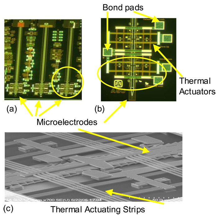
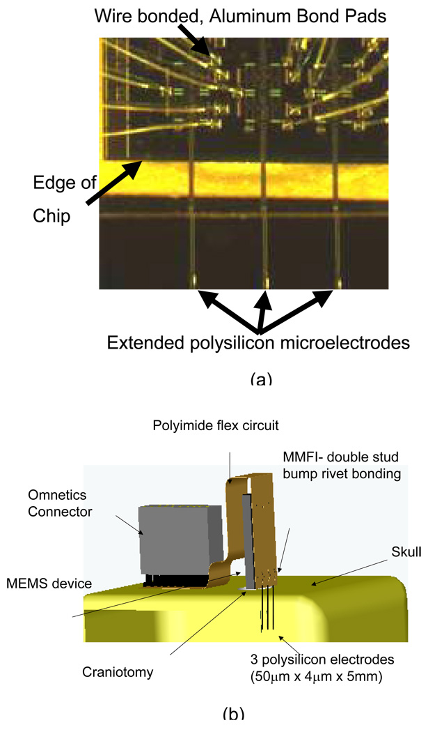
The Bio-MEMS devices used in this study were fabricated using the SUMMiT-V™ process at Sandia National Laboratories, Albuquerque, NM. Details of the device and fabrication process have been previously reported [20, 26] (Fig. 1). Electro-thermal V-beam actuators are used in the device to move microelectrodes off the edge of the chip and into the brain in order to monitor neuronal activity. The devices consist of three highly doped polysilicon microelectrodes (4 × 50 × 5000 µm). Movement of the microelectrodes was controlled by low-voltage square waveforms (8–10 V). Voltage is applied to the thermal actuators for 100–300 ms per step. The implanted microelectrodes do not get stimulated with the applied current or voltage due to nonconducting barriers between the thermal actuators and the microelectrodes. Typically the microelectrodes are moved at a rate of 0.5 Hz or 1 step every 2 seconds. However the rate can be easily modified. The microelectrodes move approximately 9 µm per step. A micrograph of the chip is shown in Fig. 2(a). The flexible interconnect and the chip will be encapsulated with a hydrophobic sealant to prevent fluid entry. During implantation the device was bonded using Poly(methyl methacrylate) PMMA to the skull of the animal in which the device was being implanted, and the extended microelectrodes penetrate the brain via a craniotomy as shown in Fig. 2(b). The flexible cap package is bonded to the skull and does not get implanted. Only the microelectrodes that extend off of the chip get implanted in the brain. The thermal actuators were used to reposition the microelectrodes post implantation in the event of a failure to record electrical activity from a single neuron or to seek electrical activity from single neurons in specific functional regions of the brain. Typically failures or loss of neuronal signals occur every couple of weeks or longer, and the microelectrodes need to move by few tens of microns on average in order to regain functional neuronal signals. Therefore, the total movement or activation of the actuators during operation is very small.
Figure 1.
Micrographs of thermal actuators (a) the front surface of the MEMS device showing all three microelectrodes and their microactuators (chip is 3mm wide and 6mm long) (b) close-up of the right microelectrode (50 µm wide) and the electro-thermal strips that move the microelectrodes (encircled) (c) SEM of the circled region of (b) showing the thermal actuators and the polysilicon microelectrode.
Figure 2.
(a) Micrograph of MEMS device for neural recording with microelectrodes extended off the edge of the chip. (b) Illustration of the MMFI design. The MEMS chip sits on the skull held in place by dental acrylic (not shown). The extended polysilicon electrodes penetrate the brain, after a craniotomy is performed, in order to record neuronal activity.
III. Fabrication of Flexible polyimide package and interconnect
The flexible polyimide substrate included metal traces, bond pads, holes for rivet bonding, a sidewall on the perimeter of the substrate, and micro-channels for the extended probes. The flexible circuit that is described below can also be used to package MEMS devices which do not have moving parts by disregarding the fabrication of the micro-channels. This would result in a more hermetically packaged device, which would still include a flexible cap and interconnection.
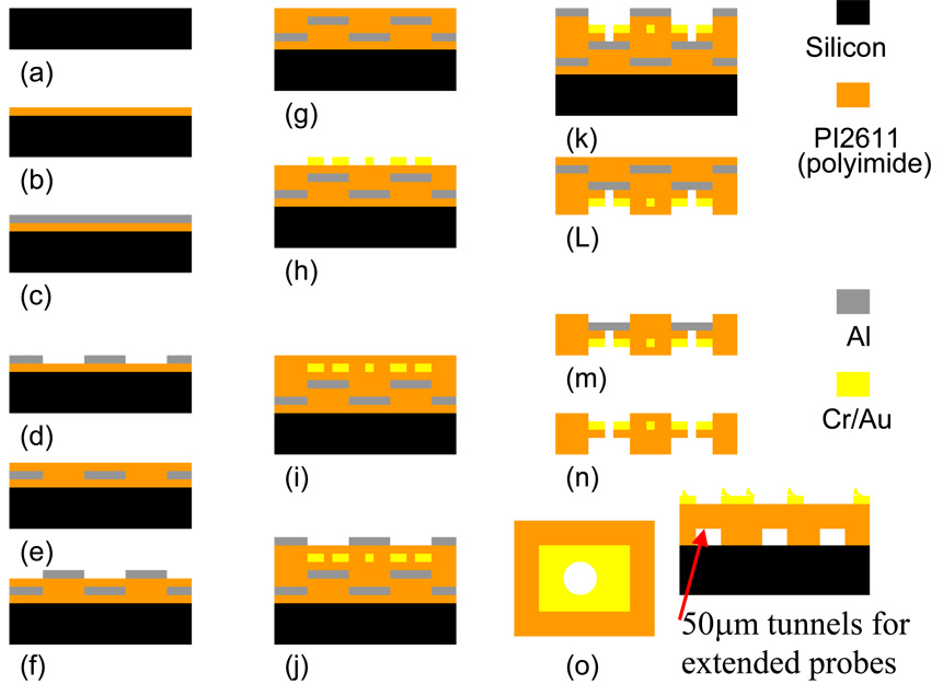
The first step in the process as illustrated in Fig. 3, was to perform a standard RCA clean of the silicon wafer, which acted as the support substrate throughout most of the process, in order to remove any organic contaminants (Fig. 3a). Then the silicon wafer underwent a dehydration step where it was placed in an oven (100°C–200°C) for 30 min. After letting the silicon wafer cool down to room temperature, a 4 µm thick layer of polyimide resin (Pyralin PI-2611, HD Microsystems) was spun onto the wafer. The polyimide was cured or imidized in an oven or hot plate with a ramp rate of 2–4°C/min starting at room temperature until the desired temperature of 350°C was achieved and held for 30 minutes (Fig. 3b). A micro-roughening and cleaning of the polyimide film was performed using reactive ion etch (RIE) before each metal deposition layer, in order to increase the adhesion of metal to polyimide. The RIE parameters for micro-roughening the surface were: (25 sccm O2, 150W, 100 m Torr). An aluminum layer (200 nm) was deposited (Fig. 3c) and structured with e-beam deposition and wet etching techniques to define the backside mask layer (Fig. 3d). A second polyimide layer of 15 µm, to achieve spacing between the cap and the moveable actuators, was spun and imidized as described above (Fig. 3e). A second aluminum layer (200 nm) forming the etch stop layer for both front and backside etching was deposited and structured by liftoff technique (Fig. 3f).
Figure 3.
Process for fabrication of thin flexible polyimide cap and interconnect circuit with patterned traces, vias, bond pads, and micro-channels.
A third polyimide layer of 8 µm was spun and imidized as described above, which acted as the bottom layer of the capped package (Fig. 3g). The third metallization layer (25 nm Cr, 350 nm Au) was deposited and patterned using thermal evaporation and wet-etching techniques (Fig. 3h). The gold layer serves as the interconnect traces and contact or bond pads. A fourth polyimide layer of 6 µm was spun and imidized as described above, which serves as the insulation layer for the traces (Fig. 3i). A fourth metallization layer (200 nm Al) was deposited and structured using wet etching techniques, which served as the hard mask for the front side etching (Fig. 3j).
Reactive ion etching was performed to open up the bond pads and create the hole or via in the polyimide, which was centered in the middle of the contact pads (Fig. 3k). The RIE parameters for etching through polyimide were: (25 sccm O2, 5 sccm CF4, 300W, 50 m Torr). The etch rate of polyimide using the parameters above was ~500 nm/min, with minimal sidewall effects (~80°). After this step, the polyimide film was mechanically removed from the supporting silicon wafer. The film was flipped upside down and placed on an aluminum plate using double-sided polyimide tape (Fig. 3l). Using the same RIE parameters described above a backside etch was performed in order to create the spacing for the moveable parts, and the micro-channels for the extended probes (Fig. 3m). The aluminum mask and stop layers were removed with an aluminum etchant (Type A, Transene Inc, Danvers, MA) (Fig. 3n). The devices were cleaned using IPA and DI water in order to remove any debris or residue. Like the MFI approach, a via was located in the center of the bond pads on the flexible circuit to facilitate mechanical and electrical connection with the MEMS device underneath. A 50 µm diameter via was made through the 100 × 100 µm gold bond pad on the polyimide film.
IV. MEMS MicroFlex Interconnection (MMFI) Technology
One of the key requirements for packaging the MEMS devices was to allow sufficient space for the actuators and other moving components to operate.
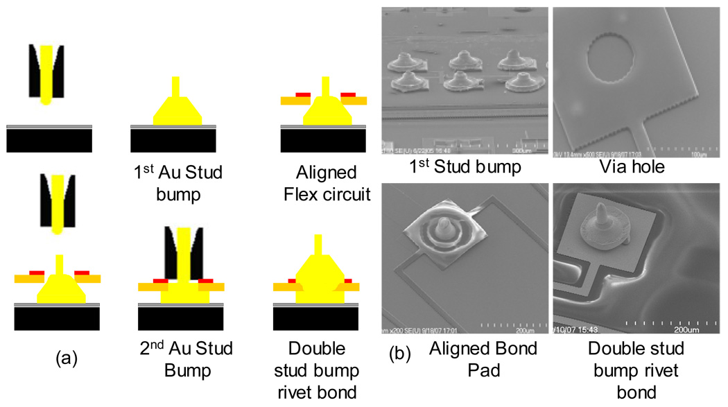
The first step in the MMFI process was to make gold stud bumps on the bond pads of the underlying MEMS device using a standard manual thermosonic ball bonder with 25 µm gold wire. The substrate was mounted on a holder and heated up to 150°C. The gold stud bumps were formed by making the first bond on the bond pad, then bringing the capillary straight up, and then brining it back down on top of the original bond. This technique gave the stud bump a high tail, which helps align the flexible polyimide circuit in the subsequent steps. Using this stud bump formation technique the average height of the stud bump was ~75 µm with a base height of around 25–35 µm, and a tail height around 30–50 µm. The MMFI technique does not require the heights of all the individual stud bumps to be consistent like in flip-chip technology. Once the gold stud bumps were formed, the MEMS device was cooled down to room temperature. Along the perimeter of the MEMS device a thin 100–200 µm wide layer of photoresist or epoxy was deposited using the Mikros pen dispensing unit (Ultra 2400, EFD Inc.). The photoresist or epoxy helped create an adhesive seal to prevent debris or fluid from entering the MEMS device, besides keeping the flexible circuit to be placed on top anchored down to the device and preventing dimpling in the flexible polyimide circuit. The micro-channel openings in the flexible substrate allowed for degassing of the cured epoxy. The via in the flex circuit was aligned and placed over the stud bumps on the MEMS device (step 3, Fig. 4). The added tail height of the stud bump helped align the flex circuit by acting as a pillar and preventing the flex circuit from moving once it was in place. The height of the gold stud bumps along with the added height of the sidewalls on the flexible circuit, allowed the flexible circuit to rest on the gold stud bump without encountering any of the moveable components.
Figure 4.
(a) Schematic illustration of MEMS Microflex interconnect (MMFI) technology using a double stud bump approach. (b) (upper left) SEM image of 6 single stud bumps on the MEMS device, (upper right) SEM image of an etched via through the gold bond pad and the flexible polyimide substrate, (lower left) SEM image of an aligned stud bump with tail extending out of the via in the flexible polyimide substrate, (lower right) an SEM image of a double stud bump bonded device.
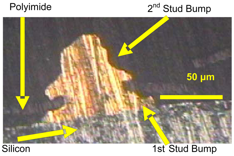
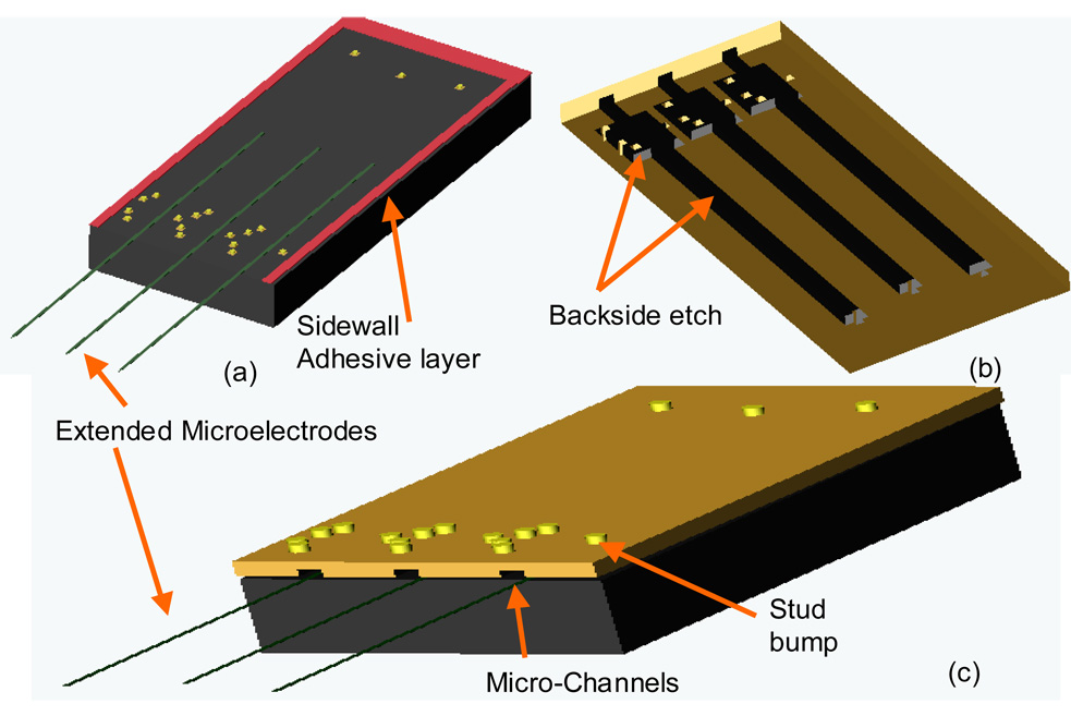
After the flex circuit was aligned, the device was mounted and heated to 120°C on the thermosonic bonder. The heat cured the photoresist or epoxy to create a seal between the flex circuit and the MEMS device, except in the front of the device where the microelectrodes would be extending off the edge of the MEMS device (no epoxy or photoresist is placed in the front edge of the MEMS device). A second gold stud bump was formed on top of the bond pad in the same manner as before (step 5, Fig. 4). The two-stud bumps formed a single rivet-bond. The second stud bump was also bonded with the contact pad on the flexible circuit. The force of the second stud bump reduced the height of the first stud bump underneath to around 15–25 µm. In Fig. 5, a micrograph of a cross-sectioned double rivet-bond using MMFI technology is shown. The cross section was made using standard metallurgic techniques. A schematic of the chip prior to bonding is shown in Fig. 6 (a), the flex circuit is shown in Fig. 6 (b), and the bonded device with micro-channels and extended microelectrodes is shown in figure 6(c).
Figure 5.
A cross section micrograph of a double stud-bump on the MEMS device using the MMFI approach. The first stud-bump rests on the bond pad on the MEMS device and the flexible polyimide sandwiched between the two gold stud bumps is seen as a faint horizontal line in the cross-sectional image.
Figure 6.
(a) A schematic of the MEMS chip with extended microelectrodes, gold stud bumps, and adhesive layer. (b) an angled schematic of the flexible package showing the sections that were backside etched (black) (c) shows a bonded MMFI device with micro-channels and extended microelectrodes. Schematics are not drawn to scale.
V. Reliability testing of MMFI
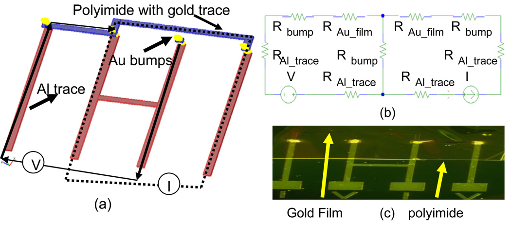
A test structure was designed and fabricated for investigating the electrical reliability of the double gold stud bump rivet bonds described above under four different test conditions as summarized in Table I. The custom “4-point probe” test patterns consisted of a bottom layer (test substrate) and a top layer of polyimide (Fig. 7a). The test patterns were modified from [23, 27, 28] in order to be used with MMFI. The test substrate was fabricated by depositing 1 µm thick aluminum on a silicon wafer with 1.2 µm Si3N4 deposited using PECVD. Aluminum was used as the bond pad material on the test substrate because of its wide use in IC packaging and because it was used in the bond pads in our MEMS device. The pattern was formed using standard photolithography techniques and wet etching the aluminum layer (Type A, Transene Inc, Danvers, MA). Another layer of photoresist was applied without patterning in order to act as a mask during the dicing process. Once the test substrate was diced, the photoresist was removed in hot (80°C) Microstrip and then cleaned using IPA and DI water. The test substrate consisted of four big bond pads (500 × 500 µm) that were evenly spaced by 200 µm and acted as the probed pads, along with four smaller pads (100 × 100 µm), which acted as the contact pads for gold stud bumps. The interconnect traces were 50 µm wide. The polyimide flexible circuit cap was fabricated as described above in section III. It consisted of four gold bond pads (100 × 100 µm) with a thickness of 250 nm. A hole or via (50 µm diameter) was created in the center of the bond pads using RIE as described above. The polyimide flexible circuit was then bonded to the test substrate using the MMFI approach described above (Fig. 7c).
Table 1.
Procedures for testing the reliability of the MMFI technique as adopted from MIL Standard 883.
| Humidity | 85°C / 85% relative humidity for 1000 hours |
| Temperature Cycling | 125°C to −40°C in air, 10 min dwell-time for 500 hours |
| Thermal Shock | 150°C to −80°C, 10s switch-time, 10 min dwell-time, 300 cycles |
| High Temperature | 300°C, 500 hours |
Figure 7.
(a) Illustration of a custom designed 4-point probe device test substrate and flex circuit used to measure contact resistance. (b) Equivalent electrical circuit model for measuring contact resistance Rbump=resistance of gold stud bump, RAl_trace=resistance of aluminum film on test substrate, RAu_film= resistance of gold film on top flex circuit. (c) A micrograph of a bonded 4-point probe test device.
The contact resistance of the samples was measured using the 4-point probe method (Fig. 7a). Custom-made stainless steel (200 µm diameter) probes were bonded onto a custom made PCB. Connectors were bonded using standard SMT in order to record voltage output. A micromanipulator was used to make contact with bond pads in order to prevent misalignment. A constant dc current (10 mA) was applied to the circuit while the voltage drop was recorded using a low-voltage data acquisition system (Tucker Davis Technologies Inc., Alachua, FL). The contact resistance of one MMFI bond was obtained using Ohm’s law. A schematic of the 4-point probe data testing setup is shown in Fig. 7(a). The electrical circuit model of the test devices is shown in Fig. 7(b).
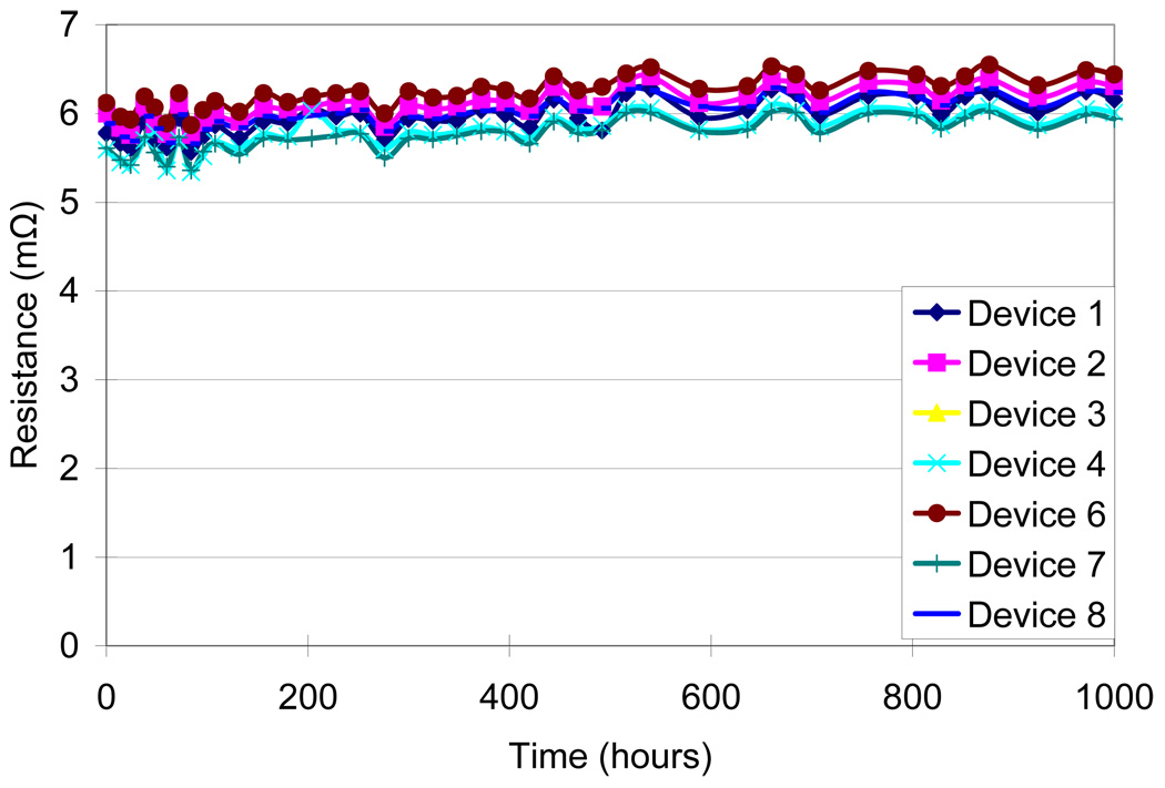
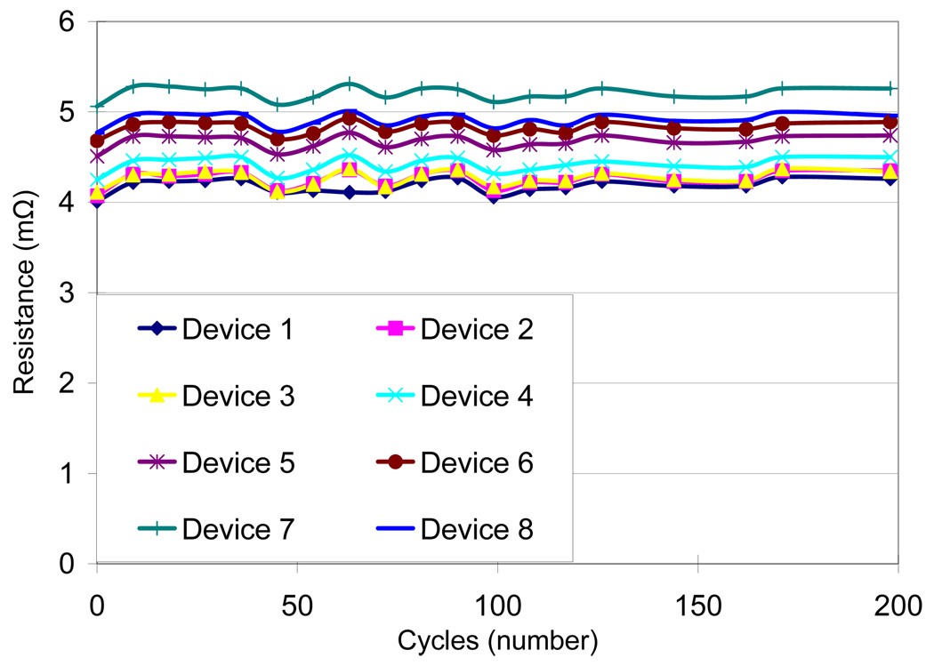
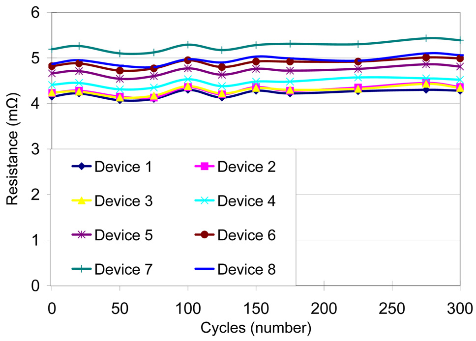
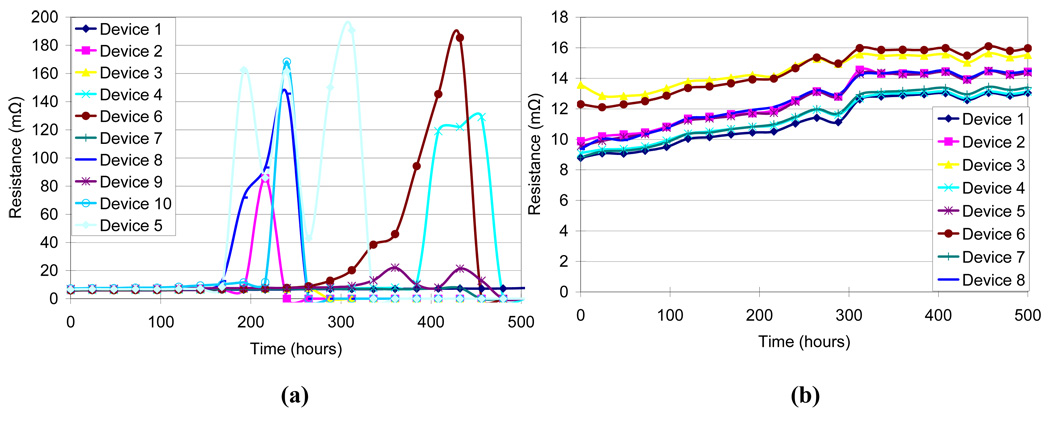
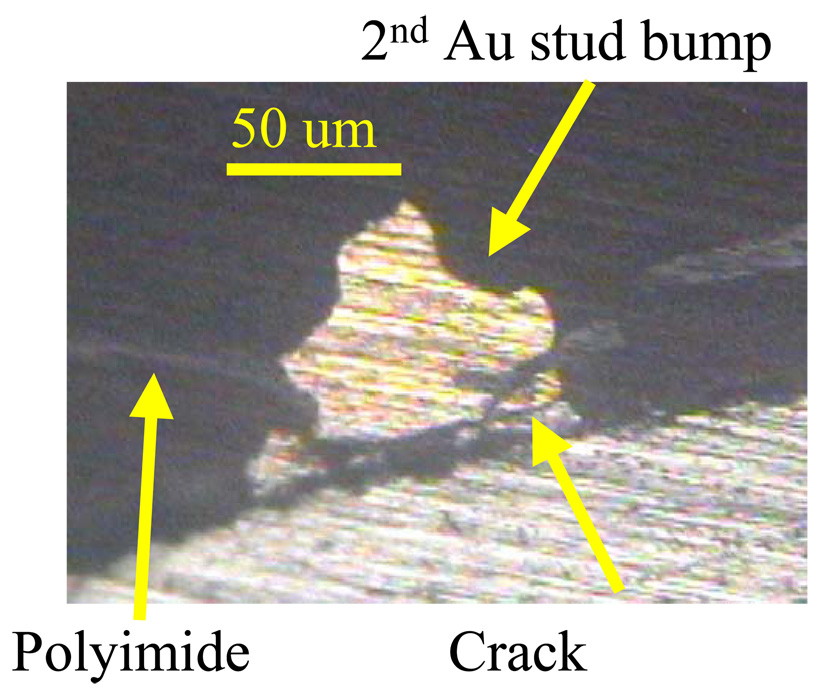
Four different test conditions were used to assess the reliability of the MMFI package according to MIL standard 883 (Table I). The contact resistance was measured before and after the testing procedure. Measurements were taken on several samples and average values were calculated. An accelerated high humidity test was performed for 1000 hours at 85% relative humidity and 85°C (SH-241 environmental chamber, Espec Inc.). Measurements were made every 24–48 hours. After 1000 hours of exposure there was a small increase in resistance from 5.84 ± 0.19 mΩ before exposure to 6.19 ± 0.17 mΩ after exposure (Fig. 8). A thermal cycling test between - 40°C and 125°C with 10-minute dwell-time was performed for 200 cycles or approximately 500 hours using the same environmental chamber. Measurements were made every 9–18 cycles. After 200 cycles there was a small increase in resistance from 4.43 ± 0.38 mΩ before exposure to 4.66 ± 0.35 mΩ after exposure (Fig. 9). A thermal shock test was performed using an oven (150°C) and a low temperature freezer (−80°C). The dwell-time was 10 minutes and the switching time was <15 seconds. The thermal shock test consisted of 300 cycles, with a measurement occurring every 25 cycles. A small increase in resistance was measured from 4.57 ± 0.37 mΩ before exposure to 4.72 ± 0.40 mΩ after exposure (Fig. 10). A high temperature test was performed using a high temperature oven (300°C) for 500 hours with measurements taken every 24 hours. Contact resistance increased significantly from 6.40 ± 0.45 mΩ before exposure to 94.87 ± 78.02 mΩ after exposure (Fig. 11a). Even a single bond failure creating an open circuit could result in the failure of the entire chain of stud bumps. Bond failures were seen in n=21 out of n=30 devices during the high temperature test. The failures were likely due to delamination caused from “Kirkendall’s” effect or “Horsting” voids, which are caused from the different diffusion rates between gold and aluminum under prolonged exposure to elevated temperatures [29–31]. A micrograph of a failed device at the aluminum-gold interface is shown in Fig. 12, which resembled failures seen due to Kirkendall or Horsting voids [32].
Figure 8.
Effects of 85% relative humidity and 85°C on the resistance of the MEMS Microflex interconnects over 1000 hrs.
Figure 9.
Resistance measurements of MEMS Microflex interconnects when exposed to temperature cycles ranging from 125°C to −40°C with 10 min dwell times for over 500 hrs corresponding to 200 cycles.
Figure 10.
Resistance measurements of MEMS Microflex interconnects when exposed to thermal shock treatment with temperature change from 150°C to −80°C with a transfer time of <15 seconds for 300 cycles.
Figure 11.
Resistance measurements of MEMS Microflex interconnects (MMFI) when exposed to high temperature (300°C) over 500 hours. (a) Effects of high temperature on MMFI using aluminum bond pads on silicon die. (b) Effects of high temperature on MMFI using gold bond pads on silicon die.
Figure 12.
A cross-sectioned micrograph of a failed bond after being exposed to high temperature (300°C) for a period of 500 hours.
In order to verify the cause of the failures and to develop a solution to the failures a new test substrate was fabricated using 250 nm gold in place of the aluminum test substrate. The flexible package and MMFI bonding approach were the same as described earlier. The high temperature test was repeated using the new gold test substrate at 300°C for 500 hours. A small increase in resistance was observed from 10.12 ± 1.67 mΩ before exposure to 14.29 ± 1.08 mΩ after exposure, however no failures were observed (Fig. 11b). Table 2 shows a summary of all of the contact resistance experiments performed.
Table 2.
Summary of resistance changes in the MMFI before and after exposure to the four different testing conditions.
| Test Conditions | Resistance (mean ± std.dev) mΩ | Increase in mean resistance (mΩ) | Number of Failures | |
|---|---|---|---|---|
| Before | After | |||
| Humidity (n=24) | 5.84 ± 0.19 | 6.19 ± 0.17 | 0.35 | 0 |
| Temperature Cycling (n=24) | 4.43 ± 0.38 | 4.66 ± 0.35 | 0.23 | 0 |
| Thermal Shock (n=24) | 4.57 ± 0.37 | 4.72 ±0.4 | 0.15 | 0 |
| High Temperature (Al trace) (n=30) | 6.4 ± 0.45 | 94.87 ± 78.02 | 88.47 | 21 |
| High Temperature (Au trace) (n=24) | 10.12 ± 1.67 | 14.29 ± 1.08 | 4.17 | 0 |
In order to determine the mean time to failure (MTTF) under physiological conditions we used a daisy chain configuration device (not shown) consisting of aluminum on Si test substrate and a matching polyimide flexible package bonded using MMFI technology. A 2-point probe test was used to measure resistance and check for failures resulting in an open circuit, which can be detected using a 2-point probe. One set of devices was placed in an environment of 85% relative humidity and 85°C while the other set of devices was placed in an environment of 20% relative humidity and 25°C. These two sets allowed us to calculate the empirical number (n) and the activation energy ΔEa in the Arrhenius equation shown below (eqn. 1) [33, 34], where RH is the relative humidity (85%, RH=85), k is the Boltzmann constant, T is the absolute temperature, and AF is the acceleration factor.
| (eqn. 1) |
Using eqn. 1 and the results from the above experiment, the lifetime of the device under any condition can be estimated. The MTTF under physiological conditions (37°C and 100% relative humidity) was estimated to be ~357 days assuming failures were observed today (168 days at 85% RH and 85°C). However, no failures have occurred to date, so this represents a lower bound limit, or the worst-case scenario. Table 3 shows the MTTF under both room conditions and physiological conditions using calculated n and ΔEa values (shown in column 3 of Table 3) and known tape-automated-bonding (TAB) values [35, 36] (shown in column 4 of Table 3). Using known TAB values of 3.0 of n and 0.9eV for ΔEa we calculated a MTTF of 33.2 years.
Table 3.
MTTF (Mean time to failure) results using the Arrhenius equation predict the MMFI will fail after 357 days in-vivo (worst-case scenario). No failures have occurred yet. MTTF estimated from standard TAB based Ea (activation energy) and n values is shown in column 4, and that from experimentally tested Ea and n values is shown in column 3.
| Test Enviroment | MTTF using experimentally calculated Ea (days) | MTTF using TAB value of Ea=0.9 (years) |
|---|---|---|
| Room Conditions (20C, 40% RH) | 581 | ~100 |
| in vivo (37C, 100% RH) | 357 | 33.2 |
VI. Discussion
We have addressed two critical needs in packaging for a new generation of Bio-MEMS devices that involve movable parts. The first need is for a flexible package and interconnect and the second need is for operating space within the package to enable movement of mechanical parts. We developed MEMS MicroFlex Interconnect (MMFI) technology that enabled us to assemble MEMS devices and SMT components on thin flexible polyimide substrate. The polyimide substrate acts as the bridge or cap package for the MEMS device, the interconnect, and circuit board for the connector. This integrated technology enabled us to reduce the size and weight of the device and compact all the levels of packaging into one single level. The interconnect densities created were 10 µm wide gold traces and 20 µm spacing. The small spacing is a requirement because of the small spacing in between bond pads on our MEMS device. Photolithography techniques can allow for smaller spacing or trace width if required. MMFI requires only two bonding processes and only one machine (wire bonder with ball bonding capabilities), which makes it feasible to be easily adopted by University labs or low-production prototyping companies. The flexible circuit is fabricated to create a bridge or cap wafer bond, and is sealed using epoxy bonding techniques. This procedure avoids having to screen-print bumps or perform flip-chip bonding using gold-to-gold bonding, which requires high temperature (>300°C) and high amounts of force (1–7 MPa) [37].
MIL standard 883 tests have shown that MMFI is a reliable and robust packaging technology. The MMFI reliability results in this paper are similar to the results of reliability tests on using MFI from previous results [24, 38], which showed no significant increase in resistance except under high temperature. MMFI failures occurred during the aluminum to gold interface in a few devices under high temperature conditions (300°C), which is likely caused by Kirkendall’s or Horsting voids as described earlier. However, this was eliminated with the use of gold bond pads on the test substrates, which created a gold-to-gold bond removing any intermetallic formation. Stieglitz et. al. showed a decrease in resistance when using gold-to-gold bonding, which they state is likely due to a healing process that reduces defects and leads to a more homogenous gold layer [38]. The MMFI results under high temperature resulted in an increase in resistance of 4.2 mΩ. The increase in resistance is likely caused by impurities or contamination of the gold through the wire bond, dicing process, and thermal evaporation process. Most Bio-MEMS devices operate at a temperature around 37°C, so failures due to intermetallic formations are unlikely under normal physiological conditions. The thermal actuators beams heat up to several hundred degrees Celsius, however, since the beams are small and conduction is quick structures only a few microns away get heated to only a few degrees Celsius [20]. Therefore, the heat caused from the actuators is not expected to have significant impact on the flexible polyimide package; however this will be carefully assessed in future studies. The voltage and current used to activate the actuators is not expected to have a major effect on the reliability, because of the small durations over which the actuators are expected to be activated over the lifetime of the device. Typically the microelectrodes will need to be moved a few hundred microns throughout the lifetime of the device, which corresponds to only a few seconds of applied voltage and current. In addition, the flexible polyimide interconnect will be sealed with a hydrophobic encapsulation that will prevent the entry of any fluids between the polyimide interconnect and the underlying MEMS chip. This will prevent any accidental hydrolysis of water that can happen with the voltages (8–10V) and currents used to activate the microactuators that are well outside the water window. Further, the non-conducting barriers in place between the actuators and the implanted microelectrodes that are in contact with brain fluids, will prevent any voltage or current applied for activating the actuators to be conducted by the microelectrodes.
Polyimide (PI-2611) was chosen for its low CTE (3ppm/°C), low water absorption (<0.5%), and high elastic modulus (8.5 GPa). There are several alternate materials that could also be used to fabricate the flexible circuit. Parylene-C is an attractive polymer that has several desirable features. It is deposited using chemical vapor deposition process at room temperature. Parylene-C is more conformal than spin coated polyimide. However, the glass transition temperature for parylene-C is much lower (~80–100°C), which means it cannot be used in high temperature processes. Since our devices require heating up to 200°C for a period of 30 minutes for subsequent processes to insulate the microelectrodes in the MEMS device, parylene-C could not be used in our production. Benzo-cyclobutene (BCB) is another material that is commonly used in bioimplantable devices. BCB like various polyimide materials has the attractive feature that it is photo-imageable and hence can be patterned readily. However, BCB was not chosen for our case because of the high CTE mismatch. Liquid Crystal Polymers (LCP) is another material that could be used to fabricate the flexible circuit, and is growing in popularity among the packaging developers [39–41].
The flexible circuit that is fabricated and bonded uses materials that are known to be biocompatible. Gold was chosen as the metal for the bond pads and interconnects, because of its biocompatibility, its ability to form mechanically and electrically stable bonds via gold-to-gold connection, and because it does not oxidize. However, other metals like copper could be used if the device is intended for non-implantable applications. Chrome is a corrosive metal, however no signs of corrosion have been seen throughout the testing. Cr/Au metal layers are common among implantable and in-vitro devices. However, if corrosion does occur with the use of chrome, titanium can be used instead of chrome as the adhesive layer. This technology could be used by other MEMS devices that need a thin film cap, which is post-packaged, flexible, and relatively easy to assemble. Currently this technique requires a skilled person to assemble the package since aligning of 50 µm features is done with tweezers and a microscope. An automated aligner is needed to enable mass production using this technology.
VII. Conclusion
A new technique, termed MEMS MicroFlex interconnect (MMFI) technology for interconnecting and packaging Bio-MEMS devices was developed. The MMFI technique was developed and applied to a moveable microelectrode device with polysilicon microelectrodes extending off the edge of the chip. The MMFI technology allows hybrid integration and assembly of bare silicon wafers (IC’s) and soldered components (SMD). The flexible circuit is directly bonded onto the MEMS device with a rivet double stud bump bond that interconnects through the via of the flexible circuit. Testing according to MIL standard 883 demonstrated that the MMFI technology is reliable and robust under normal physiological conditions. If a device is to be used in a high temperature environment exceeding a couple hundred degrees Celsius then gold-to-gold bonding should be formed to avoid failures at the aluminum to gold interface. Future work will be directed towards scaling-up the MMFI technology for developing a high-density cluster of MEMS devices for biomedical applications that require a large number of implanted microelectrodes.
We conclude that MMFI technology is well-suited for Bio-MEMS devices with or without moving parts. This novel interconnect technology is easy to assemble, since the only device that is required is a wire bonder with ball bonding capabilities. The ease of this technology will allow low-production prototyping and University Labs to create quick and easy packaging solutions for MEMS devices.
Acknowledgments
Research supported by grants R21NS051773 and R01NS055312 from the NIH and Arizona Biomedical Research Commission.
This work was funded by NIH grants R21NS051773 and R01NS055312 and the Arizona Biomedical Research Commission. The authors would like to thank Dr. Murat Okandan of Sandia National laboratories, Albuquerque, NM for help in fabricating the microactuated microelectrodes using the SUMMiTV™ process. The authors would also like to thank Nathan Bakken for his help with polishing the cross sectioned devices and the Center for Solid State Electronics Research (CSSER) at ASU for the use of their fabrication facilities.
References
- 1.Hsu T-R. Packaging Design of Microsystems and Meso-Scale Devices. IEEE Trans. Adv. Packag. 2000;vol. 23:596–601. [Google Scholar]
- 2.Malshe A, Brown W, Eaton W, Miller W. Challenges in the Packaging of MEMS. The Int. J. of Microcircuits and Electronic Packag. 1999;vol. 22:233–241. [Google Scholar]
- 3.Panchawagh H, Faheem F, Herrmann C, Serrell D, Finch D, Mahajan R. A flip-chip encapsulation method for packaging of MEMS actuators using surface micromachined polysilicon caps for BioMEMS applications. Sens. Actuators A, Phys. 2007;vol. 134:11–19. [Google Scholar]
- 4.Velten T, Ruf H, Barrow D, Aspragathos N, Lazarou P, Jung E, Malek C, Richter M, Kruckow J, Wackerle M. Packaging of Bio-MEMS: Strategies, Technologies, and Applications. IEEE Trans. Adv. Packag. 2005;vol. 28:533–546. [Google Scholar]
- 5.Stark B, Najafi K. A Low-Temperature Thin-Film Electroplated Metal Vacuum Package. J. Microelectromech. Syst. 2004;vol. 13:147–157. [Google Scholar]
- 6.Ziaie B, Von Arx J, Dokmeci M, Najafi K. A Hermetic Glass-Silicon Micropackage with High-Density On-Chip Feedthroughs for Sensors and Actuators. J. Microelectromech. Syst. 1996;vol. 5:166–179. [Google Scholar]
- 7.Cheng Y, Lin L, Najafi K. Localized Silicon Fusion and Eutectic Bonding for MEMS Fabrication and Packaging. J. Microelectromech. Syst. 2000;vol. 9:3–8. [Google Scholar]
- 8.Cheng Y, Lin L, Najafi K. Localized bonding with PSG or indium solder as intermediate layer. IEEE Int. Conf. on MEMS. 1999:285–289. [Google Scholar]
- 9.Sparks D, Massoud-Ansari S, Najafi K. Long-term evaluation of hermetically glass frit sealed silicon to Pyrex wafers with feedthroughs. J. Micromech. Microeng. 2005;vol. 15:1560–1564. [Google Scholar]
- 10.Welch W, Chae J, Najafi K. Transfer of Metal MEMS Packages Using a Wafer-Level Solder Transfer Technique. IEEE Trans. Adv. Packag. 2005;vol. 28:643–649. [Google Scholar]
- 11.Lin L. MEMS Post-Packaging by Localized Heating and Bonding. IEEE Trans. Adv. Packag. 2000;vol. 23:608–616. [Google Scholar]
- 12.Kim Y-K, Kim E-K, Kim S-W, Ju B-K. Low temperature epoxy bonding for wafer level MEMS packaging. Sens. Actuators A, Phys. 2008;vol. 143:323–328. [Google Scholar]
- 13.Van der Groen S, Rosmeulen M, Baert K, Jansen P, Deferm L. Substrate bonding techniques for CMOS processed wafers. J. Micromech. Microeng. 1997;vol. 7:108–110. [Google Scholar]
- 14.Pan C, Yang H, Shen S, Chou M, Chou H. A low-temperature wafer bonding technique using patternable materials. J. Micromech. Microeng. 2002;vol. 12:611–615. [Google Scholar]
- 15.Jourdain A, De Moor P, Baert K, De Wolf I, Tilmans H. Mechanical and electrical characterization of BCB as a bond and seal material for cavities housing (RF-) MEMS devices. J. Micromech. Microeng. 2005;vol. 15:S89–S96. [Google Scholar]
- 16.Satyanarayana S, Karnik R, Majumdar A. Stamp-and-Stick Room-Temperature Bonding technique for Microdevices. J. Microelectromech. Syst. 2005;vol. 14:392–399. [Google Scholar]
- 17.Kim H, Najafi K. Characterization of Low-Temperature Wafer Bonding Using Thin-Film Parylene. J. Microelectromech. Syst. 2005;vol. 14:1347–1355. [Google Scholar]
- 18.Kim H, Najafi K. Characterization of Aligned Wafer-Level Transfer of Thin and Flexible Parylene Membranes. J. Microelectromech. Syst. 2007;vol. 16:1386–1396. [Google Scholar]
- 19.Noh H-s, Moon K-s, Cannon A, Hesketh P, Wong CP. Wafer bonding using microwave heating of parylene intermediate layers. J. Micromech. Microeng. 2004;vol. 14:625–631. [Google Scholar]
- 20.Muthuswamy J, Okandan M, Gilletti A, Baker M, Jain T. An Array of Microactuated Microelectrodes for Monitoring Single-Neuronal Activity in Rodents. IEEE Trans. Biomed. Eng. 2005;vol. 52:1470–1477. doi: 10.1109/TBME.2005.851478. [DOI] [PMC free article] [PubMed] [Google Scholar]
- 21.Stieglitz T, Beutel H, Schuettler M, Meyer J-U. Micromachined, Polyimide-Based Devices for Flexible Neural Interfaces. Biomed. Microdevices. 2000;vol. 2:283–294. [Google Scholar]
- 22.Li C, Sauser F, Azizkhan R, Ahn C, Papautsky I. Polymer flip-chip bonding of pressure sensor on a flexible Kapton film for neonatal catheters. J. Micromech. Microeng. 2005;vol. 15:1729–1734. [Google Scholar]
- 23.Pai R, Walsh K. The viability of anisotropic conductive film as a flip chip interconnect technology for MEMS devices. J. Micromech. Microeng. 2005;vol. 15:1131–1139. [Google Scholar]
- 24.Meyer J-U, Stieglitz T, Scholz O, Haberer W, Beutel H. High Density Interconnects and Flexible Hybrid Assemblies for Active Biomedical Implants. IEEE Trans. Adv. Packag. 2001;vol. 24:366–374. [Google Scholar]
- 25.Shivkumar B, Kim C-J. Microrivets for MEMS Packaging: Concept, Fabrication, and Strength Testing. J. Microelectromech. Syst. 1997;vol. 6:217–225. [Google Scholar]
- 26.Jackson N, Stice P, Okandan M, Muthuswamy J. Long-term cortical recordings with Microactuated Microelectrodes. IEEE EMBS Conf. Neural Eng.; Kohala Coast, Hawaii. 2007. [Google Scholar]
- 27.Uddin M, Alam M, Chan Y, Chan H. Adhesion strength and contact resistance of flip chip on flex packages--effect of curing degree of anisotropic conductive film. Microelectron. Reliab. 2004;vol. 44:505–514. [Google Scholar]
- 28.Chan YC, Tan SC, Nelson S, Lui S, Tan CW. Electrical Characterization of NCP- and NCF-Bonded Fine-Pitch Flip-Chip-on-Flexible Packages. IEEE Trans. Adv. Packag. 2006;vol. 29:735–740. [Google Scholar]
- 29.Breach CD, Wulff F. New observations on intermetallic compound formation in gold ball bonds: general growth patterns and identification of two forms of Au4Al. Microelectron. Reliab. 2004;vol. 44:973–981. [Google Scholar]
- 30.Horsting CW. Purple Plague and Gold Purity. Reliab. Phys. Symp., 10th Annual; Las Vegas, NV. 1972. pp. 155–158. [Google Scholar]
- 31.Philofsky E, Hall E. A Review of the Limitations of Aluminum thin Films on Semiconductor Devices. IEEE Trans. Parts, Hybrids, and Packag. 1975;vol. 11:281–290. [Google Scholar]
- 32.Li M, Li S, Ji H. Metallurgical Behavior of Au/Al Bond Interface during High Temperature Storage of Ultrasonic Wedge Bonding. 7th Int. Conf. Electron. Packag. Tech.; Tokyo, Japan. 2006. [Google Scholar]
- 33.Dokmeci M, Von Arx J, Najafi K. Accelerated Testing of Anodically Bonded Glass-Silicon Packages in Salt Water. Int. Conf. Solid-State Sens. and Actuators. 1997 [Google Scholar]
- 34.Von Arx J, Ziaie B, Dokmeci M, Najafi K. Hermeticity Testing of Glass-Silicon Packages with on-chip Feedtrhoughs. The 8th Int. Conf. Solid-State Sens. and Actuators; Stockholm, Sweden. 1995. [Google Scholar]
- 35.Brown WD. Advanced Electronic Packaging. New York: 1999. [Google Scholar]
- 36.Chiao M, Lin L. Accelerated hermeticity testing of a glass-silicon package formed by rapid thermal processing aluminum-to-silicon nitride bonding. Sens. Actuators A, Phys. 2002;vol. 97–98:405–409. [Google Scholar]
- 37.Tsau C, Spearing M, Schmidt M. Fabrication of Wafer-Level Thermocompression Bonds. J. Microelectromech. Syst. 2002;vol. 11:641–647. [Google Scholar]
- 38.Stieglitz T, Beutel H, Meyer J-U. "Microflex"- A New Assembling Technique for Interconnects. J. Intel. Mat. Syst. Str. 2000;vol. 11:417–426. [Google Scholar]
- 39.Chen M, Pham A, Evers N, Kapusta C, Iannotti J, Kornrumpf W, Maciel J, Karabudak N. Design and Development of a Package Using LCP for RF/Microwave MEMS Switches. IEEE Trans. Microw. Theory. 2006;vol. 54:4009–4015. [Google Scholar]
- 40.Kingsley N, Bhattacharya S, Papapolymerou J. Moisture Lifetime Testing of RF MEMS Switches Packaged in Liquid Crystal Polymer. IEEE Trans. Compon. Packag. Tech. 2008;vol. 31:345–350. [Google Scholar]
- 41.Tentzeris M, Laskar J, Papapolymerou J, Pinel S, Palazzari V, Li R, DeJean G, Papageorgiou N, Thompson D, Bairavasubramanian R, Sarkar S, Lee J. 3-D-Integrated RF and Millimeter-Wave Functions and Modules Using Liquid Crystal Polymer System-on-Package Technology. IEEE Trans. Adv. Packag. 2004;vol. 27:332–340. [Google Scholar]


