Abstract
We explore the limits of a simple and facile process for transferring low aspect ratio, high resolution features defined by nanoimprint lithography. The process involves post-imprint deposition of an angle-evaporated hard mask. This widens the process window for residual resist removal and facilitates easy liftoff. An added benefit is a concomitant reduction of feature size. A post-lift-off annealing step produces high pattern uniformity and additional feature size reduction. The process is extremely robust and it enables relatively straightforward fabrication of sub-5 nm spherical structures. It is extendible to rectilinear patterns as well.
Nanoimprint lithography (NIL)1 is a high throughput patterning technique in which a pattern is formed in a thin polymer film that has been cast on a substrate by molding it to a relief image in a rigid template (mask). This is typically done under high pressure conditions at a temperature above the glass transition of the polymer. Depending upon the polymer (thermoplastic or UV-curable), the image may be set either by cooling the polymer until it solidifies (thermal imprint) or by crosslinking it using ultraviolet radiation, (UV imprint, 2,3 requiring a transparent template or substrate). Although there is no theoretical limitation for the resolution of the pattern imprinted by NIL,4 and the practical limitation is determined by the size of the features on the NIL template, pattern transfer from imprinted resist to substrate by metallization and lift-off can be challenging, particularly for patterns containing sub-20 nm features. This is especially true when thin resists are used. Thin resists are generally desirable for replication of very small features (thick resists require high aspect ratio structures on the template which are prone to failure due to sheer force during template/substrate separation). In addition, as the resist thickness is reduced, increasingly tighter control is required during removal of the residual resist layer from the bottom of the imprinted structures. Residual resist removal usually results in the overall reduction of the resist thickness, as well as in a widening of the imprinted structures, since perfectly anisotropic etching of polymers is not always easily achieved. Various methods, all of them based on applying double- or multi-layer resist systems (top-imaging and bottom-undercut layers) are generally used to deal with these challenges. Examples of such systems include the use of a thermo-printable resist on top of a PMGI layer, which is removed after the imprint by wet processing,5 or use of an imaging layer of photocurable resist (usually resistant to oxygen plasma etching) on top of an organic layer which is later removed by oxygen plasma,6 with an optional hard mask layer between the imaging and undercut layers.7 Even though line gratings with sub-20 nm half pitch have been successfully fabricated with such a double layer method,8 a reliable and robust process for making arrays of circular features or dots in the same fashion has not been demonstrated so far for feature sizes less than 35 nm. 9
In our work we fabricate moderately large area (200 μm × 200 μm) arrays of AuPd dots for the study of cytoskeletal protein binding interactions, where the biofunctionalized dots serve as recognition sites for cells transmembrane proteins.10 This work requires that these dots be the same size as the biomolecules being probed - usually less than 10 nm. The dots must also be arranged in arrays with various heterogeneous geometries.11 We have recently developed a new process in which nanoimprint lithography is combined with an angle-evaporated hard mask for fabricating arrays of dots with sub-10 nm diameter by lift-off.10 The process flow is shown schematically in Fig. 1. After NIL, a thin metal film is deposited by electron beam evaporation on the imprinted resist, while the substrate is held at an angle relative to the metal vapor flux. A large distance (about 1 m in our case) between the substrate and the metal source ensures that the metal vapor flux is essentially normal to the substrate. An appropriate tilt angle ensures that the metal deposition occurs only on the top of the resist and on the upper portion of the sidewalls of the imprinted openings that are exposed to the flux. Uniform sidewall deposition can be achieved by rotation of the substrate during evaporation. The deposited metal on the sidewalls will ‘squeeze” the dimensions of the features in the pattern. Increasing the metal thickness will further reduce the openings, ultimately leading to their complete closing. The residual imprinted layer is then etched in an oxygen plasma, with the angle-evaporated metal film as an etch mask. Finally, a second metal film is evaporated through this hard mask, followed by lift-off, which is easy and robust due to the undercut formed under the hard mask by the oxygen plasma. In this paper we present a detailed study of this process, exploring the limits of miniaturization achievable by this approach.
Figure 1.
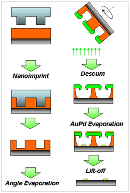
Schematic process flow of fabrication of an array of nanodots on a surface by nanoimprint in combination with angle evaporated metal mask.
The NIL templates in this work were formed from diamond-like carbon (DLC), which has been recently been shown to be a promising template material, possessing outstanding mechanical properties and easy processability. 12 The DLC films, 100 nm thick, grown on silicon substrate, were patterned by electron beam lithography using hydrogen silsesquioxane (HSQ, Fox-12, Dow Chemicals) as a resist.13 A 20 nm film of HSQ diluted in MIBK was spun on top of the DLC, exposed by e-beam lithography (FEI XL 30 Sirion with a Nabity NPGS pattern generator) without pre-baking in order to achieve high contrast,14 and developed in TMAH (LDD 26W, R&H Electronic Materials). The pattern consisted of arrays of single-pixel dots, with a horizontal spacing of 100 nm and a vertical spacing of 200 nm. The pattern was repeated several times with a range of exposure doses (from 11 to 18 fC/point), resulting in 20 nm-tall HSQ pillars with diameters ~ 10 – 35 nm. The pattern was transferred into the DLC by O2 RIE (Oxford PlasmaLab 80, RF power of 150 W, 30mTorr) to a depth of 30 nm, followed by stripping of the HSQ mask in a buffered HF solution (Fig. 2). Finally, an anti-adhesion fluorocarbon plasma treatment process was applied to the DLC template (Oxford PlasmaLab 80, C4F8, 88mtorr, 100W, 30s), to ensure clean separation of the template from the imprinted resist.15
Figure 2.
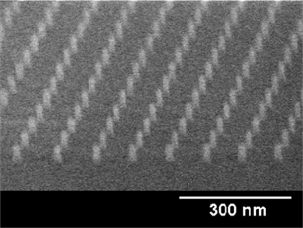
Side view SEM of nanoimprint mold which consists of arrays of pillars etched in DLC through an HSQ mask. The height of the pillars is about 30nm and their diameter varies from ~10nm to ~37nm, depending on the applied electron dose.
Thermal NIL was done using a 60 nm-thick film of PMMA (MW = 35K) as the imprint resist. NIL conditions were: a temperature of 180°C, pressure of 500 psi and imprint time of 5 minutes using a Nanonex BX200 imprinter.
Ti hard masks of 10, 20, 30 and 40 nm thickness were evaporated (Semicore SC2000, 0.01nm/s) on imprinted substrates, with the substrates tilted at 30 degrees under continuous rotation. Ti is easily deposited by electron beam evaporation, and it possesses excellent adhesion properties to various substrate materials; these were among the reasons for the selection of Ti as a hard masking material. It is also important to maintain a minimal grain size of the deposited metal in order to ensure complete conformal coverage of the coated surface and high quality transfer of the imprinted pattern to the metal mask. The strong gettering properties of Ti generally cause a significant drop in chamber pressure, aiding in the reduction of the metal film grain size, which can be as small as a few nm. 16 AuPd and SiO2 were tested as alternatives to Ti, but showed either increased edge roughness at the imprinted openings or complete closure of the openings.
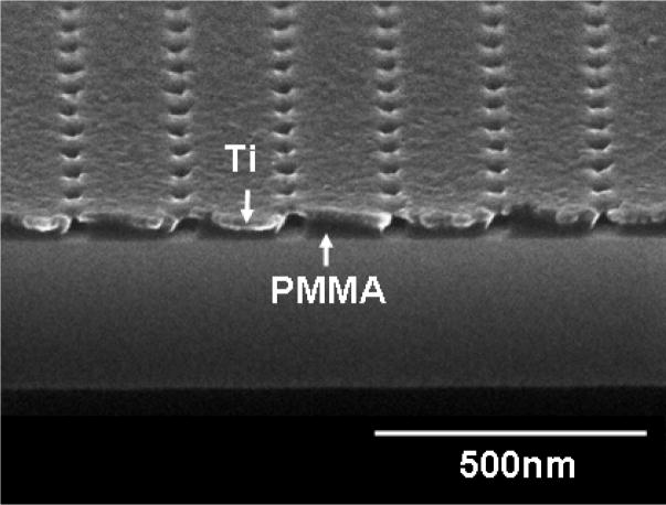
The residual resist was removed by etching in an oxygen plasma asher (Technics 800, 200mTorr, 50 W, 30s). Figure 3 shows a cross-sectional SEM image of a patterned substrate directly after the etching of residual PMMA from the bottom of the imprinted dots. 3 nm of AuPd with 1 nm of a Ti adhesion layer was deposited by e-beam evaporation after the residual resist etch, and the lift-off was done by immersion in boiling acetone for a few minutes.
Figure 3.
Cross sectional SEM of imprinted PMMA with angle-evaporated Ti mask after descum. The nearly complete removal of PMMA from the patterned areas and the resultant undercut are clearly seen in the image.
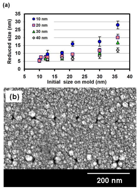
We measured the reduction in the size of the dots upon deposition of the Ti mask by scanning electron microscopy (Hitachi 4700). The imprinted resist openings were measured, as well as the size of the openings after Ti deposition (but before the descum step), in addition to the AuPd dots after liftoff. Figure 4a shows the diameter of the opening in the Ti mask vs. initial dimensions as defined by the template. The expected diameter reduction with every 10 nm of Ti is approximately (10 nm/π)×2 = 6.4 nm, taking into account the radial distribution of the evaporated metal over the openings. This reduction factor is faithfully reproduced in the experimental data for dots with larger diameters and for smaller values of the Ti mask thickness. For thicker Ti masks and smaller initial dots, the size reduction does not scale linearly with the Ti mask thickness. This is primarily due to the grain size of the deposited Ti film, which increases with increasing thickness,17 resulting in increased line edge roughness (LER) in the mask openings. The relative impact of the LER is greater for the smaller dots, where the Ti grain size approaches the dimensions of the dots themselves (Fig. 4b). The openings in the Ti mask could be clearly seen for almost every combination of initial dots size and Ti mask thickness. However, we observed a high density of defects (missing dots) after liftoff for arrays with dots smaller than 10 – 15 nm on which 30 40 nm-thick Ti was deposited. This was probably due to complete closure of the imprinted structures in these cases.
Figure 4.
(a) Reduction of dot size as a function of initial size as defined in NIL mold, for different thicknesses of the Ti mask. (b) 30nm Ti mask on the array of dots with an initial size of 12nm. The grain size of deposited Ti is of the same order of magnitude as the dots themselves.
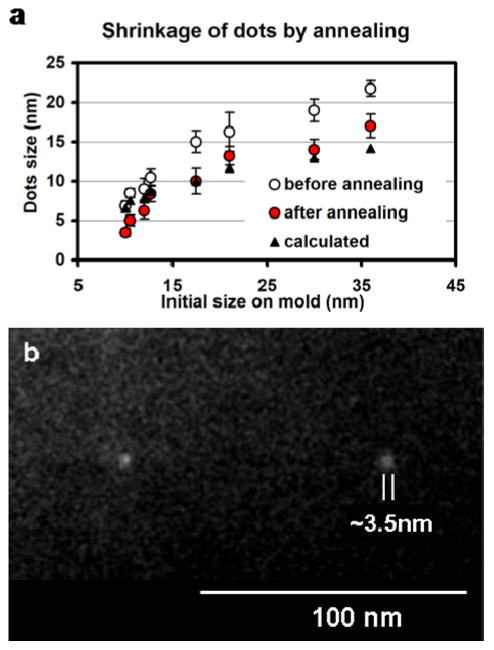
After liftoff, the dots are generally not perfectly round (Fig. 5a). This too can be attributed to the granular structure of the Ti hard mask, as well as to the granular structure of deposited AuPd. However, this can be addressed by thermal treatment.18 Annealing at 450 °C in nitrogen for 1 hour resulted in both a highly uniform shape well as a reduction in the diameter of the dots (Fig. 5b and 5c). Figure 6a shows the average dot size before and after the annealing vs. the initial size on the template for the case of a 10 nm Ti mask. The smallest dot size in this set was found to be about 7 nm in diameter after lift-off, and was further reduced to ~3.5 nm after annealing (Fig. 6b). Tapping mode AFM analysis (DI multimode IIIA) was used to study the change in the height of the dots upon the annealing (Fig. 7). The height of 15 nm diameter unannealed dots was 4.5 nm, in good agreement with the thickness of the deposited metal, as measured during deposition by a quartz crystal microbalance. After annealing, both the height and diameter were 9 nm, consistent with the notion that the annealing causes the dots to melt, resulting in approximately spherical structures upon solidification. This is reasonable, since the melting point for nanoscale particles is depressed from the bulk melting point.19 We found that for dots whose initial diameter was larger than ~ 14 nm, the total dot volume was unchanged after the annealing (Fig. 6a). However, for smaller dots, the annealed spheres were somewhat smaller than expected, indicating that some evaporation had taken place.20
Figure 5.
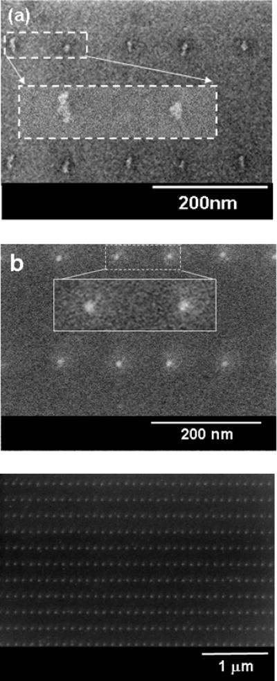
(a) AuPd dots before annealing. The dots correspond to an initial size of the mold pillars of ~18nm, and angle-evaporated Ti mask of 10 nm thickness. (b) The same dots after annealing. (c) Large area view of an array of annealed dots. An apparent “halo” around the nanodots is often seen on such images. This is probably due to charging of the substrate by the oxygen plasma, which is used to remove the residual PMMA film from these areas.
Figure 6.
(a) AuPd size reduction upon annealing at 450°C. The calculated values correspond to the diameter of perfectly spherical dots assuming no change in the material volume per dot upon the annealing. (b) SEM of ~3.5 nm dots, obtained after annealing.
Figure 7.
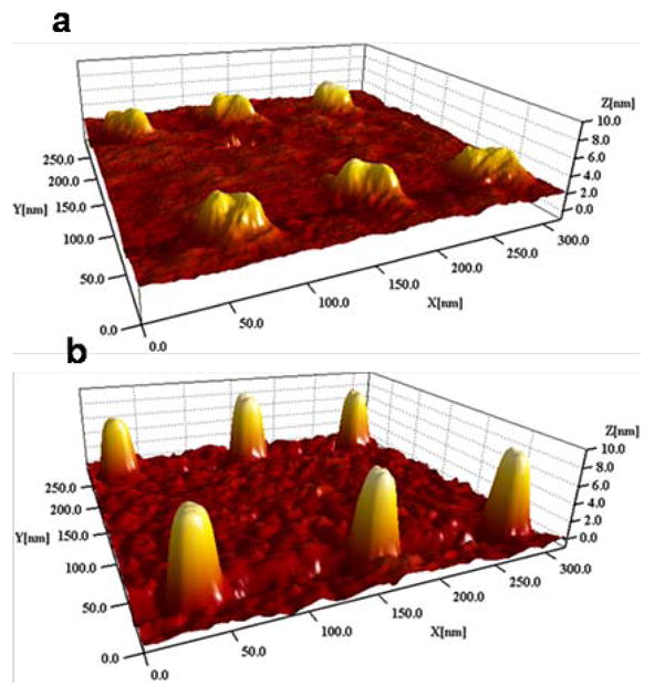
(a) AFM image of dots (15 nm lateral size) before annealing. The heigh is 4.5nm, which corresponds to the deposited Ti/AuPd. (b) Same dots after annealing. The height is 9nm, matching the new lateral dimensions.
The primary limitation factor in the size reduction of the imprinted features by an angle evaporated mask appears to be the increase in the grain size of the masking metal when its thickness is increased.17 Thus, it will be probably very difficult to reduce dots of ~30–40 nm dimensions to below 10 nm by an angle evaporated mask, since the large metal grains will cause pattern distortion on the same size scale as the features themselves. Instead, the initial features cannot be much larger than the target dimensions, so that the angle evaporated mask must not be thicker than 20–30 nm.
The final size of the metal dots after annealing can be controlled not only by the dot size after the liftoff, but also by the thickness of the final deposited metal 18 (AuPd in our case). In principle, reducing the thickness of the deposited metal should result in a reduction of the size of the final annealed structures. We found, however, that when a 0.5nm Ti/0.8nm AuPd film was used, the annealing did not result in a single particle, but rather in multiple nanoparticles with random sizes in the original dot areas (Fig. S1a). This result is consistent with previously reported results, where annealing of ultrathin (2 nm) metal and semiconductor patterned features 18,21 resulted in the formation of multiple particles. We believe that at these very low thicknesses, i.e., below the minimum required to form a continuous film, individual islands agglomerate. This can be remedied by annealing at a higher temperature, which imparts sufficient energy for diffusion over a range of up to a few tens of nm.22 We found that increasing the annealing temperature of our AuPd dots to 800 °C indeed resulted in the formation of a single dot at each site, with a smaller diameter than dots annealed at 450 °C. (Some of this size reduction can be attributed to evaporation.) The higher temperature anneal also results in some loss of positional control, as we observed migration of the dots of up to 20 nm from their original positions (Fig. S1b).
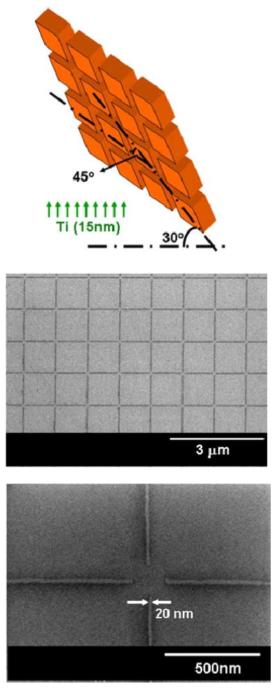
Our self-aligned pattern transfer technique is not restricted to dots. It can be used with rectilinear patterns as well. In this case, the substrate orientation in the evaporator must be fixed (as opposed to rotating), in order to maintain a constant shadowing angle for the lines.23 It is even possible to form a crossed X–Y grating, if the sample is held at a 45° angle relative to the grid axes (Fig. 8a). [For this we used an oxidized silicon nanoimprint template, with the template features etched to a depth of 30 nm (an anti-adhesion coating was applied using a commercial mold-release agent (Nanonex, NXT-100)).] The pattern consisted of orthogonal lines with widths in the range ~ 20 – 60 nm, separated by 1 μm in each direction.
Figure 8.
(a) Schematic of the orientation of substrate imprinted with a grid pattern during the metal mask evaporation. (b) and (c) The grid pattern after liftoff.
There were small openings at the vertices ranging from 0 – 200 nm. The imprint was done under the same conditions as described above, and 15 nm of Ti was deposited as a hard mask. Residual resist removal and Ti/AuPd deposition (1nm/3nm) were followed by lift-off, resulting in the grid shown in Fig. 8c.
Angle evaporated metal masking on nanoiprinted resist films provides simple and elegant way to transfer the pattern by metallization and liftoff, especially in the sub-20 nm size regime. This process creates an undercut beneath the metal mask, which assists the penetration of the solvent to the resist film during the liftoff process, making the liftoff itself very efficient (usually taking only a few minutes in boiling acetone) and clean. Due to the durability of the metal mask to oxygen plasma, the descum process used to remove the residual resist after imprint can be done within a relatively wide process window and a high tolerance. In addition, etch bias effects are completely eliminated. This process also alleviates the need for high aspect ratio 3D structures on the NIL template. In fact this aspect ratio can be as small as 1:1 – which is large enough to prevent the deposition of the masking metal at the bottom of the imprinted structures (a function of the evaporation angle). This can certainly contribute to template longevity, and it can simplify its fabrication process. The reduction in feature dimensions during the mask deposition is an added benefit of our approach, especially when there is need to produce features by liftoff at sizes below the resolution limits of the lithographic process used for template patterning. Controlled thermal treatment of the patterned metal structures enables access to the sub-5 nm regime, which is generally quite difficult. Angle evaporation masking in combination with NIL can be applied not only for dots arrays, but also for arrays of lines and even grids. In this case precise orientation of the imprinted substrate during the mask evaporation is required.
Supplementary Material
Acknowledgments
This work was supported by the Office of Naval Research under Award Number N00014-09-01-0250, as well as the National Institutes of Health through the NIH Roadmap for Medical Research under award number PN2EY016586 and by the National Science Foundation under award number NSF EF-05-07086. Additional support from the Nanoscale Science and Engineering Initiative of the National Science Foundation under NSF Award Number CHE-0641523 and from the New York State Office of Science, Technology, and Academic Research (NYSTAR) is also gratefully acknowledged.
References
- 1.Chou SY, Krauss PR, Renstrom PJ. Applied Physics Letters. 1995;67(21):3114–3116. [Google Scholar]
- 2.Ruchhoeft P, Colburn M, Choi B, Nounu H, Johnson S, Bailey T, Damle S, Stewart M, Ekerdt J, Sreenivasan SV, Wolfe JC, Willson CGIn. Patterning curved surfaces: Template generation by ion beam proximity lithography and relief transfer by step and flash imprint lithography. Marco Island, FL, USA, 1999; AIP for American Vacuum Soc; Marco Island, FL, USA: 1999. pp. 2965–9. [Google Scholar]
- 3.Stewart MD, Johnson SC, Sreenivasan SV, Resnick DJ, Willson CG. Journal of Microlithography Microfabrication and Microsystems. 2005;4(1):011002. [Google Scholar]
- 4.Hua F, Sun Y, Gaur A, Meitl MA, Bilhaut L, Rotkina L, Wang J, Geil P, Shim M, Rogers JA, Shim A. Nano Letters. 2004;4:2467. [Google Scholar]
- 5.Carlberg P, Graczyk M, Sarwe E-L, Maximov I, Beck M, Montelius L. Microelectron Eng. 2003:67–68. 203. [Google Scholar]
- 6.Tao J, Chen Y, Zhao X, Malik A, Cui Z. Microelectron Eng. 2005:78–79. 665. [Google Scholar]
- 7.Le NV, Gehoski KA, Dauksher WJ, Baker JH, Resnick DJ, Dues L. Proceedings of the SPIE. 2005;5751:219. [Google Scholar]
- 8.Gun-Young Jung G-Y, Johnston-Halperin E, Wu W, Yu Z, Wang S-Y, Tong WM, Li Z, Green JE, Sheriff BA, Boukai A, Bunimovich Y, Heath JR, Williams RS. Nano Letters. 2006;6(3):351. doi: 10.1021/nl052110f. [DOI] [PubMed] [Google Scholar]
- 9.Gadegaard N, McCloy D. Microelectron Eng. 2007;84:2785. [Google Scholar]
- 10.Schvartzman M, Nguyen K, Palma M, Abramson J, Sable J, Hone J, Sheetz MP, Wind SJ. J Vac Sci Technol B. 2009;27(61) doi: 10.1116/1.3043472. [DOI] [PMC free article] [PubMed] [Google Scholar]
- 11.Cherniavskaya O, Chen CJ, Heller E, Sun E, Provezano J, Kam L, Hone J, Sheetz MP, Wind SJ. J Vac Sci Technol B. 2005;23(6):2972. [Google Scholar]
- 12.Ramachandran S, Tao L, Lee TH, Sant S, Overzet LJ, Goeckner MJ, Kim MJ, Lee GS, Hu W. J Vac Sci Technol B. 2006;24(6):2993–2997. [Google Scholar]
- 13.Namatsu H, Takahashi Y, Yamazaki K, Yamaguchi T, Nagase M, Kurihara K. J Vac Sci Technol B. 1998;16(1):69–76. [Google Scholar]
- 14.Henschel W, Georgiev YM, Kurz H. J Vac Sci Technol B. 2003;21(5):2018. [Google Scholar]
- 15.Schvartzman M, Mathur A, Hone J, Jahnes C, Wind SJ. Appl Phys Lett. 2008;93:153105. doi: 10.1063/1.2944997. [DOI] [PMC free article] [PubMed] [Google Scholar]
- 16.Hofmann K, Spangenberg B, Luysberg M, Kurz H. Thin Solid Films. 2003;436:168. [Google Scholar]
- 17.Bunshah RF. Handbook of Deposition Technologies for Films and Coatings - Science, Technology and Applications. William Andrew Publishing; Noyes: 1994. [Google Scholar]
- 18.Tan BJY, Sow CH, Koh TS, Chin KC, Wee ATS, Ong CK. J Phys Chem B. 2005;109:11100. doi: 10.1021/jp045172n. [DOI] [PubMed] [Google Scholar]
- 19.Hulteen JC, Treichel DA, Smith MT, Duval ML, Jensen TR, Van Duyneand RP. J Phys Chem B. 1999;103(19):3854. [Google Scholar]
- 20.Nanda KK, Kruis FE, Fissan H. 2002;89(25):256103. doi: 10.1103/PhysRevLett.89.256103. [DOI] [PubMed] [Google Scholar]
- 21.Li N, Zinke-Allmang M. Jpn J Appl Phys. 2002;41(Part 1):4626. [Google Scholar]
- 22.Javey A, Dai H. J Am Chem Soc. 2005;127:11942. doi: 10.1021/ja0536668. [DOI] [PubMed] [Google Scholar]
- 23.Yu Z, Chou SY. Nano Letters. 2004;4(2):341. [Google Scholar]
Associated Data
This section collects any data citations, data availability statements, or supplementary materials included in this article.


