Abstract
We present designs of 2D, isotropic, disordered, photonic materials of arbitrary size with complete band gaps blocking all directions and polarizations. The designs with the largest band gaps are obtained by a constrained optimization method that starts from a hyperuniform disordered point pattern, an array of points whose number variance within a spherical sampling window grows more slowly than the volume. We argue that hyperuniformity, combined with uniform local topology and short-range geometric order, can explain how complete photonic band gaps are possible without long-range translational order. We note the ramifications for electronic and phononic band gaps in disordered materials.
Keywords: dielectric heterostructures, electronic band gap, disordered structures, amorphous materials
Since their introduction in 1987, photonic band gap (PBG) materials (1, 2) have evolved dramatically, and their unusual properties have led to diverse applications, including efficient radiation sources (3), sensors (4), and optical computer chips (5). To date, although, the only known large-scale dielectric heterostructures with sizeable, complete band gaps (Δω/ωC ≥ 10%, say, where Δω is the width of the band gap and ωC is the midpoint frequency) have been periodic, which limits the rotational symmetry and defect properties critical for controlling the flow of light in applications.
In this paper, we show that it is possible to design 2D, isotropic, translationally disordered photonic materials of arbitrary size with large, complete PBGs. The designs have been generated through a protocol that can be used to construct different types of disordered, hyperuniform structures in two or more dimensions, which are distinguished by their suppressed density fluctuations on long length scales (6) and may serve as templates for designer materials with various other novel physical properties, including electronic, phononic, elastic, and transport behavior.
Here we focus on adapting the protocol for fabricating materials with optimal photonic properties because of their useful applications and because it is feasible to manufacture the dielectric heterostructure designs presented in this paper by using existing techniques. Although the goal here is to produce designs for isotropic, disordered heterostructures, we show elsewhere how the same procedure can be used to obtain photonic quasicrystals with complete PBGs (28).
The design procedure includes a limited number of free parameters (two, in the cases considered here) that are varied to find the largest possible band gap in this constrained subspace of structures. The optimization requires modest computational cost as compared with full-blown optimizations that search over all possible dielectric designs. In practice, although, we find that the protocol produces band gap properties that are not measurably different from the optima obtained by the optimization methods in cases where those computations have been performed. To compute the PBGs for the various disordered structures, we employ a supercell approximation in which the disordered structure is treated as if it repeats periodically. We then perform systematic convergence tests to ensure that results converge as the supercell size increases.
Obtaining complete PBGs in dielectric materials without long-range order is counterintuitive. We suggest on the basis of a combination of theoretical arguments and numerical simulations that the PBGs may be explained in the limit large dielectric constant ratio by a combination of hyperuniformity, uniform local topology, and short-range geometric order. All of these conditions are automatically satisfied by photonic crystals and by all of the disordered heterostructures (and quasicrystals) with complete PBGs produced by our protocol.
We particularly want to emphasize the role of hyperuniform ity. The concept of hyperuniformity was first introduced as an order metric for ranking point patterns according to their local density fluctuations (6). A point pattern is hyperuniform if the number variance σ2(R) ≡ 〈N2R 〉 − 〈NR2〉 within a spherical sampling window of radius R (in d dimensions) grows more slowly than the window volume for large R, i.e., more slowly than Rd. The hyperuniform patterns considered in this paper are 2D and restricted to the subclass in which the number variance grows like the window surface area for large R, i.e., σ2(R) ≈ AR, up to small oscillations. The coefficient A measures the degree of hyperuniformity within this subclass: Smaller values of A are more hyperuniform. In reciprocal space, hyperuniformity corresponds to having a structure factor S(k) that tends to zero as the wavenumber k = |k| tends to zero (omitting forward-scattering), i.e., infinite wavelength density fluctuations vanish. Hyperuniform patterns include all crystals and quasicrystals and a special subset of disordered structures.
Although all crystal and quasicrystal point patterns are hyperuniform, it is considerably more difficult to identify and/or construct disordered hyperuniform point patterns. Recently, a collective coordinate approach has been devised to explicitly produce point patterns with precisely tuned wave-scattering characteristics [that is to say, tuned S(k) for a fixed range of wavenumbers k], including a large class of hyperuniform point patterns, even isotropic, disordered ones (7). Here we apply these patterns to photonics and present an explicit protocol for designing arrangements of dielectric materials optimal for photonics from hyperuniform point patterns. We observe that there is a strong correlation between the degree of hyperuniformity (smallness of A) for a variety 2D crystal structures as measured in ref. 6 and the resulting band gaps. For example, a triangular lattice of parallel cylinders has the smallest value of A and the largest band gap for light polarized with its electric field oscillating normal to the plane, whereas a square lattice of cylinders has a larger value of A and a smaller photonic band gap. These results motivated us to consider beginning from seed patterns with a high degree of hyperuniformity to obtain complete PBGs. Indeed, in the ensuing discussion, we show how this expectation has been explicitly realized in systematically producing the first known examples of disordered heterostructures of arbitrary size with complete PBGs.
Design Protocol for PBGs.
In the past, photonic crystals displaying large PBGs have been found by a combination of physical intuition and trial-and-error methods. Identifying the dielectric decoration that produces the globally maximal PBG is well known to be a daunting computational task, despite the recent development of optimization methods, such as gradient-based approaches, exhaustive search methods, and evolutionary methods (8–10). The major difficulty in solving this inverse problem comes from the relatively large number of iterations required to achieve an optimal design and the high computational cost of obtaining the band structure for complex distributions of dielectric materials, as needed to simulate heterostructures without long-range order. For instance, the evolutionary algorithms used in ref. 11 require over 1,000 generations of designs to achieve fully convergence. (By comparison, our protocol achieves a nearly optimal solution in only 5–10 iterations.) Moreover, little progress has been made on rigorous optimization methods applicable to 3D photonic crystals.
For these reasons, the development of a simpler design protocol that requires vastly less computational resources is significant. Because our protocol only optimizes over two degrees of freedom, it does not guarantee an absolute optimum. However, we find that the resulting band gap properties are not measurably different from those obtained by the rigorous optimization methods in the cases where rigorous methods have been applied. Moreover, our method has already produced the largest known full photonic band gaps for 2D periodic, quasiperiodic, and disordered structures that are too complex for current rigorous methods to be applied. The protocol begins with the selection of a point pattern generated by any means with the rotational symmetry and translational order desired for the final photonic material. For crystal, quasicrystal, or random Poisson patterns, a conventional procedure may be used. For hyperuniform and other designer point patterns, we use the previously developed collective coordinate approach (7) to produce patterns for certain specific forms of S(k), as described below.
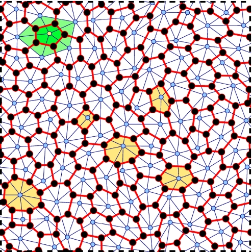
If the goal were to have a band gap only for TM polarization (electric field oscillating along the azimuthal direction), the rest of the protocol would simply be to replace each point in the original point pattern with a circular cylinder and vary the radius of the cylinders until the structure exhibits a maximum TM band gap (12–15). However, this design is poor for obtaining a band gap for TE polarization (electric field oriented in the plane). We find that the analogous optimum for TE modes is a planar, continuous trivalent network (9) (as in the case of the triangular lattice), which can be obtained from the point pattern by using the steps described in Fig. 1. Namely, construct a Delaunay tiling (16) from the original 2D point pattern and follow the steps in Fig. 1 to transform it into a tessellation of cells. Then decorate the cell edges with walls (along the azimuthal direction) of dielectric material of uniform width w and vary the width of the walls until the maximal TE band gap is obtained.
Fig. 1.
Protocol for mapping point patterns into tessellations for photonic structure design (see Design Protocol for PBGs). First, a chosen point pattern (open circles) is partitioned by using a Delaunay triangulation (thin lines). Next, the centroids of the neighboring triangles (solid circles) of a given point are connected, generating cells (thick lines) around each point, as shown for the five (green) Delaunay triangles in the upper left corner of the figure.
Finally, to obtain designs for complete PBGs, the protocol is to optimally overlap the TM and TE band gaps by decorating the vertices of the trivalent network of cell walls with circular cylinders (black circles in Fig. 1) of radius r. Then, for any given set of dielectric materials, the maximal complete PBG is achieved by varying the only two free parameters, w and r. (In practice, the optimal designs obtained by our protocol thus far have almost the same values of w and r for a given point density, so that a nearly optimal design may often be achieved without any optimization.)
Although a constrained optimization method like this is not guaranteed to produce the absolute optimum over all possible designs, in examples where the absolute optimum is known by rigorous optimization methods (8–10), our protocol produces a design whose band gap is the same within the numerical error by using exponentially less computational resources.
For the optimization of the two degrees of freedom (w and r), the photonic mode properties must be computed as parameters are varied. Because the computational requirements are modest, we employ a supercell approximation and use the conventional plane-wave expansion method (12, 17) to calculate the photonic band structure; we generate the disordered pattern within a box of side length L (with periodic boundary conditions) where L is much greater than the average interparticle spacing and take the limit as L becomes large. The PBGs for disordered heterostructures obtained by our protocol turn out to be equivalent to the fundamental band gap in periodic systems in the sense that the spectral location of the TM gap, for example, is determined by the resonant frequencies of the scattering centers (15) and always occurs between band N and N + 1, with N precisely the number of points per unit cell. This behavior underscores the relevance of the individual scattering center properties on the band gap opening and can be interpreted in terms of an effective folding of the band structure as a result of scattering on a collection of N similar (but not necessarily identical) scattering units distributed hyperuniformly in space.
Results
Disordered Photonic Materials with Large, Complete PBGs.
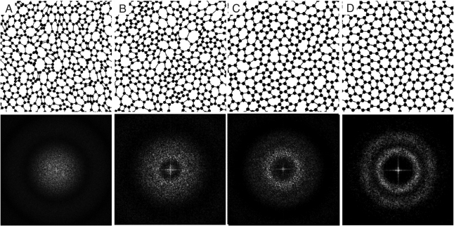
To obtain the best results, we consider a subclass of hyperuniform patterns known as “stealthy”, so named because they are transparent to incident radiation (S(k) = 0) for certain wavenumbers (7). In particular, we consider stealthy point patterns with a structure factor S(k) that is isotropic, continuous and precisely equal to zero for a finite range of wavenumbers k < kC for some positive kC. Fig. 2 presents four designs of photonic structures derived by using the protocol in Fig. 1 starting from stealthy point patterns and their structure factors, S(k).
Fig. 2.
Four designs of isotropic, dielectric heterostructures derived by using the protocol in Fig. 1 and their structure factors, S(k). (A) A disordered network design derived from a Poisson (nonhyperuniform) point pattern. (B) A network derived from a nearly hyperuniform equiluminous point pattern in which the structure factor S(k → 0) = S0>0 for k < kC. (C) A network derived from a RSA point pattern in which the structure factor S(k → 0) > 0, but there is more local geometric order than in B. D is derived from an isotropic, disordered, stealthy hyperuniform pattern, for which S(k) is precisely zero within the inner disk. Only D exhibits a complete PBG. Note the two concentric shells of sharply increased density just beyond the disk. These features sharpen as the ordering parameter χ increases; this trend coincides in real space with the exclusion zone around each particle increasing and the emergence of complete PBGs.
Stealthy hyperuniform patterns are parameterized by kC or, equivalently, χ, the fraction of wavenumbers k within the Brillouin zone that are set to zero; as χ increases, kC and the degree of hyperuniformity increase, thus, decreasing A in our definition of the number variance. When χ reaches a critical value χC(≈0.77 for 2D systems) the pattern develops long-range translational order (7).
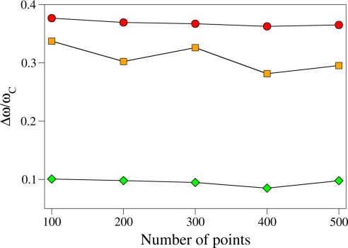
The largest PBGs in hyperuniform patterns occur in the limit of large dielectric contrast; our band structure computations assume the photonic materials are composed of silicon (with dielectric constant ε = 11.56) and air. To confirm that the computation converges and the complete PBGs are insensitive to system size, we vary the number of points per unit cell (sidelength L) ranges from n = 100−500 (see Fig. 3). For the purposes of comparison, we use a length scale a = L/, such that all patterns have the same point density 1/a2.
Fig. 3.
Optimal fractional photonic band gaps in photonic structures based on stealthy disordered hyperuniform structures of different number of points N with χ = 0.5. The plot shows that TM (red circles), TE (orange squares) and complete (green diamonds) band gaps do not vary significantly with system size.
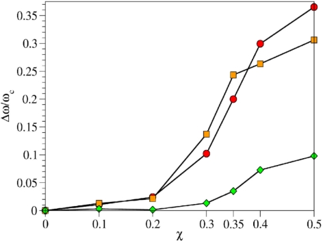
As shown in Fig. 4, significant band gap begins to open for the stealthy hyperuniform designs for sufficiently large χ ≈ 0.35 (but well below χC), at a value where there emerges a finite exclusion zone between neighboring points in the real space hyperuniform pattern (see Fig. 2). In reciprocal space, this value of χ corresponds to the emergence of a range of “forbidden” scattering, S(k) = 0 for |k|<kC for some positive kC, surrounded by a circular shell just beyond |k| = kC with increased scattering. The structures built around stealthy hyperuniform patterns with χ = 0.5 are found to exhibit remarkably large TM (of 36.5%) and TE (of 29.6%) PBGs, making them competitive with many of their periodic and quasiperiodic counterparts. More importantly, there are complete PBGs of appreciable magnitude reaching values of ≈10% of the central frequency for χ = 0.5.
Fig. 4.
A plot showing how the PBG increases as χ, or, equivalently, the degree of hyperuniformity and short-range geometric order increases. TM (red circles), TE (orange squares), and complete (green diamonds) photonic band gaps versus order parameter χ for disordered, stealthy hyperuniform derived by using the protocol in Fig. 1. The optimal structures have dimensionless cylinder radius r/a = 0.189 for the TM case, dimensionless tessellation wall thickness w/a = 0.101 for the TE case, and (r/a = 0.189, w/a = 0.031) for the TM+TE case.
Note that the density fluctuations for stealthy patterns are dramatically suppressed for wavelengths greater than 2π/kC. The lower limit 2π/kC is directly related to the midgap frequency ωC (see Fig. 2) for large enough χ, and the band width is inversely proportional to the magnitude of the density fluctuations on length scales greater than 2π/kC.
A striking feature of the PBGs is their isotropy. In ref. 10, an isotropy metric was introduced that measures the variation in band gap width as a function of incident angle. The most isotropic crystal band gap has a variation of 20%, compared with <0.1% for the hyperuniform disordered pattern in Fig. 2D. As noted in our closing discussion, isotropy can be useful for several applications.
Conditions for PBGs.
Photonic (and electronic) band gaps are commonly associated with long-range translational order and Bragg scattering, so the examples of disordered PBGs presented in this paper are counterintuitive. We argue below, based on numerical evidence and physical arguments, that complete photonic band gaps can occur in disordered systems that exhibit a combination of hyperuniformity, uniform local topology, and short-range geometric order. This argument has ramifications for electronic and phononic band gaps in disordered materials as well.
First, consider the evidence provided by numerical experiments to date. Photonic crystals are hyperuniform (an automatic consequence of periodicity) and the known examples with the largest TM, TE, and complete PBGs satisfy the two conditions (9, 18, 19). Our own numerical experiments indicate that hyperuniformity is a crucial condition. For example, we have compared results for the hyperuniform pattern in Fig. 2B with networks generated from nonhyperuniform Poisson point patterns, as in Fig. 2A; equiluminous point patterns with S(k → 0) > 0 for k < kC where the nonzero constant S (0) is made very small, as shown in Fig. 2C; and with a random-sequential absorption (RSA) point pattern (20) generated by randomly, irreversibly, and sequentially placing equal-sized circular disks in a large square box with periodic boundary conditions subject to a nonoverlap constraint until no more can be added. It has been shown that such 2D RSA packings have S(k → 0) slightly positive at k = 0 and increasing as a positive power of k for small k (21). The latter two patterns are very nearly hyperuniform, presenting similar deviations from hyperuniformity (Se−lum(k → 0) = 0.05 and SRSA(k → 0) = 0.053; and the RSA network in Fig. 2C exhibits uniform topological order (trivalency) and well-defined short-range geometric order; furthermore, these two patterns produce TM and TE band gaps separately. Yet none of the three families of patterns has been found to yield a complete PBG.
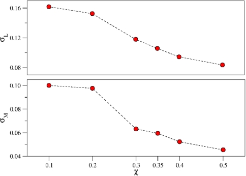
We also note that hyperuniform stealthy patterns with χ< 0.35 (and keeping all other parameters fixed) do not produce sizable, complete PBGs whereas those with χ>0.35 do, as demonstrated in Fig. 4. Fig. 5 indicates that a difference is the degree of short-range geometric order, the variance in the near-neighbor distribution of link lengths and the distance between centers of neighboring links.
Fig. 5.
A plot showing how the short-range geometric order for stealth disordered structures increases as χ, or, equivalently, the degree of hyperuniformity, increases. (Upper) The standard deviation of the average link length vs. χ for isotropic, disordered, stealthy, hyperuniform structures of the type shown in Fig. 2D. (Lower) The standard deviation of the average link separation distribution (calculated as the distance between the midpoints of two neighboring links) as a function of χ. Both plots show a significant decrease in variance as χ increases above 0.35.
Based on these and other numerical experiments, we conclude that both hyperuniformity and short-range geometric order are required to obtain substantial PBGs. In principle, the two can be varied independently, but it is notable that patterns with the highest degree of hyperuniformity also possess the highest degree of short-range geometrical order and that, for the case of stealthy patterns, both hyperuniformity and short-range geometric order increase as χ increases.
To explain how hyperuniformity and short-range geometric order, when combined with uniform local topology, can lead to a complete PBG, we first return to the point that the band gaps we have found arise in the limit of large dielectric constant ratio. In this limit and for the optimal link widths and cylinder radii, the interaction with electromagnetic waves is in the Mie scattering limit. At frequencies near the Mie resonances (which coincide with the PBG lower band edge frequencies), the scattering of TM electromagnetic waves in a heterostructure composed of parallel cylinders is similar to the scattering of electrons by atomic orbitals in cases where the tight-binding approximation can be reliably applied (22). The same applies for TE modes for any one direction k if, instead of parallel azimuthal cylinders, there are parallel thick lines (or walls in the azimuthal direction) in the plane and oriented perpendicular to k; however, to obtain a complete band gap, some compromise must be found to enable band gap for all directions k. We conjecture, based on comparison with rigorous optimization results, our own numerical experiments, and arguments below, that uniform local topology is advantageous for forming optimal band gaps. In two dimensions, this condition is easiest to achieve in disordered structures without disrupting the short-range geometric order if the networks are trivalent.
If the arrangement of dielectrics has local geometric order (the variance in link lengths and interlink distances is small), the propagation of light in the limit of high dielectric constant ratio is described by a tight binding model with nearly uniform coefficients. In the analogous electronic problem, Weaire and Thorpe (23, 24) proved that band gaps can exist in continuous random tetrahedrally coordinated networks, commonly used as models for amorphous silicon and germanium. In addition to tight binding with nearly uniform coefficients, the derivation required uniform tetrahedral coordination. (Weaire and Thorpe call networks satisfying these conditions “topologically disordered”.) The analogy in two dimensions is a trivalent network. Although their proof discussed three dimensions and tetrahedral coordination specifically, we find that it can generalize to other dimensions and networks with different uniform coordination. Note that our protocol automatically imposes uniform topology (e.g., trivalency in two dimensions) and limits variation of the tight binding parameters by imposing local geometric order.
To complete their proof, Weaire and Thorpe added a mild stipulation that the density has bounded variation, defined as the condition that the density remains between two finite values as the volume is taken to infinity. This condition is satisfied by any homogeneous system, hyperuniform or not, and thus is much weaker than hyperuniformity, for which σ2(R) = AR in the stealth 2D examples.
Although bounded variation may be sufficient to obtain a nonzero electronic band gap, we conjecture that hyperuniform, tetrahedrally coordinated, continuous random networks have substantially larger electronic band gaps than those that do not. This conjecture can be straightforwardly tested: The collective coordinate method described in ref. 7 combined with our protocol is a rigorous method for producing hyperuniform (as well as a range of controlled nonhyperuniform) tetrahedrally coordinated, continuous random network models. Our conjecture can be explored by constructing explicit networks and computing the electronic band gaps.
Analogous questions arise about real amorphous materials made in the laboratory: Do different methods of producing amorphous silicon and germanium result in the same degree of hyperuniformity, and is the behavior of S(k → 0) correlated with their electronic properties? The same questions apply to phononic properties of disordered materials.
This line of reasoning also explains why hyperuniformity is more important for obtaining complete photonic band gaps than electronic band gaps. For the electronic case, the only issue is whether there is a gap at all; the width and gap center frequency are not considered. For the photonic case, a gap is needed simultaneously for both TM and TE, and the gap centers must have values that allow an overlap. Also, the goal is not simply to have a gap but to have the widest gap possible. The evidence shows that hyperuniformity is highly advantageous (perhaps even essential) for meeting these added conditions.
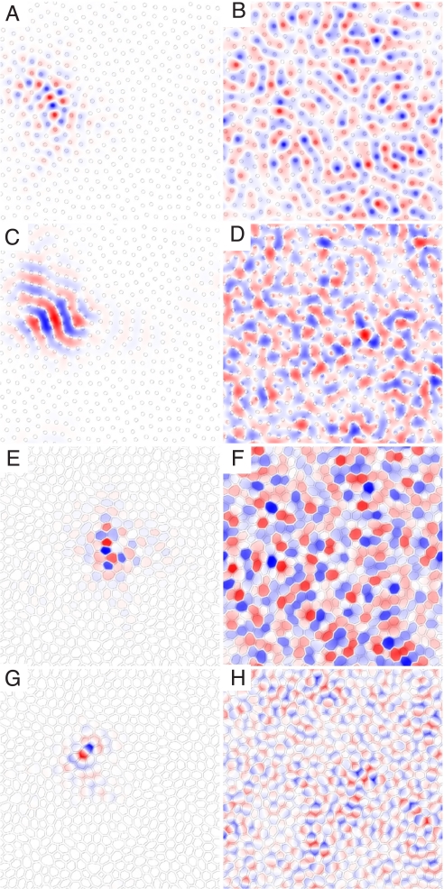
The comparison to electronic band gaps is also useful in comparing states near the band edges and continuum. For a perfectly ordered crystal (or photonic crystal), the electronic (photonic) states at the band edge are propagating such that the electrons (electromagnetic fields) sample many sites. If modest disorder is introduced, localized states begin to fill in the gap so that the states just below and just above are localized. Although formally the disordered heterostructures do not have equivalent propagating states, an analogous phenomenon occurs. In the upper four frames of Fig. 6, we compare the azimuthal electric field distribution for modes well below or well above the band gap (upper two frames), which we might call extended because the field is distributed among many sites; and then modes at the band edges, which are localized.
Fig. 6.
Electromagnetic field distribution in hyperuniform, disordered structures. (A–D) Electric field distribution in hyperuniform, disordered structures for TM polarized radiation. The structure consists of dielectric cylinders (radius r/a = 0.189 and dielectric constant ε = 11.56) in air arranged according to a hyperuniform distribution with χ = 0.5 and displays a TM PBG of 36.5% of the central frequency. Localized (A) and extended (B) modes around the lower PBG edge, and localized (C) and extended modes (D) around the upper PBG edge. (E–H) Magnetic field distribution in hyperuniform disordered structures for TE polarized radiation. The structure consists of trihedral network architecture (wall thickness w/a = 0.101 and dielectric constant ε = 11.56) obtained from a hyperuniform distribution with χ = 0.5 and displays a TE photonic band gap of 31.5% of the central frequency. Localized (E) and extended (F) modes around the lower PBG edge, and localized (G) and extended (H) modes around the upper PBG edge.
We find that the formation of the TM band gap is closely related to the formation of electromagnetic resonances localized within the dielectric cylinders (Fig. 6 A and B) and that there is a strong correlation between the scattering properties of the individual scatterers (dielectric cylinders) and the band gap location. In particular, the largest TM gap occurs when the frequency of the first Mie resonance coincides with the lower edge of the PBG (15). Analogous to the case of periodic systems, we also find that electric field for the lower band-edge states is well localized in the cylinders (the high dielectric component), thereby lowering their frequencies; and the electric field for the upper band-edge states are localized in the air fraction, increasing their frequencies (see Fig. 6 C and D). As shown in Fig. 6 E–H, an analogous behavior occurs for the azimuthal magnetic field distribution for TE modes: For the lower-edge state, the azimuthal magnetic field is mostly localized inside the air fraction and presents nodal planes that pass through the high index of refraction fraction of the structure, whereas the upper edge state displays the opposite behavior.
The discussion above accounts in a nonrigorous way for the conditions for obtaining PBGs and all of the properties observed in numerical experiments by us and others to date. We hope to develop the argument into a more precise theory in future work.
Discussion
This work demonstrates explicitly and proposes an explanation of how it is possible to design isotropic, disordered, photonic materials of arbitrary size with complete PBGs. Although photonic crystals have larger complete band gaps, disordered hyperuniform heterostructures with substantial, complete PBGs offer advantages for many applications. Disordered heterostructures are isotropic, which is advantageous for use as highly efficient isotropic thermal radiation sources (25) and waveguides with arbitrary bending angle (14). The properties of defects and channels useful for controlling the flow of light are different for disordered structures. Crystals have a unique, reproducible band structure; by contrast, the band gaps for the disordered structures have some modest random variation for different point distributions. Also, light with frequencies above or below the band edges are propagating modes that are transmitted through photonic crystals but are localized modes in the case of 2D hyperuniform disordered patterns, which give the former advantages in some applications, such as light sources or radiation harvesting materials. On the other hand, because of their compatibility with general boundary constraints, PBG structures based on disordered hyperuniform patterns can provide a flexible optical insulator platform for planar optical circuits. Moreover, eventual flaws that could seriously degrade the optical characteristics of photonic crystals and perhaps quasicrystals are likely to have less effect on disordered hyperuniform structures, therefore relaxing fabrication constraints. The results presented here are obtained for 2D structures, but a direct extension of our tessellation algorithm to 3D can be used to produces hyperuniform tetravalent connected network structures. Such a tetravalent connected network decorated with dielectric cylinders along the its edges could constitute the blueprint for 3D, disordered, hyperuniform, PBG structures. [We note that the largest known 3D PBG is provided by a similar periodic tetravalent network generated from a diamond lattice (26, 27)]. Our preliminary investigation of 3D quasicrystalline patterns show that the protocol introduced here is able to generate complete PBGs in 3D quasicrystalline photonic structures, and our plan calls for investigation of 3D hyperuniform disordered structures as well. Further analysis of the character of the electromagnetic modes supported by the disordered structures and the extension to 3D systems may be able to provide a better understanding of the interplay between disorder and hyperuniformity and between localized and extended electromagnetic modes in the formation of the PBGs.
Finally, we note that the lessons learned here have broad physical implications. One is led to appreciate that all isotropic, disordered solids are not the same: As methods of synthesizing solids and heterostructures advance, it will become possible to produce different types and degrees of hyperuniformity, and, consequently, many distinct classes of materials with novel electronic, phononic and photonic properties.
Acknowledgments.
The authors thank R. Batten (Princeton University) for generating the hyperuniform and equiluminous disordered point patterns. This work was supported by National Science Foundation Grant DMR-0606415.
Footnotes
The authors declare no conflict of interest.
This article is a PNAS Direct Submission.
References
- 1.John S. Strong localization of photons in certain disordered dielectric superlattices. Phys Rev Lett. 1987;58:2486–2489. doi: 10.1103/PhysRevLett.58.2486. [DOI] [PubMed] [Google Scholar]
- 2.Yablonovitch Y. Inhibited spontaneous emission in solid-state physics and electronics. Phys Rev Lett. 1987;58:2059–2062. doi: 10.1103/PhysRevLett.58.2059. [DOI] [PubMed] [Google Scholar]
- 3.Altug H, Englund D, Vuckovic H. Ultra-fast photonic crystal nanolasers. Nat Physics. 2006;2:484–488. [Google Scholar]
- 4.EI–Kady I, Taha MMR, Su MF. Application of photonic crystals in submicron damage detection and quantification. Appl Phys Lett. 2006;88:253109. [Google Scholar]
- 5.Chutinan A, John S, Toader O. Diffractionless flow of light in all-optical micro-chips. Phys Rev Lett. 2003;90:123901–123904. doi: 10.1103/PhysRevLett.90.123901. [DOI] [PubMed] [Google Scholar]
- 6.Torquato S, Stillinger FH. Local density fluctuations, hyperuniformity, and order metrics. Phys. Rev. E. 2003;68 doi: 10.1103/PhysRevE.68.041113. 041113/1–25. [DOI] [PubMed] [Google Scholar]
- 7.Batten RD, Stillinger FH, Torquato S. Classical disordered ground states: Super-ideal gases, and stealth and equi-luminous materials. J Appl Phys. 2008;104 033504/1–12. [Google Scholar]
- 8.Kao C, Osher S, Yablonovitch E. Maximizing band gaps in 2D photonic crystals by using level set methods. Appl Phys B. 2005;81:235–244. [Google Scholar]
- 9.Sigmund O, Hougaard K. Geometric properties of optimal photonic crystals. Phys Rev Lett. 2008;100 doi: 10.1103/PhysRevLett.100.153904. 153904/1–4. [DOI] [PubMed] [Google Scholar]
- 10.Rechtsman MC, Jeong H-C, Chaikin PM, Torquato S, Steinhardt PJ. Optimized structures for photonic quasicrystals. Phys Rev Lett. 2008;101 doi: 10.1103/PhysRevLett.101.073902. 073902/1–4. [DOI] [PubMed] [Google Scholar]
- 11.Preble S, Lipson H, Lipson M. 2D photonic crystals designed by evolutionary algorithms. Appl Phys Lett. 2005;86 061111/1–3. [Google Scholar]
- 12.Joannopoulos J, Meade RD, Winn J. Photonic Crystals. Princeton: Princeton Univ Press; 1995. [Google Scholar]
- 13.Jin C, Meng X, Cheng B, Li Z, Zhang D. Photonic gap in amorphous photonic materials. Phys Rev B. 2001;63 195107/1–7. [Google Scholar]
- 14.Miyazaki H, Hase M, Miyazaki HT, Kurokawa Y, Shinya Y. Photonic material for designing arbitrarily shaped waveguides in two dimensions. Phys Rev B. 2003;67 235109/1–5. [Google Scholar]
- 15.Rockstuhl C, Peschel U, Lederer F. Correlation between single-cylinder properties and bandgap formation in photonic structures. Opt Lett. 2006;31:1741–1743. doi: 10.1364/ol.31.001741. [DOI] [PubMed] [Google Scholar]
- 16.Preparata FR, Shamos MI. Computational Geometry: An Introduction. New York: Springer; 1985. [Google Scholar]
- 17.Johnson SG, Joannopoulos JD. Block-iterative frequency-domain methods for Maxwell's equations in a planewave basis. Opt Express. 2001;8:173–190. doi: 10.1364/oe.8.000173. [DOI] [PubMed] [Google Scholar]
- 18.Fu H, Chen Y, Chen R, Chang C. Connected hexagonal photonic crystals with largest full band gap. Opt Express. 2005;13:7854–7860. doi: 10.1364/opex.13.007854. [DOI] [PubMed] [Google Scholar]
- 19.Chan CT, Datta S, Ho H-M, Soukoulis C. A7 structure: A family of photonic crystals. Phys Rev B. 1994;50:1988–1992. doi: 10.1103/physrevb.50.1988. [DOI] [PubMed] [Google Scholar]
- 20.Torquato S. Random Heterogeneous Materials: Microstructure and Macroscopic Properties. New York: Springer; 2002. [Google Scholar]
- 21.Torquato S, Uche OU, Stillinger FH. Random sequential addition of hard spheres in high Euclidean dimensions. Phys Rev E. 2006;74 doi: 10.1103/PhysRevE.74.061308. 061308/1–16. [DOI] [PubMed] [Google Scholar]
- 22.Lidoriks E, Sigalas MM, Economou EN, Soukoulis CM. Tight-binding parametrization for photonic band gap materials. Phys Rev Lett. 1998;81:1405–1409. [Google Scholar]
- 23.Weaire D. Existence of a gap in the electronic density of states of a tetrahedrally bonded solid of arbitrary structure. Phys Rev Lett. 1971;26:1541–1543. [Google Scholar]
- 24.Weaire D, Thorpe MF. Electronic properties of an amorphous solid I A simple tight-binding theory. Phys Rev B. 1971;4:2508–2520. [Google Scholar]
- 25.Florescu M, Busch K, Dowling JP. Thermal radiation in photonic crystals. Phys Rev B. 2007;75 201101(R)/1–4. [Google Scholar]
- 26.Ho KM, Chan CT, Soukoulis CM. Existence of a photonic band gap in periodic dielectric structures. Phys Rev Lett. 1990;65:3152–3155. doi: 10.1103/PhysRevLett.65.3152. [DOI] [PubMed] [Google Scholar]
- 27.Maldovan M, Thomas LE. Diamond-structured photonic crystals. Nat Mater. 2004;3:593–600. doi: 10.1038/nmat1201. [DOI] [PubMed] [Google Scholar]
- 28.Florescu M, Torquato S, Steinhardt P. Complete band gaps in 2D photonic quasicrystals. Phys Rev B. 2009;80 155112/1–7. [Google Scholar]


