Abstract
Single- and multiple-nanopore membranes are both highly interesting for biosensing and separation processes, as well as their ability to mimic biological membranes. The density of pores, their shape, and their surface chemistry are the key factors that determine membrane transport and separation capabilities. Here, we report silicon nitride (SiN) membranes with fully controlled porosity, pore geometry, and pore surface chemistry. An ultrathin freestanding SiN platform is described with conical or double-conical nanopores of diameters as small as several nanometers, prepared by the track-etching technique. This technique allows the membrane porosity to be tuned from one to billions of pores per square centimeter. We demonstrate the separation capabilities of these membranes by discrimination of dye and protein molecules based on their charge and size. This separation process is based on an electrostatic mechanism and operates in physiological electrolyte conditions. As we have also shown, the separation capabilities can be tuned by chemically modifying the pore walls. Compared with typical membranes with cylindrical pores, the conical and double-conical pores reported here allow for higher fluxes, a critical advantage in separation applications. In addition, the conical pore shape results in a shorter effective length, which gives advantages for single biomolecule detection applications such as nanopore-based DNA analysis.
Keywords: ion track-etching, nanofluidics, filtration, SiN
Membrane technologies lie at the heart of many industrial and academic applications (1–5). High porosity membranes with application-dependent pore sizes are used in desalination, separation of molecules or particles, and other industrial processes. In the search for new membrane systems, emphasis is put on narrowing the pore size distribution, improving the chemical and mechanical robustness of the membranes, and obtaining high fluxes with low energy input (6). Membranes with single nanopores are also of great interest as a biosensing platform for detecting and characterization of single biomolecules such as DNA (7–9).
There have been many reports on preparation of membranes with well-defined pore geometry in polymer and inorganic materials (7–16). There have also been studies on thin membrane platforms containing free standing polymer membranes (17–19), inverse opals (20) as well as protein (21), and block copolymer membranes (22–24). To provide improved membrane robustness, allow miniaturization, as well as the possibility to integrate with other ionic and electronic devices, silicon-based platforms are the perfect choice.
Current techniques for producing silicon membranes with well-defined pores allow preparation of samples with extreme porosities, either highly porous or a single pore, but nothing in between. Highly porous ultrathin silicon membranes can be obtained by thermally annealing thin silicon films, which results in spontaneous pore formation (25, 26). The pore diameter can be controlled with high precision by choosing appropriate annealing conditions. This method does not allow control over the number of pores. Pores can also be fabricated one by one using ion beam sculpting (27), focused ion beam drilling (28), e-beam lithography (29), or e-beam drilling in a transmission electron microscope (TEM) (30). Although these serial approaches can be applied to various silicon and even polymer materials, they are suitable only for preparation of membranes with low numbers of pores. None of the above techniques give the possibility of tuning the geometry of the pores.
Here, we report a very versatile fabrication method for ultrathin, free standing silicon nitride (SiN) membranes containing conical and double-conical pores prepared by the ion track-etching (ITE) technique (31), together with a study of their transport properties. The ITE technique is based on irradiating a film with accelerated heavy ions, and subsequent chemical etching of the irradiated sample. The number of heavy ions corresponds to the number of fabricated pores. The technique has been used for membrane production for more than four decades (32); however, most of track-etched membranes are made in polymer films with thicknesses of at least several micrometers (16). In contrast, the ITE SiN membranes reported here have thicknesses of ∼100 nm, and the pore diameter can be made as small as 1 nm. The membranes can also withstand very harsh chemical conditions not tolerated by polymer membranes, such as piranha treatment (a heated mixture of H2SO4 and H2O2) and high temperatures. The ultrathin nanoporous SiN membranes presented here provide excellent separation capability based on electric charge and size of the permeate species. We show that the well-known SiN surface chemistry provides a convenient starting point for chemical functionalization of the pore walls to tailor these separation capabilities. In addition, such membranes constitute an attractive platform for biosensing (33). First, controlling the number of swift heavy ions that are used in the irradiation directly controls the number of pores. Single-ion irradiation available at the GSI Helmholtzzentrum für Schwerionenforschung, Darmstadt, Germany, allows the preparation of single pore membranes (34). Second, the conical and double conical shapes of the pores with tunable opening angles, together with the ultrathin character of these membranes (free standing SiN membranes with 20-nm thickness are routinely fabricated by common microfabrication techniques), offer a versatile platform for biomolecule translocation and separation experiments, such as single-molecule DNA analysis (7–9).
Results and Discussion
Nanopore Shapes and Fabrication.
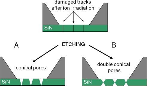
The fabrication procedure starts with preparation of SiN freestanding films, as has been well documented previously (e.g., for TEM windows) (35). The SiN films used in this study had an initial thickness of 300 nm. The films were then irradiated with energetic heavy ions (Bi or Xe) of total kinetic energy in the GeV range, which led to formation of damaged tracks (Fig. 1). Formation of damaged tracks in SiN upon Bi irradiation has been previously confirmed by TEM studies (36). We found that the damaged tracks in SiN films could be chemically developed to nanopores of specific shapes, depending on the etchant and etching arrangement used. As an example we present the fabrication of conical and double-conical nanopores using concentrated H3PO4 and HF as the etchants (Fig. 1).
Fig. 1.
Fabrication of SiN membranes with tunable porosity and pore geometry. Suspended films of SiN are subjected to heavy ion irradiation. After the irradiation with energetic ions, the damaged tracks can be etched chemically. (A) Conical pores are formed when the access of the etching agent is hindered from one side of the membrane. (B) Double conical (hour-glass) shape of pores is formed when the etching is performed from both sides of the membrane.
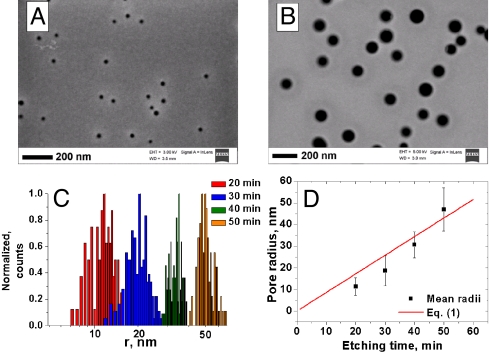
Etching time is the main parameter that controls the pore radius and also influences the membrane thickness. Examples in Fig. 2 A and B show SEM images of conically shaped nanopores prepared by etching a 300-nm-thick SiN film, which had been previously irradiated with 109 Bi ions per cm2. The irradiated film was placed at the bottom of a beaker filled with 150 °C concentrated H3PO4 so that the etchant had a free access only to one side of the SiN film (Fig. 1A). This asymmetric etching led to the formation of conical pores. Only the large openings, referred to as the bases, of the pores are shown, because few-nanometer diameter small openings, or tips, cannot be unambiguously resolved by SEM. Fig. 2C shows the base radii distributions obtained by analyzing SEM images of membranes etched in H3PO4 for various times between 20 and 50 min. It should be noted that the limiting diameter of such membranes, and thus their molecular mass cut off, is determined by the tip opening of the conical pores, not by the base radius. Narrow distributions of base radii shown in Fig. 2C suggest that the distributions of tip openings should be correspondingly tight.
Fig. 2.
Tuning pore diameter in ITE SiN membranes by etching time. SEM images and radius distributions of membranes with conical pores, which were obtained by etching irradiated SiN films in H3PO4 for 20 min (A) and 50 min (B). The images show the large opening of the conical pores; the small opening could not be resolved with SEM for low etching times. (C) Pore radius distributions at different etching times. (D) Mean of the pore size distribution shown in C as a function of etching time; the red line presents plot of Eq. 1 for g = 1.3 nm/min.
Conical nanopores are formed due to the competition of two etching rates: g, the nonspecific etching rate of the bulk material, and v, the etching rate along the damaged track. The base radius, A, can be then expressed in terms of those two unknowns and the etching time t as (31):
Fig. 2D shows a plot of Eq. 1 compared with the experimental base radii determined from the mean of the distributions in Fig. 2C. As seen from Fig. 2D, the pore diameter increases with the etching time in a linear fashion, in good agreement with Eq. 1.
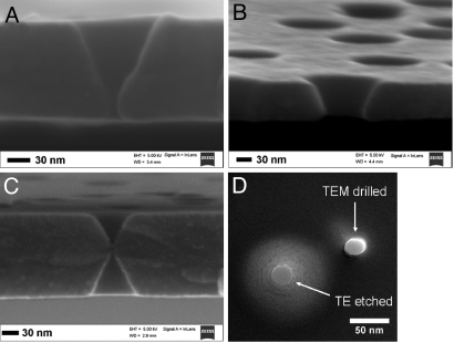
To confirm the conical shape of SiN nanopores, cross-sections of the membranes were studied by SEM. Fig. 3 A and B shows cross-sections of membranes prepared by chemical etching of Bi-irradiated SiN films. The opening angle (α) of the conical pores was determined to be ∼23°, and this value was independent of the etching time. The angle was independently confirmed by TEM. The relation α = arcsin(g/v) estimates the ratio of the two etching rates, g/v ∼0.39. The bulk material etching rate (g) was also estimated from SEM images by measuring changes of the film thickness with etching time. Values of g for our etching conditions were g = 1.5 ± 0.2 nm/min, which is in good agreement with the values reported earlier (37). From the opening angle, the etching rate along the track v was then estimated to be v ∼4.0 nm/min, approximately three times faster than the bulk etching rate. The ITE technique applied for SiN films is thus best suited for preparation of thin membranes with thicknesses up to several hundreds nanometers. It is also possible to prepare pores in thicker films; however, the much longer etching times required to open the pores will lead to very large and potentially overlapping base openings.
Fig. 3.
Examples of different pore shapes in tracked-etched SiN membranes. The etching time controls the pore radius and partially the membrane thickness. (A and B) Cross-sections of membranes containing conically shaped nanopores. The pores were obtained by etching Bi-irradiated SiN films in H3PO4 for 40 min (A), and 50 min (B). (C) Cross-section of a membrane containing double-conical nanopores. The pores were obtained by etching Bi-irradiated SiN film in H3PO4 for 30 min. The film was suspended in the etchant so that the etching could occur freely from both sides. (D) TEM images of a nanopore fabricated by the ion track etching (ITE) technique together with a pore that was fabricated by e-beam drilling using TEM. The conical shape of the ITE nanopore is responsible for the distinct halo around the pore.
Overlapping pores can also be created already at the heavy ion irradiation step in which two or even more energetic ions might hit the membrane very close to each other (38). For the irradiation density of 109 ions per cm2 and pores with a diameter of 35 nm (it is a significantly larger diameter than the one used for the separation experiments, see below), the probability for a pore to overlap with another pore is low, ≈3.8%, whereas the probability of triple overlapping pores is only ≈0.14% (38). We therefore expect that these double and triple pores will not significantly change separation capabilities of the membranes. Overlapping of pores on the side with the big pore openings will not influence separation properties either, because the separation is determined only by the tip region of the pores.
Fig. 3A shows that the pore tip openings in our SiN membranes are slightly flared, which is likely due to our etching set-up. The films were lying flat in a beaker, pore tip side down, without any sealant to prevent etchant getting underneath. As a result, etchant access was only partially blocked, leading to a small but nonzero etching rate on the tip side. It should also be noted that the etching progress can easily be monitored by the naked eye as changes in the thickness-dependent interference color of the membrane support. Direct monitoring of nanopore formation will be achieved in future using a feedback circuit based on the transpore current, as is routinely done with polymer membranes (39).
Fabrication of double-conical nanopores in SiN films irradiated with Bi ions was also demonstrated (Fig. 3C) by suspending them in a solution of H3PO4 so that the etching solution had free access to both sides of the membrane (Fig. 1B). The opening angle α of the double conical nanopores is similar to that observed for conical pores (∼23°).
It is well known that lighter ions produce much less damage in an irradiated material compared with heavier ions (31). To test the effect of lighter ions on pore formation, 300-nm-thick SiN films were irradiated with energetic Xe ions. We found that the etching rate along the track is significantly lower for Xe-irradiated compared with Bi-irradiated films. For example, Bi-irradiated films etched for 50 min had pores ∼50-nm radius (Fig. 2D), whereas Xe-irradiated films etched for the same duration had pores <15-nm radius. Consequently, pores obtained by Xe irradiation had a lower final length, and a larger opening angle of α ∼50° (see Figs. S1–S6). Thus, the ratio g/v for Xe-irradiated membranes is 0.77, compared with 0.39 for Bi ions.
Fig. 3D compares TEM images of a pore prepared by ITE and a pore obtained by drilling with the TEM e-beam (30). The conical shape of the nanopore fabricated by the ITE approach is responsible for the distinct halo around the opening, whereas such halo is absent for the TEM drilled pore. This conical pore shape can be advantageous in single molecule experiments such as nanopore-based DNA analysis. Its shorter effective length allows a higher signal-to-noise ratio due to increased ion currents and higher resolution (7–9).
Application of ITE SiN Membranes in Separation Processes.
Separation of charged molecules.
As a result of the fabrication process (irradiation and etching), the membrane surface and pore walls are covered with silanol groups similar to those at silica surfaces. For SiN, the point of zero charge depends greatly on the method of preparation and the stoichiometry of the material (40). We have found that the surface of our ITE SiN membranes is heavily negatively charged (i.e., the Si–OH groups are deprotonated) at least for pH > 5. SiN membranes prepared by the ITE technique are therefore useful for separation of molecules by charge, which we tested by performing separation experiments with two oppositely charged fluorescent dyes: rhodamine 123 (MW ∼ 400, charge: +1), and Alexa Fluor 568 (MW ∼ 800, charge: −3). Due to the negatively charged silanol groups, the negatively charged dye (Alexa Fluor) should be excluded from the pores by electrostatic forces (16, 41, 42). As a consequence, only the positive dye (rhodamine) was expected to pass through the membrane. To study the passage of the fluorophores through ITE SiN membranes, we adopted a simple and effective approach proposed by Striemer et al. (25) Briefly, the fluorophores' permeation was imaged by a confocal fluorescent microscope focused on the membrane edge, to record the diffusion of permeant fluorophores away from the membrane, perpendicular to its surface. The fluorescence signal was normalized by the intensity directly over the membrane, i.e., the feed solution. This normalized signal gives unambiguous information about the relative fluxes of different species through the membrane. Details of the experimental set-up can be found in Figs. S1–S6. SiN membranes used in the permeation experiments were obtained by etching irradiated films in H3PO4 for 40 min. According to our SEM studies of the membrane cross-sections, as well as fluorescence transport experiments, 40 min corresponds to the mean time that is needed to etch through heavy ion tracks in 300-nm-thick SiN films. Based on transport properties of the membranes, it is safe to estimate that the tip opening of the pores was <10 nm.
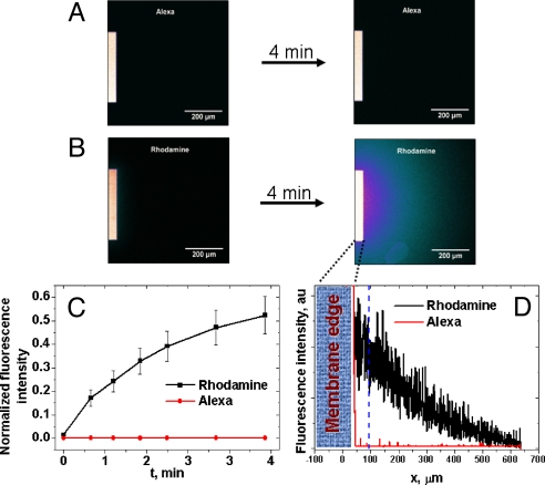
Fig. 4 summarizes the permeation experiments performed with Alexa and rhodamine. It is clear that the initial and the final frames for the Alexa dye permeation (Fig. 4A) are almost identical, i.e., there is no fluorescence signal spreading over the membrane support in the course of 4 min. This observation confirms that the membrane indeed does not allow the negative dye to pass through. In contrast, positively charged rhodamine freely diffuses through the membrane forming a bright fluorescence image (Fig. 4B). Animations showing the 4-min time course of the diffusion experiments are included in Movies S1–S5. Fig. 4C summarizes the permeation kinetics for each dye. The fluorescence intensity was measured at a position 50 μm away from the membrane edge and subsequently normalized to the intensity at the middle of the membrane in the first frame. Fig. 4D shows cross sections of the final frames for the Alexa and rhodamine permeation experiments (Fig. 4 A and B Right). The zero fluorescence signal for the Alexa case confirms that SiN membranes can separate ionic species based on their charge.
Fig. 4.
Simultaneous filtration of two low molecular mass fluorophores with positive and negative charges through ITE SiN membranes. The membranes were obtained by etching SiN films irradiated Bi ions for 40 min. (A) Fluorescent image of passage of the Alexa dye through a negatively charged SiN membrane. (Left) Initial frame taken immediately after introduction of the feeding solution on top of the membrane; (Right) image was acquired 4 min later. See animations in Movies S1–S5. It is clear that the initial and the final frames are almost identical: the membrane rejects the negative dye very efficiently. (B) Passage of rhodamine through a negatively charged SiN membrane. Since this dye is positive, it diffuses freely through the membrane thus forming a bright final frame. (C) Kinetics of the passage of the Alexa (red ♦) and rhodamine (■) dyes. The fluorescence intensity was measured from the level at the position 50 μm away from the membrane edge (see dashed line in D), and normalized to the intensity in the first frame measured in the middle of the membrane. (D) Cross-section of the final frames taken after 4 min shown on A and B; note that the fluorescence intensity of the Alexa dye (red line) is very low compared with the rhodamine trace (black line).
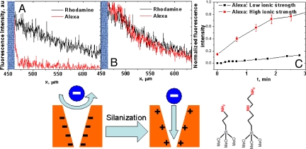
The silanol groups present on the membrane surface and pore walls can be modified with silanes to introduce desired chemical functionalities. To provide further confirmation of the electrostatic character of the Alexa/rhodamine separation, we modified the SiN membranes with silanes containing amine groups (Fig. 5). As a result, at pH < 9, a positively charged membrane was obtained, which was expected to exhibit reversed selectivity, i.e., transport a negative dye and block a positive dye. Comparing the cross-section of the two fluorescence images shown in Fig. 5 A and B indicates that the flux of the negative species (Alexa Fluor 568) was indeed significantly increased compared with the unmodified membranes. The aminated membrane, however, became almost nonselective, i.e., the fluxes of rhodamine and Alexa are the same. To understand the results one has to consider electrostatic interactions between a charged pore and two fluorescent probes that carry different charges both in magnitude and sign. Fig. 4 shows that when Alexa carrying −3e charge is a co-ion in a negatively charged pore, the pore rejects the dye very effectively, and transports only the positively charged rhodamine that carries +1e charge. If the Alexa acts as a counterion, as it is the case in a positively charged pore, the nanochannel selectivity toward either dye, i.e., rhodamine or Alexa can drastically decrease. It is because the more charged counterion screens the surface charges over a shorter distance compared with monovalent species resulting in overall weaker ability of a pore to distinguish between positive and negative species. As a further support of this hypothesis, we performed modeling of ionic concentrations and electric potential inside a charged nanopore using the Poisson–Nernst–Planck equations. The modeling was performed for an 8 nm in diameter cylindrical nanopore with either positive or negative surface charges in contact with 3:1 electrolyte (see Figs. S1–S6). The electric potential in the pore is indeed lower when the pore is in contact with polyvalent counterions. It is also important to note that the concentrations of fluorescent probes are much lower than the concentration of the supporting electrolyte, which further complicates the description of the problem. Another factor which can account for weaker separation properties of aminated membranes is an incomplete silanization process, which would result in lower positive surface charge densities compared with the starting hydroxyl group densities.
Fig. 5.
Chemical modification of track-etched SiN membranes. Transport properties as a function of surface charges and ionic strength of the supporting electrolyte. The membranes were obtained by etching Bi ions irradiated SiN films for 40 min. (A and B) Cross-sections of fluorescent images acquired 2 min after introducing the dye on top of an unmodified membrane (A), and a membrane with immobilized aminosilanes (B); data for rhodamine (black line), and data for Alexa (red line). Flux of the Alexa dye significantly increased after the membrane had been modified with amines: compare the traces (red line) in A and B. (C) Permeation kinetics of the Alexa dye through an unmodified SiN membrane. Two solutions of the Alexa dye were prepared: in 1 mM MES (■), and 1 mM MES with 100 mM KCl (red ■). At the higher ionic strength solution, the intrinsic negative charge of an unmodified membrane is screened over shorter distances, which results in high fluxes of the negative Alexa dye.
The ionic strength of the electrolyte solution in the charged pores influences the screening length of the surface charges and consequently the ionic concentration profiles inside the nanopores (42). A high salt concentration screens surface charge over much shorter lengths; therefore, increasing the ionic strength of the supporting electrolyte was expected to decrease the electrostatically-derived selectivity of the membranes toward Alexa and rhodamine. Fig. 5C shows the flux of Alexa dye through an unmodified (i.e., negatively charged) membrane in two solutions: (i) a low ionic strength solution of 1 mM MES, and (ii) a higher ionic strength solution of 1 mM MES and 100 mM KCl. As expected, the flux of the negatively charged Alexa dye is significantly increased in the higher ionic strength medium, which provides further evidence for the electrostatic mechanism for the selectivity of the membrane. It should, however, be noted that, for smaller etching times, our membranes exhibited finite selectivity toward the cationic dye even in a solution of 1 M KCl, in which the screening length is ∼0.3 nm (see Figs. S1–S6). This observation supports the nanometer size of our pores.
Separation by size.
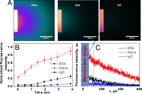
To demonstrate the size separation capabilities of our membranes, we also performed permeation experiments with proteins of different sizes (Fig. 6). We used BSA (molecular mass of 67 kDa), labeled with Alexa Fluor 488, and IgG (molecular mass of 150 kDa), labeled with Alexa Fluor 680. To reduce the electrostatic influence of the membrane surface charge, as well as charges on the proteins on the separation process, the experiments were performed in high ionic strength conditions of 0.5 M KCl buffered with MES to pH 5.5. 0.5 M KCl screens all of the charges very effectively so that the influence of isoelectric point of the proteins on the final separation outcome was minimized. Even though BSA and IgG have diffusion coefficients that differ by no more than 40%, fluxes of these proteins through our membrane were found different by more than three times, thus confirming that our membranes are also well-suited for size-based separation processes. The protein fluxes in 0.5 M KCl were also compared with the transmembrane transport of the Alexa dye. A high flux of the negatively charged Alexa through the negatively charged SiN membranes indicates that the effect of charges on the separation process was indeed negligible.
Fig. 6.
Permeation of Alexa Fluor, BSA, and IgG proteins through ITE SiN membranes. Fluorescent images were taken 4 min after introduction of the feed solution on top of the membrane. (A) Fluorescence images due to permeation of the Alexa dye (Left), BSA (Center), and IgG (Right). (B) Kinetics of the permeation process for BSA, Alexa, and IgG. (C) Fluorescence intensity at the cross-section shown in A.
Conclusions
We have presented here ultrathin freestanding SiN membranes with fully-controlled porosity, pore geometry, and pore surface chemistry. Porosity can be tuned from one to billions of pores per square centimeter. In contrast, existing techniques either drill pores one by one, or produce only extremely porous membranes. The fabrication method presented here is based on the track-etching technique where the number of pores is given by the number of irradiating ions, whereas the pore shape is controlled by the chemical etching step. The presented and previously undescribed track-etched SiN membranes feature excellent selectivity in filtration processes, based on the permeate charge and size. Negatively charged membranes distinguish between the positively-charged rhodamine dye and the negative Alexa fluorophore, so that only the positive molecule is transported. The membranes also act as molecular sieves, selecting the smaller BSA over the larger IgG protein.
The ITE technique allows for fabrication of thin membranes not only in SiN but also in other inorganic materials, for example, SiO2 (43). Tuning the etching conditions is expected to result in other pore geometries (e.g., cylindrical, cigar-shaped, etc.). The next step will be to improve the membrane fabrication process by introducing a controlled etching system (39), which is especially crucial for preparation of single-pore membranes. SiN membranes with controlled porosity will find various applications in sensing, filtration, separation, and dialysis processes, both on the laboratory and industrial scales. The application spectrum can be enhanced by chemical functionalization and immobilization of recognition agents (e.g., DNA and proteins). Contributing to the efforts to miniaturize biotechnological devices, our SiN membranes enable the development of more complex nanofluidic systems and ionic circuits.
Methods
Fabrication of Membranes.
The membrane arrays were fabricated on a 100-mm diameter × 500-μm 〈100〉 Si wafer with a 300-nm SiN film deposited by the low-pressure chemical vapor deposition process. The film was patterned using standard photolithographic techniques and subjected to heavy ion irradiation at the Flerov Laboratory of Nuclear Reactions (Dubna, Russia). Irradiations with 0.71-GeV Bi ions and 170 MeV Xe ions were performed in the U-400 and the IC-100 cyclotrons, respectively. SiN wafers were exposed to 108 and 109 ions per cm2. Energy losses of the ions in SiN were calculated using the stopping and range of ions in matter (SRIM) code (see www.srim.org) and were equal to 36 MeV/μm (for Bi) and 22 MeV/μm (for Xe). The pores were developed by etching the irradiated SiN films in concentrated H3PO4 heated to 150 °C on a hot plate. In addition, chemical etching in HF was performed, which also resulted in the formation of pores (see Figs. S1–S6).
Chemical Modification with Silanes.
SiN membranes were thoroughly washed in deionized water and immersed in the modification solution of 1% silane prepared in pure ethanol and 5% deionized water. Two silanes containing amine groups were used: (3-aminopropyl)trimethoxysilane or [3-(2-aminoethylamino)propyl]trimethoxysilane) (Fig. 5). Both these chemicals resulted in positively charged membranes. We also performed a successful silanization reaction using 2% silane in pure toluene. All these membranes showed similar results in the fluorescence permeation experiments. The silanization reactions were performed for 1 h followed by rinsing in a solvent and 1–3-h baking at 120 °C on a hot plate.
Fluorescence Measurements.
Alexa Fluor 568, rhodamine 123, BSA labeled with Alexa Fluor 488 (labeling efficiency 1:7), and IgG labeled with Alexa Fluor 680 (labeling efficiency 1:4) were purchased from Pierce. Before the permeation experiments, the succinimidyl group in Alexa Fluor 568 dye was hydrolyzed by keeping a water solution of the Alexa dye for over a week at room temperature or by reaction with γ-aminobutyric acid (Aldrich). The hydrolysis and reaction with γ-aminobutyric acid resulted in the formation of a negatively charged carboxyl group; 30 μM solutions of Alexa and rhodamine in 1 mM MES pH 5.5 buffer were used in the separation experiments. The ionic strength of the solutions was controlled by addition of corresponding amounts of KCl. The experiments with proteins were performed in 1 mM MES, 500 mM KCl, pH 5.5 buffer as a supporting electrolyte. The solution contained 50 μΜ Alexa Fluor 568, 7 μΜ BSA, and 2 μM IgG. Different labeling efficiencies and concentrations of the proteins did not influence the quantitative results of the permeation experiments (Fig. 6B), because the fluorescence intensity was normalized to the intensity of the feed solution, as imaged and measured in the middle of the membrane. The fluorescent experiments were performed using an Olympus Fluoview FV1000 confocal microscope. Mixtures of fluorophores were imaged simultaneously using several channels of the microscope. Fluorescent experiments with dye molecules and proteins were performed with membranes, which were irradiated with 108 and 109 ions per cm2, respectively. The selectivity experiments were performed with membranes etched in H3PO4, at 150 °C for 40 min.
SEM and TEM Images.
SEM images were obtained using a Zeiss Ultra Plus microscope. All images except for the images of cross-sections were recorded after a thin layer (1–2 nm) of Ir had been sputtered on the membranes. The pore shown in Fig. 3D was drilled and its TEM image captured using JEOL 2010F field-emission TEM operating at 200 kV.
Supplementary Material
Acknowledgments.
We thank V. A. Skuratov for his assistance in irradiating SiN films, Dr. Sergei N. Smirnov for stimulating discussions, and Dr. Stefan Howorka for careful reading of the manuscript and his comments. The authors acknowledge the provision of the instrumentation in the Carl Zeiss Center of Excellence at UCI by Carl Zeiss SMT. This work was supported by National Science Foundation Grant CHE 0747237. Z.S.S. is an Alfred P. Sloan Fellow.
Footnotes
The authors declare no conflict of interest.
This article contains supporting information online at www.pnas.org/cgi/content/full/0911450106/DCSupplemental.
References
- 1.Mulder M. Basic Principles of Membrane Technology. Dordrecht, The Netherlands: Kluwer; 1996. [Google Scholar]
- 2.Baker RW. Membrane Technology and Applications. Hoboken, NJ: Wiley; 2004. [Google Scholar]
- 3.Petersen RJ. Composite reverse osmosis and nanofiltration membranes. J Membr Sci. 1993;83:81–150. [Google Scholar]
- 4.Vandezande P, Gevers LEM, Vankelecom IFJ. Solvent resistant nanofiltration: Separating on a molecular level. Chem Soc Rev. 2008;37:365–405. doi: 10.1039/b610848m. [DOI] [PubMed] [Google Scholar]
- 5.Schäfer AI, Fane AG, Waite ID, editors. Nanofiltration: Principles and Applications. New York: Elsevier; 2005. [Google Scholar]
- 6.Shannon MA, et al. Science and technology for water purification in the coming decades. Nature. 2008;452:301–310. doi: 10.1038/nature06599. [DOI] [PubMed] [Google Scholar]
- 7.Dekker C. Solid state nanopores. Nat Nanotechnol. 2007;2:209–215. doi: 10.1038/nnano.2007.27. [DOI] [PubMed] [Google Scholar]
- 8.Branton D, et al. The potential and challenges of nanopore sequencing. Nat Biotechnol. 2008;26:1146–1153. doi: 10.1038/nbt.1495. [DOI] [PMC free article] [PubMed] [Google Scholar]
- 9.Healy K. Nanopore-based single-molecule DNA analysis. Nanomed. 2007;2:459–481. doi: 10.2217/17435889.2.4.459. [DOI] [PubMed] [Google Scholar]
- 10.Nishizawa M, Menon VP, Martin CR. Metal nanotubule membranes with electrochemically switchable ion-transport selectivity. Science. 1995;268:700–702. doi: 10.1126/science.268.5211.700. [DOI] [PubMed] [Google Scholar]
- 11.Kohli P, et al. DNA-functionalized nanotube membranes for single-base mismatch DNA selectivity. Science. 2004;305:984–986. doi: 10.1126/science.1100024. [DOI] [PubMed] [Google Scholar]
- 12.Masuda H, et al. Highly ordered nanochannel-array architecture in anodic alumina. Appl Phys Lett. 1997;71:2770–2772. [Google Scholar]
- 13.Holt JK, et al. Fast mass transport through sub-2-nanometer carbon nanotubes. Science. 2006;312:1034–1037. doi: 10.1126/science.1126298. [DOI] [PubMed] [Google Scholar]
- 14.Fornasiero F, et al. Ion exclusion by sub-2-nm carbon nanotube pores. Proc Natl Acad Sci USA. 2008;105:17250–17255. doi: 10.1073/pnas.0710437105. [DOI] [PMC free article] [PubMed] [Google Scholar]
- 15.Han J, Fu J, Schoch RB. Molecular sieving using nanofilters: Past, present and future. Lab Chip. 2008;8:23–33. doi: 10.1039//b714128a. [DOI] [PMC free article] [PubMed] [Google Scholar]
- 16.Savariar EN, Krishnamoorthy K, Thayumanavan S. Molecular discrimination inside polymer nanotubules. Nat Nanotechnol. 2008;3:112–117. doi: 10.1038/nnano.2008.6. [DOI] [PubMed] [Google Scholar]
- 17.Vendamme R, Onoue S-Y, Nakao A, Kunitake T. Robust free-standing nanomembranes of organic/inorganic interpenetrating networks. Nat Mater. 2006;5:494–501. doi: 10.1038/nmat1655. [DOI] [PubMed] [Google Scholar]
- 18.Watanabe H, Kunitake T. A Large, freestanding, 20 nm thick nanomembrane based on an epoxy resin. Adv Mater. 2007;19:909–912. [Google Scholar]
- 19.Fujikawa S, Muto E, Kunitake T. Nanochannel design by molecular imprinting on a free-standing ultrathin titania membrane. Lagmuir. 2009;25:11563–11568. doi: 10.1021/la9014916. [DOI] [PubMed] [Google Scholar]
- 20.Yan F, Goedel WA. A simple and effective method for the preparation of porous membranes with three-dimensionally arranged pores. Adv Mater. 2004;16:911–915. [Google Scholar]
- 21.Peng X, Jin J, Nakamura Y, Ohno T, Ichinose I. Ultrafast permeation of water through protein-based membranes. Nat Nanotechnol. 2009;4:353–357. doi: 10.1038/nnano.2009.90. [DOI] [PubMed] [Google Scholar]
- 22.Hashimoto T, Tsutsumi K, Funaki Y. Nanoprocessing based on bicontinuous microdomains of block copolymers: Nanochannels coated with metals. Langmuir. 1997;13:6869–6872. [Google Scholar]
- 23.Uehara H, et al. Size-selective diffusion in nanoporous but flexible membranes for glucose sensors. ACS Nano. 2009;3:924–932. doi: 10.1021/nn8008728. [DOI] [PubMed] [Google Scholar]
- 24.Nuxoll EE, Hillmyer MA, Wang R, Leighton C, Siegel RA. Composite block polymer-microfabricated silicon nanoporous membrane. Appl Mater Interfaces. 2009;1:888–893. doi: 10.1021/am900013v. [DOI] [PMC free article] [PubMed] [Google Scholar]
- 25.Striemer CC, Gaborski TR, McGrath JL, Fauchet PM. Charge- and size-based separation of macromolecules using ultrathin silicon membranes. Nature. 2007;445:749–753. doi: 10.1038/nature05532. [DOI] [PubMed] [Google Scholar]
- 26.Kim E, et al. A Structure-permeability relationship of ultrathin nanoporous silicon membrane: A comparison with the nuclear envelope. J Am Chem Soc. 2008;130:4230–4231. doi: 10.1021/ja711258w. [DOI] [PMC free article] [PubMed] [Google Scholar]
- 27.Li J, et al. Ion-beam sculpting at nanometre length scales. Nature. 2001;412:166–169. doi: 10.1038/35084037. [DOI] [PubMed] [Google Scholar]
- 28.Tong HD, et al. Silicon nitride nanosieve membrane. Nano Lett. 2004;4:283–287. [Google Scholar]
- 29.Deshmukh MM, Ralph DC, Thomas M, Silcox J. Nanofabrication using stencil mask. Appl Phys Lett. 1999;75:1631–1633. [Google Scholar]
- 30.Storm AJ, Chen JH, Ling XS, Zandbergen HW, Dekker C. Fabrication of solid-state nanopores with single-nanometre precision. Nat Mater. 2003;2:537–540. doi: 10.1038/nmat941. [DOI] [PubMed] [Google Scholar]
- 31.Fleischer RL, Price PB, Walker RM. Nuclear Tracks in Solids. Principles and Applications. Berkeley, CA: Univ California Press; 1975. [Google Scholar]
- 32.Apel P. Track etching technique in membrane technology. Radiat Meas. 2001;34:559–566. [Google Scholar]
- 33.Vlassiouk I, Smirnov S. Biosensing with nanopores. In: Mercoçi A, editor. Biosensing Using Nanomaterials. Hoboken, NJ: Wiley; 2009. pp. 459–490. [Google Scholar]
- 34.Spohr R, inventor. Methods and device to generate a predetermined number of ion tracks. DE 2951376 C2. German Patent. 1983 US Patent 4369370.
- 35.Grant AW, Hu Q-H, Kasemo B. Transmission electron microscopy ‘windows’ for nanofabricated structures. Nanotechnology. 2004;15:1175–1181. [Google Scholar]
- 36.Zinkle SJ, Skuratov VA, Hoelzer DT. On the conflicting roles of ionizing radiation in ceramics. Nucl Instr Meth Phys Res B. 2002;191:758–766. [Google Scholar]
- 37.van Gelder W, Hauser VE. The etching of silicone nitride in phosphoric acid with silicon dioxide as a mask. J Electrochem Soc. 1967;114:869–872. [Google Scholar]
- 38.Riedel C, Spohr R. Correcting overlapping counts in dose calculation at high event-densities. Nucl Tracks. 1981;5:265–270. [Google Scholar]
- 39.Apel P, Korchev YE, Siwy Z, Spohr R, Yoshida M. Diode-like single-ion track membrane prepared by electro-stopping. Nucl Instr Meth Phys Res B. 2001;184:337–346. [Google Scholar]
- 40.Raiteri R, Margesin B, Grattarola M. An atomic force microscope estimation of the point of zero charge of silicon insulators. Sens Actuators B. 1998;46:126–132. [Google Scholar]
- 41.Rice CL, Whitehead R. Electrokinetic flow in a narrow cylindrical capillary. J Phys Chem. 1965;69:4017–4024. [Google Scholar]
- 42.Vlassiouk I, Smirnov S, Siwy Z. Ion selectivity of single nanochannels. Nano Lett. 2008;8:1978–1985. doi: 10.1021/nl800949k. [DOI] [PubMed] [Google Scholar]
- 43.Musket RG, Yoshiyama JM, Porter JD, Contolini RJ. Vapor etching of ion tracks in fused silica. J Appl Phys. 2002;91:5760–5764. [Google Scholar]
Associated Data
This section collects any data citations, data availability statements, or supplementary materials included in this article.


