

This work demonstrates the design, fabrication, packaging, characterization, and functionality of an electrically and fluidically active three-dimensional micro-electrode array (3D MEA) for use with neuronal cell cultures. The successful function of the device implies that this basic concept— construction of a 3D array with a layered approach—can be utilized as the basis for a new family of neural electrode arrays. The 3D MEA prototype consists of a stack of individually patterned thin films that form a cell chamber conducive to maintaining and recording the electrical activity of a long-term three-dimensional network of rat cortical neurons. Silicon electrode layers contain a polymer grid for neural branching, growth, and network formation. Along the walls of these electrode layers lie exposed gold electrodes which permit recording and stimulation of the neuronal electrical activity. Silicone elastomer micro-fluidic layers provide a means for loading dissociated neurons into the structure and serve as the artificial vasculature for nutrient supply and aeration. The fluidic layers also serve as insulation for the micro-electrodes. Cells have been shown to survive in the 3D MEA for up to 28 days, with spontaneous and evoked electrical recordings performed in that time. The micro-fluidic capability was demonstrated by flowing in the drug tetrotodoxin to influence the activity of the culture.
Introduction
Planar multi-electrode arrays (MEAs) have been developed for neural applications including brain slice recording [1,2] and dissociated cultures [3,4], to the point where commercial devices are readily available for the study of two-dimensional (2D) or monolayer networks of neurons. There is growing interest in developing three-dimensional (3D) systems that add greater fidelity to these models of the brain. In fact, many cell types have been cultured in both 2D and 3D, and significant differences in behavior have been observed [5–7]. In vitro micro-cavity impedance studies have been performed on 3D multi-cellular spheroids [8]. Compared to monolayer cultures, the spheroids better approximate the in vivo cell–cell and cell–extracellular matrix contacts that impact cell growth, differentiation, and programmed cell death [9]. The guiding hypotheses of this work are that neuronal culture systems are more realistic in 3D, inferences drawn from 3D cultures are more likely to be valid in vivo, and the development of 3D MEAs would enable advances in this science.
The state-of-the-art in 3D arrays for in vivo use includes microwire arrays [10] and silicon multi-electrode probes (e.g., arrays from Michigan [11] and Utah [12]). One group has reported a design for dual-side and double-layer electrode arrays that have been successfully tested in brain tissue samples [13]. It is possible, but sub-optimal, to insert these probes into a 3D in vitro sample. These devices do not include the capability for fluid exchange that is required by in vitro samples and do not have adequate surface area for culturing cells in a liquid media.
Progress has been made in developing arrays of post-like structures equipped with electrodes on top of these posts for in vitro recordings [14–16]. These posts allow the electrodes to protrude deeper into a slice preparation, past the layer of dead cells that form at the slice interface. The electrodes thus have threedimensionality and, for slice cultures, can yield stronger signals than the traditional monolayer cultures, but the recording space is still a 2D plane. Recently, individual patch clamp recordings have been obtained from neurons cultured deep within 3D scaffolds [17]. There are also reports of arrays specifically designed for in vitro neuronal use, constructed around the “bed of nails” concept, but with integrated micro-fluidics for additional functionality [18–20]. In one report, the micro-scaffold consisted of an 8 × 8 array of hollow micro-fabricated SU-8 towers with horizontal SU-8 cross-members, forming a 3D grid conducive to branching, growth, and increased network formation of dissociated neurons. Each micro-tower had multiple fluid ports for media delivery and two exposed gold electrodes on its outer wall to allow for electrical stimulation and recording [20]. To date, there are no reports of recorded signals with these devices. Our prototype design can be seen as an alternative approach with a similar goal.
Here we describe a new approach to constructing three-dimensional micro-electrode arrays (3D MEAs) that overcomes the packaging limitations while preserving the electrical and fluidic access needed for dissociated 3D cultures. This structure is created by fabricating, aligning, and stacking individually patterned thin films, each of which constitutes either an electrode or a fluidic layer. The micro-fluidic layers permit loading of cells, perfusion, and drug application, all of which are demonstrated. The electrode layers enable recording and stimulation of neurons, and have planar contacts compatible with commercial instrumentation. Signal acquisition, correlation of activity on multiple layers, and stimulation of network activity are demonstrated. While the device described here is clearly a prototype, the layer-by- layer concept is amenable to significant improvement in material choice and geometric layout for reduced cost, improved performance, and conformation to specific biological hypotheses.
Design and fabrication
Overview
To make the 3D MEA realizable, two key design constraints were employed. First, the footprint and contact pad layout for the 3D MEA was designed to match an existing commercial amplifier holder, whose spring-loaded pins access the contact pads from above. The micro-fluidic plumbing easily fit within the layout of the commercial MEA, permitting simultaneous electrical recording and drug application. Second, a layered, modular approach reduced processing time and costs as patterned thin films are more readily fabricated than high aspect ratio structures. This device is made of two types of layers: (1) stackable, thin electrode layers that have a physical matrix to support neuronal growth, and (2) micro-fluidic layers for nutrient delivery, waste removal, and introduction of chemical stimuli to alter neuronal responses. Alternating electrode and fluidic layers are aligned and bonded together to form the device. Neurons can be loaded either into the cavity directly or introduced through the fluidics. The electrode layers contain a grid of vias to allow neurites to extend between electrode layers. The materials have all been shown to be biocompatible.
Electrode layer fabrication
Silicon and SU-8 (MicroChem Corp., Newton, Massachusetts) were selected for the fabrication of the electrode layers, as shown in Fig. 1. The design consists of an SU-8 grid suspended over a through-hole in the underlying Si. Patterning the Ti/Au electrode lines on top of the SU-8 and patterning the through-holes in the SU-8 and Si layers are straightforward and standard processes. The electrode layer fabrication process is a combination of additive and subtractive steps (Fig. 1). The starting material is a 2-inch Si wafer with a thickness of 100 μm. To improve SU-8 adhesion, the wafer is degreased and cleaned with O2 plasma (20 s, 55 W) directly before spinning on the SU-8. On the frontside of the wafer, a layer of SU-8 2010 is spun onto the wafer to a thickness of approximately 13 μm. For the soft bake, the substrate is placed on a hotplate at room temperature (RT). The hotplate is ramped from RT to 65 °C at a rate of 7.5 °C min−1. It is held at 65 °C for 5 min and then allowed to slowly cool down to RT. An exposure dose of 140 mJ cm−2 is used to pattern the SU-8 layer. For the post-exposure bake, the substrate is placed on a hotplate at RT. The hotplate is ramped from RT to 65 °C at a rate of 7.5 °C min−1. It is held at 65 °C for 30 min and then allowed to slowly cool down to RT.
Fig. 1.

Fabrication of an electrode layer. (A) SU-8 is patterned on a thin Si wafer. (B) Ti/Au lines are patterned on the SU-8. (C) PR is spun onto the backside of the wafer. A hole is opened in the PR directly underneath the SU-8 pattern. (D) Deep Si etching removes the Si directly underneath the SU-8 grid, leaving a suspended thin membrane of SU-8.
The wafers are developed in SU-8 Developer for 3 min (MicroChem Corp., Newton, Massachusetts). Wafers are then rinsed in fresh SU-8 Developer, isopropyl alcohol, and dried with nitrogen. A hardbake is performed by placing the substrate on a RT hotplate. The hotplate is ramped to 150 °C at a rate of 7.5 °C min−1. It is held at 150 °C for 2 min and then allowed to slowly cool down to RT.
A layer of Ti/Au (50 Å, 450 Å) is deposited on the wafers, and the electrode lines are patterned and etched. Photoresist (PR, AZ 4620) is spun onto the wafer backside, and a backside aligner is used to open a hole in the PR underneath the SU-8 grid on the opposite side of the wafer. A deep Si etcher is used to dry-etch the Si through-hole. This process selectively etches Si over polymers and stops cleanly on the grid layer without any visible damage to the underlying SU-8. The bottom electrode layer is unique in a couple of ways. First, the substrate is bare glass and lacks a SU-8 layer. Glass was chosen so that the final device would permit transmitted light imaging. Also, the layer does not have a through-hole etched in the center.
Fluidic layer fabrication
Each fluidic layer lies directly on top of the bare gold electrode lines and defines the electrode area by serving as an insulating layer. Hence our electrodes are at the edges of the cell chamber. (See discussion.) PDMS was chosen as the material for the fluidic layer for its insulating properties. PDMS bonds and seals robustly to silicon and SU-8, and is biocompatible, inexpensive, and easy to work with. The fluidic layers were fabricated using soft-lithography molding techniques as shown in Fig. 2. A mold was created using SU-8 processing on a 3 inch silicon wafer. For the first fluidic layer master, a two-layer SU-8 process was used similar to a published method [21]. The first layer of SU-8 was spun on, soft baked, and exposed. This layer defined the fluidic channel. Immediately after exposure, a second layer was spun on, soft baked, exposed, and postexposure baked, and then both layers were simultaneously developed. The second layer defined two through-holes to serve as the inlet and outlet of the channel. For this prototype, all subsequent fluidic layers had no fluidics and served as insulation and spacers. These molds were created with a single SU-8 layer. Each SU-8 layer in the mold fabrication was 280 μm thick.
Fig. 2.
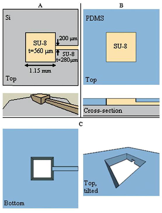
Fabrication of a fluidic layer. (A) A two-layer SU-8 structure is patterned onto a Si wafer. (B) PDMS is poured onto the mold so that it entirely covers the channel, and the taller SU-8 post creates a through-hole in the PDMS. (C) After curing, the PDMS can be peeled off of the mold to yield the structure shown here.
After the molds were fabricated, they were silanized to prevent irreversible adhesion between the Si and the PDMS. PDMS was poured onto the mold and clamped on top with a transparency film (to prevent bonding) and a glass slide. After curing, the PDMS could be peeled off of the device to yield the complete fluidic layer.
Assembly
The individual layers of the device were assembled by adapting a process developed for stacking PDMS films [22]. First, both the glass bottom electrode layer and the fluidic layer were treated with O2 plasma (100 W, 20 s). After venting the plasma chamber, the two pieces were immediately submerged in methanol and moved to a reflected light microscope. The pieces were hand-aligned under 5x magnification. The methanol allowed the pieces to be aligned by preventing instant bonding and promoting smooth movement between the pieces. Alignment accuracy was consistently within 10 μm, which was adequate for this design. Once aligned, the glass and PDMS stack was allowed to air dry before being transferred to a hotplate at room temperature (RT). The hotplate was ramped to 85 °C at a rate of 7.5 °C min−1 and held at that temperature for 80 min to evaporate any remaining methanol and complete the bonding process. The pieces then remained on the hotplate until the hotplate had slowly returned back to RT. This alignment and bonding process was repeated successively with the middle electrode layer, a PDMS spacer layer, the top electrode layer, and the final PDMS insulation layer. Fig. 3 shows the cross-section of the final cell microchamber created by this assembly process. This assembly method yielded devices that did not show any visible leakage over 28 days in culture or in any of the micro-fluidic flow experiments.
Fig. 3.
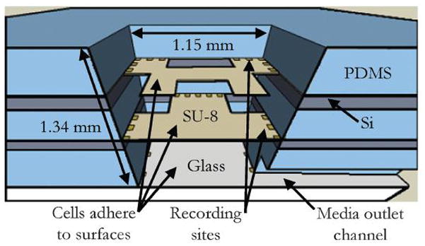
Cross-section of the assembled micro-chamber.
A PDMS ring was constructed by boring an 11 mm diameter hole in a 1 cm thick sheet of PDMS and subsequently using a scalpel to create the ring structure. After all layers had been stacked and bonded, the device and ring were simultaneously treated with O2 plasma (100 W, 20 s) and brought into contact so that the micro-chamber was approximately centered in the ring. To complete bonding, the device with the PDMS ring was placed on a hotplate with the same heating cycle that was used for bonding all previous layers. The micro-chamber itself served as the inlet for the fluidic channel.
The assembly method described here has clear shortcomings when envisioning the possibility of batch production. This issue is addressed below in the section on future design modifications.
Packaging and interfacing
The silicon layers were designed to allow adequate surface for access to the micro-fluidic outlet. The outlet is accessed with a tube that runs from the syringe to a block (approximately 1 cm thick) of PDMS. The PDMS block allows a tight seal so that media can be steadily removed from the device without leaking. Fluid is replenished through the PDMS ring that surrounds the cell chamber (Fig. 4).
Fig. 4.
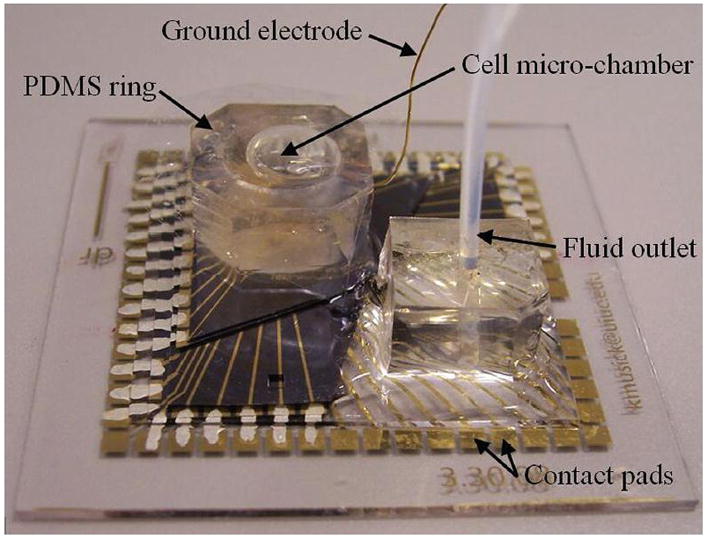
Fully assembled device. For reference, the glass plate is 49 mm × 49 mm.
The bottom electrode layer is glass with contact pads that exactly match the spring-loaded contact pins of the Multichannel Systems M1060 amplifier system. The silicon electrode layers were smaller and subtended only a subset of the contacts. Silver paint was used to connect them to the glass contacts.
As this was a prototype for concept demonstration and mask costs were a constraint, the layout was suboptimal but functional. Improvements would be expected in the micro-fluidic port configuration and the electrical contacts.
Proof-of-concept demonstrations
Introduction
Success of the design approach was demonstrated by the following: (a) biocompatibility demonstrated with cell viability; (b) recording of spontaneous electrical activity from all layers of the device, indicating electrode functionality and nominal cell development; (c) correlated activity from one layer to the next, indicating that multi-level networks had formed; (d) stimulation of the network, including connections from one layer to the next, further demonstrating that 3D networks had been formed and illustrating the utility of the system; and (e) introduction of a drug via the micro-fluidics and monitoring the changes in neural activity, illustrating the potential use for pharmacologic studies.
Biocompatibility
Method of culture
Neurons were cultured with a standard technique [23]. Briefly, embryonic day 18 rat cortical neurons were purchased from BrainBits (www.brainbitsllc.com), dissociated and grown in Neurobasal/B27 medium (Invitrogen, Carlsbad, CA) containing 0.5 mM glutamine. 800 000 cells, suspended in 250 mL, were added to the outer chamber, defined by the PDMS ring shown in Fig. 3. A smaller, unmeasured number fell into the micro-chamber. Alternatively, cells could also be introduced via the micro-fluidic port entering the bottom of the chamber. The devices were then incubated at 37 °C in 5% CO2. Recordings from the cultures were done beginning at 20 days in vitro (DIV).
Constant fluid flow through the device at a rate of 2 mL h−1 was maintained with a syringe pump in order to prevent cell death due to lack of nutrients or buildup of toxins. The volume of the cell chamber is approximately 1.8 mL, which yields a complete micro-chamber media turnover rate of once every 54 min. The media moves from the large PDMS ring through the device and out through the underlying micro-channel. No experiments displayed blockages or impeded flow from detached cells or other debris. Fresh media (100 mL, once every two days for the length of the experiment) is added directly to the large PDMS ring to replenish the lost media.
Cells were visually inspected with transmitting light microscopy to ascertain neurite outgrowth and general health. As the light must pass through the three layers of the device, the clarity of the images is limited.
Results
Under these culturing conditions, neurons survived in the device for more than 28 DIV. A culture at 18 DIV with live cells and good neural outgrowth is shown in detail in Fig. 5. The images were taken with a transmitted light microscope. As the light must travel through all three layers, the image quality is limited. Even with these limitations, neural processes and thick axon bundles can be seen.
Fig. 5.
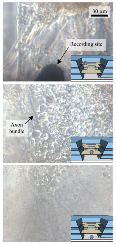
Micrographs of the three layers of the device with cells cultured at 18 DIV. The insets are cross-section of the cell chamber and show the imaging location for each micrograph. The scale is the same for all three images.
Spontaneous recordings
Methods
Recordings were performed with the MEA 1060 amplifier system (gain 1200, bandwidth 10–3000 Hz, Multichannel Systems), maintained at 37 °C, with humidified gas mixture (5% CO2, 10% O2, backfilled with N2). A gold wire inserted into the media through the side of the PDMS ring served as the reference electrode, and a Teflon membrane over the chamber prevented contamination and evaporation. Electrical noise was minimized with an aluminum foil Faraday cage.
Continuous digitized (40 kHz) electrode raw data were collected from 58 channels and stored using hardware and software from Multichannel Systems and analyzed in real time or off-line. Signals were filtered (200 Hz highpass) and thresholded (_5.5 times the standard deviation) to detect neural action potentials. Electrodes with spike rates greater than 0.2 Hz were deemed active.
Recording
Spontaneous recordings from a 20 DIV culture are shown in Fig. 6. The raster plot of the spike events shows activity evident on all three layers of the device. Visually, strong synchrony exists within the electrodes on the top layer of the device with the majority of the active electrodes bursting approximately once every 3 s. This pattern is also shared with Channels 32, 61, 62, and 71 of the middle layer. The bottom layer exhibits qualitatively different activity, with less frequent bursts. This difference in activity is likely due to the difference in cell density on the bottom layer. When plating, cells were loaded in from the top. Each layer acted as a filter and removed a portion of the cells from the solution. Therefore, increasingly lower layers contained a smaller number of cells, and thus a smaller number of connections. Improved loading schemes should be sought in future devices to minimize this effect.
Fig. 6.
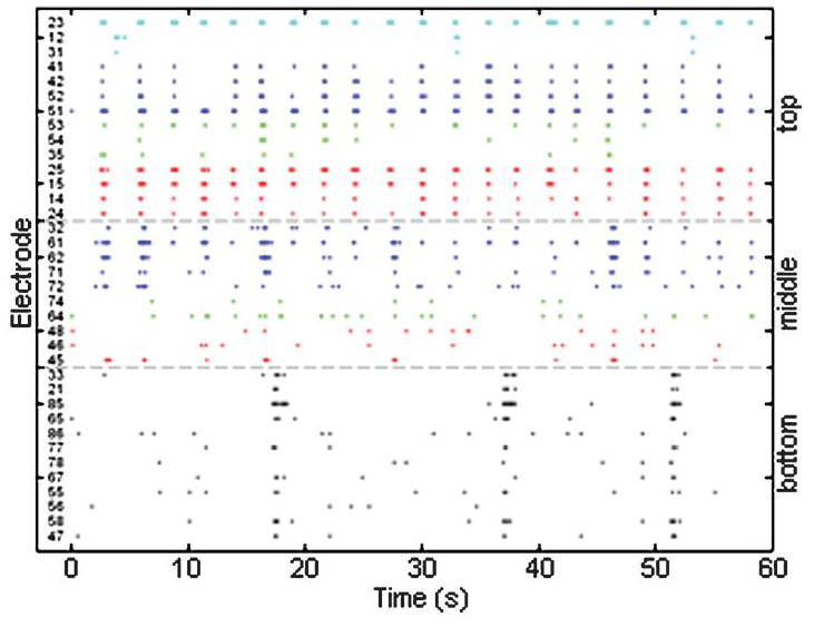
Spike raster plot for one device at 20 DIV. Each dot represents one action potential (spike) and each line depicts the activity from a single electrode. The plot shows widespread activity on all electrodes on all layers. Lines on a layer that are a similar color denote channels that have physical proximity within the device.
Connectivity
To measure possible connectivity, cross-correlograms were calculated. As the most distinctive aspect of this device is the multi-level layout, the most interesting correlations are those between two levels as opposed to correlations within a single level of the device. Fig. 7 shows the cross-correlations of several channels on the top layer and Channel 62 (on the middle layer). The cross-correlograms show peaks before the zero time point, indicating the top channels fire or begin bursting before the channel on the middle layer. The peaks at time values in the range of −300 ms suggest a long and complex functional pathway from the neurons on the top layer to the neuron on the middle layer, with many intermediary neurons along the way. This hypothesis of a long pathway is further supported by the wide standard deviations seen in the cross-correlograms.
Fig. 7.
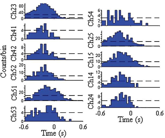
Cross-correlograms of channels on the top layer with Channel 62 (middle layer) as the reference. The dashed lines indicate the 99% confidence level. The peaks before the zero time point imply a causal relationship, where firing on the top level elicits a response from the channel on the middle layer.
Electrical stimulation and evoked responses
Methods
Biphasic voltage pulses, 0.2 ms per phase were delivered directly to the 3D MEA in a monopolar configuration. The pulse train consisted of 10 biphasic voltage pulses, at 1-s intervals, at each level of ±0.6 V, ±0.8 V, ±1.0 V, and ±1.2 V. Each electrode was stimulated in turn to assess activity. Evoked responses were confirmed by plotting the perievent histograms with NeuroExplorer (Nex Technologies, Littleton, MA). Stimulus artifacts lasting up to 7 ms were ignored.
Results
Stimulus/response pairs were recorded from multiple arrays and channels. An example is shown in Fig. 8 where Channel 23 (on the top layer of the device) was stimulated and responses were recorded on Channel 71 (on the middle layer of the device). The spike waveforms recorded on this channel indicate that these events are neural spikes instead of electronic artifacts. The perievent raster plot indicates a connection to the neurons near Channel 23. The data are representative of those needed for network mapping studies.
Fig 8.
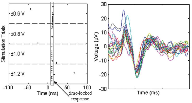
Raster plot from the stimulation trials and corresponding spike waveforms. The stimuli were delivered to Channel 23 (top layer) and the results shown are from Channel 71 (middle layer). Ten stimuli are delivered for each voltage level. The plot shows responses predominantly at 10 ms after the stimulus at t = 0.
Micro-fluidic experiment
Methods
During the multi-week development of the culture in the incubator, a micro-syringe removes media via the fluidic outlet at a fixed rate. In this drug test, done at 20 DIV, the flow was reversed so as to flow through a short (8 cm) piece of tubing. A syringe of fresh media containing 2 mM tetrotodoxin (TTX) was inserted into the tubing with care taken not to introduce any air bubbles. The spontaneous activity was recorded as the drugged media was flowed into the tubing and the chamber at a rate of 120 mL h−1. This rate corresponds to a complete fluid change in the chamber once every 54 s. Flow continued until the TTX media had reached the chamber, which caused a cessation of activity.
The device was then returned to the incubator for 1 h for recovery, with media flow as before (2 mL h−1), and recordings were attempted. Subsequently, media changes were made at one, four and seven days, and recordings at four, seven and eight days.
Results
A culture at 20 DIV that showed good growth on all levels was selected for this experiment. The normalized spike rates of five electrodes as TTX entered the chamber are shown in Fig. 9. The data have been normalized as a fraction of each neuron’s maximum rate. The wash-in effect of the TTX can be clearly seen starting at 17 min and is complete at 20 min, with one electrode showing a burst of activity at 19 min before becoming silent. The time-course for the TTX shown here is comparable to the 2 min reported for the effect of TTX on the Na+ currents in squid giant axons [24].
Fig 9.

Spike rate on five electrodes during the drug experiment (bin = 10 s). The effect of the drug is essentially complete after 19–20 min with a silencing of almost all measurable electrical activity. To better examine the effect of the drug, the spike rates were linearly normalized so that the maximum spike rate on each electrode between 16.5 and 20.5 min was equal to 1.
At 28 DIV (eight days after the drug experiment, but not before) activity resumed on four of the electrodes, indicating recovery of biological function but also that the dose of TTX was higher than optimal for a biological experiment. Nonetheless, the micro-fluidic drug application was shown.
Discussion
This work has demonstrated a layer-by-layer electrode array design concept. The device obtained here is a prototype device with some compromises made for the sake of convenience. The key advantages to this device are modular thin film fabrication, easier packaging, and straightforward interfacing with planaroriented commercial amplifiers. The key disadvantage is the inappropriateness of use with brain slices, a key target application, because they cannot be inserted intact and surround the grid layers in the middle of the chamber.
Future design modifications
There is always a desire to reduce cost and complexity of MEMS designs. Here, the sophisticated processing equipment and materials for the silicon layers dominates the cost. It would be attractive to fabricate the electrodes on a thin polymer, e.g. polyimide, that has been spun on a standard test-grade Si wafer, patterned to have metal electrodes and through-holes, and then lifted off the substrate [25]. Recently, methods for Ti/Au metallization on PDMS have been developed, making this a reasonable avenue for improvement [26]. In our process development we attempted to use polyimide but had difficulties in laminating the fluidics and electrode layers. However, these difficulties might be overcome by others.
The use of self-aligning layers is attractive as it should make routine the accuracy achieved here by hand. By etching identical holes in multiple PDMS films and using surface tension of methanol, stacking and aligning to 15 μm has been shown [22].
Several structural improvements can also be made to this prototype. The width of the grid spanning the chamber could be further optimized to allow the right balance of surface area for cell growth and openness for increased perfusion and neural growth. We used the PDMS layers to insulate the electrodes which greatly accelerated our prototyping. However, the electrode layers should include their own insulation, permitting electrodes to lie within the center of the grids rather than exclusively on the periphery as shown in Fig. 1. Future generations of this device could provide fluidic ports on each layer, permitting more complex fluid control schemes, including the creation and maintenance of concentration gradients within the cell chamber to influence growth direction or cell behavior.
Conclusions
This work is the first demonstration of a design approach for an integrated 3D MEA for 3D neuronal culture. The most notable demonstrations described here are (1) fabrication of the 3D MEA, (2) establishing its electrical functionality with a commercial system, (3) proof of biocompatibility and capability of sustaining long-term in vitro neuronal cultures, (4) acquisition of spontaneous and evoked neural signals, including evidence of true 3D connectivity, and (5) demonstration of the applicability of the device for drug testing and potential for control of chemical gradients for developmental studies. The design strategy is appropriate for a new generation of MEAs.
Acknowledgments
This work was supported in part by National Institutes of Health research grants PHS 1 R01 NS052233 and R01 EB000786.
References
- 1.Dimoka, Courellis SH, Gholmieh GI, Marmarelis VZ, Berger TW. Modeling the nonlinear properties of the in vitro hippocampal perforant path-dentate system using multielectrode array technology. IEEE Trans Biomed Eng. 2008;55:693–702. doi: 10.1109/TBME.2007.908075. [DOI] [PMC free article] [PubMed] [Google Scholar]
- 2.Oka H, Shimono K, Ogawa R, Sugihara H, Taketani M. A new planar multielectrode array for extracellular recording: application to hippocampal acute slice. J Neurosci Methods. 1999;93:61–7. doi: 10.1016/s0165-0270(99)00113-2. [DOI] [PubMed] [Google Scholar]
- 3.Wagenaar DA, Pine J, Potter SM. An extremely rich repertoire of bursting patterns during the development of cortical cultures. BMC Neurosci. 2006:7. doi: 10.1186/1471-2202-7-11. [DOI] [PMC free article] [PubMed] [Google Scholar]
- 4.Gross GW, Rhoades BK, Azzazy HM, Wu MC. The use of neuronal networks on multielectrode arrays as biosensors. Biosens Bioelectron. 1995;10:553–67. doi: 10.1016/0956-5663(95)96931-n. [DOI] [PubMed] [Google Scholar]
- 5.Berthod F, Hayek D, Damour O, Collombel C. Collagen synthesis by fibroblasts cultured within a collagen sponge. Biomaterials. 1993;14:749–54. doi: 10.1016/0142-9612(93)90039-5. [DOI] [PubMed] [Google Scholar]
- 6.Hoffman RM. To do tissue culture in two or three dimensions? That is the question. Stem Cells. 1993;11:105–11. doi: 10.1002/stem.5530110205. [DOI] [PubMed] [Google Scholar]
- 7.Wang F, Weaver VM, Petersen OW, Larabell CA, Dedhar S, Briand P, Lupu R, Bissell MJ. Reciprocal interactions between beta1-integrin and epidermal growth factor receptor in three-dimensional basement membrane breast cultures: a different perspective in epithelial biology. Proc Natl Acad Sci U S A. 1998;95:14821–6. doi: 10.1073/pnas.95.25.14821. [DOI] [PMC free article] [PubMed] [Google Scholar]
- 8.Kloß D, Fischer M, Rothermel A, Simon JC, Robitzki AA. Drug testing on 3D in vitro tissues trapped on a microcavity chip. Lab Chip. 2008;8:879–84. doi: 10.1039/b800394g. [DOI] [PubMed] [Google Scholar]
- 9.Thielecke H, Mack A, Robitzki A. A multicellular spheroidbased sensor for anti-cancer therapeutics. Biosens Bioelectron. 2001;16:261–9. doi: 10.1016/s0956-5663(01)00140-3. [DOI] [PubMed] [Google Scholar]
- 10.Jackson, Fetz EE. Compact Movable Microwire Array for Long-Term Chronic Unit Recording in Cerebral Cortex of Primates. J Neurophysiol. 2007;98:3109–18. doi: 10.1152/jn.00569.2007. [DOI] [PubMed] [Google Scholar]
- 11.Hoogerwerf C, Wise KD. A three-dimensional microelectrode array for chronic neural recording. IEEE Trans Biomed Eng. 1994;41:1136–46. doi: 10.1109/10.335862. [DOI] [PubMed] [Google Scholar]
- 12.Maynard EM, Nordhausen CT, Normann RA. The Utah intracortical electrode array: a recording structure for potential brain-computer interfaces. Electroencephalogr Clin Neurophysiol. 1997;102:228–39. doi: 10.1016/s0013-4694(96)95176-0. [DOI] [PubMed] [Google Scholar]
- 13.Du J, Riedel-Kruse IH, Nawroth JC, Roukes ML, Laurent G, Masmanidis SC. High-resolution three-dimensional extracellular recording of neuronal activity with microfabricated electrode arrays. J Neurophysiol. 2008;101:1671–8. doi: 10.1152/jn.90992.2008. [DOI] [PubMed] [Google Scholar]
- 14.Chu HY, Kuo TY, Chang B, Lu SW, Chiao CC, Fanga W. Design and fabrication of novel three-dimensional multielectrode array using SOI wafer. Sens Actuators, A. 2006;130–131:254–61. [Google Scholar]
- 15.Nam Y, Wheeler BC, Heuschkel MO. Neural recording and stimulation of dissociated hippocampal cultures using microfabricated three-dimensional tip electrode array. J Neurosci Methods. 2006;155:296–9. doi: 10.1016/j.jneumeth.2006.01.014. [DOI] [PubMed] [Google Scholar]
- 16.Heuschkel MO, Fejtl M, Raggenbass M, Bertrand D, Renaud P. A three-dimensional multi-electrode array for multi-site stimulation and recording in acute brain slices. J Neurosci Methods. 2002;114:135–48. doi: 10.1016/s0165-0270(01)00514-3. [DOI] [PubMed] [Google Scholar]
- 17.Irons HR, Cullen DK, Shapiro NP, Lambert NA, Lee RH, LaPlaca MC. Three-dimensional neural constructs: a novel platform for neurophysiological investigation. J Neural Eng. 2008;5:333–41. doi: 10.1088/1741-2560/5/3/006. [DOI] [PubMed] [Google Scholar]
- 18.Choi Y, McClain MA, LaPlaca MC, Frazier AB, Allen MG. Three dimensional MEMS microfluidic perfusion system for thick brain slice cultures. Biomed Microdevices. 2007;9:7–13. doi: 10.1007/s10544-006-9004-8. [DOI] [PubMed] [Google Scholar]
- 19.Rajaraman S, Choi S, Shafer RH, Ross JD, Vukasinovic J, Choi Y, DeWeerth SP, Glezer A, Allen MG. Microfabrication technologies for a coupled three-dimensional microelectrode, microfluidic array. J Micromech Microeng. 2007;17:163–71. [Google Scholar]
- 20.Rowe L, Almasri M, Lee K, Fogleman N, Brewer GJ, Nam Y, Wheeler BC, Vukasinovic J, Glezer A, Frazier AB. Active 3-D microscaffold system with fluid perfusion for culturing in vitro neuronal networks. Lab Chip. 2007;7:475–82. doi: 10.1039/b700795g. [DOI] [PubMed] [Google Scholar]
- 21.Anderson JR, Chiu DT, Jackman RJ, Cherniavskaya O, McDonald JC, Wu H, Whitesides SH, Whitesides GM. Fabrication of topologically complex threedimensional microfluidic systems in PDMS by rapid prototyping. Anal Chem. 2000;72:3158–64. doi: 10.1021/ac9912294. [DOI] [PubMed] [Google Scholar]
- 22.Jo H, Van Lerberghe LM, Motsegood KM, Beebe DJ. Three-dimensional micro-channel fabrication in polydimethylsiloxane (PDMS) elastomer. J Microelectromech Syst. 2000;9:76–81. [Google Scholar]
- 23.Brewer GJ, Torricelli JR, Evege EK, Price PJ. Optimized survival of hippocampal neurons in B27-supplemented neurobasal, a new serum-free medium combination. J Neurosci Res. 1993;35:567–76. doi: 10.1002/jnr.490350513. [DOI] [PubMed] [Google Scholar]
- 24.Cuervo LA, Adelman WJ., Jr Equilibrium and kinetic properties of the interaction between tetrodotoxin and the excitable membrane of the squid giant axon. J Gen Physiol. 1970;55:309–35. doi: 10.1085/jgp.55.3.309. [DOI] [PMC free article] [PubMed] [Google Scholar]
- 25.Boppart SA, Wheeler BC, Wallace CS. A flexible perforated microelectrode array for extended neural recordings. IEEE Trans Biomed Eng. 1992;39:37–42. doi: 10.1109/10.108125. [DOI] [PubMed] [Google Scholar]
- 26.Befahy S, Yunus S, Burguet V, Heine J-S, Dague E, Trooters M, Bertrand P. Metallization process for polydimethylsiloxane (PDMS) rubber. Mater Res Soc Symp Proc. 2007:1009. [Google Scholar]