Abstract
A number of modern experiments require simultaneous measurement of charges on multiple channels at > MHz event rates with an accuracy of 100-1000 e− rms. One widely used data processing scheme relies on application of specific integrated circuits enabling multichannel analog peak detection asserted by an external trigger followed by a serial/sparsified readout. Although this configuration minimizes the back end electronics, its counting rate capability is limited by the speed of the serial readout. Recent advances in analog to digital converters and FPGA devices enable fully parallel high speed multichannel data processing with digital peak detection enhanced by finite impulse response filtering. Not only can accurate charge values be obtained at high event rates, but the timing of the event on each channel can also be determined with high accuracy.
We present the concept and first experimental tests of fully parallel 128-channel charge sensitive data processing electronics capable of measuring charges with accuracy of ~1000 e- rms. Our system does not require an external trigger and, in addition to charge values, it provides the event timing with an accuracy of ~1 ns FWHM. One of the possible applications of this system is high resolution position sensitive event counting detectors with microchannel plates combined with cross strip readout. Implementation of fast data acquisition electronics increases the counting rates of those detectors to multi-MHz level, preserving their unique capability of virtually noiseless detection of both position (with accuracy of ~10 μm FWHM) and timing (~1 ns FWHM) of individual particles, including photons, electrons, ions, neutrals, and neutrons.
I. INTRODUCTION
Many state of the art experimental techniques depend on the capabilities of the detection systems, which frequently have to be optimized in terms of their resolution, sensitivity, dark noise and achievable counting rates. Data processing electronics is one of the key components of defining the characteristics of a particular instrument. In this paper we discuss data processing electronics for event counting imaging detectors, and, in particular, improving the counting rates by orders of magnitude while retaining spatial and temporal resolution.
Detectors with microchannel plates (MCPs) are widely used in applications where event counting with both spatial and temporal resolution is required. One of the major drawbacks of the event counting MCP detectors is their limited counting rate capabilities: each event has to be fully processed before the arrival of the next one. High resolution position sensitive detectors with microchannel plates and cross delay line (XDL) readouts [1], for example, have dead time on the scale of about 400ns, thus limiting the counting rates to few hundred KHz at 10% dead time. Pixelated readouts, such as Medipix2 [2] have a large number of independently counting pixels, each with ~1 μs dead time. Therefore the global counting rate of that readout is very high (> GHz) due to the large number of independently operating channels, but the capability to independently time-tag each event at this rate is lost.
The recent development of another high spatial resolution readout, namely cross strip (XS) anode [3]-[5] with parallel data processing electronics [6] enables substantially higher counting rates exceeding several MHz, while still preserving the spatial resolution of ~10 μm rms. However, the timing channel in those detectors was processed independently from the signals defining the 2-dimensional position of an event. The electron cloud amplified by the MCP falls onto the readout anode, which encodes the center of that cloud by a charge division method. The timing signal was obtained from the back electrode of the MCP stack (Fig. 1). The potential of this electrode exhibits a fast positive pulse as the electron cloud leaves the MCP. This signal is amplified by a fast AC coupled amplifier and fed into time-to-digital converter measuring the fine time of the pulse relative to some event trigger, e.g. a synchrotron trigger. The spatial and timing information of the event is combined together by a coincidence logic providing the synchronization of two independent data channels.
Fig. 1.
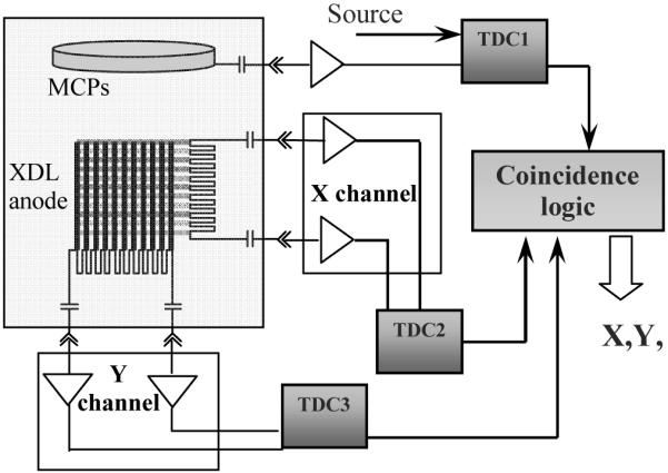
Schematic diagram of previous data processing system for cross delay line detector, which uses 3 time-to-digital converter (TDC) units to provide 2 dimensional position of an event and its timing. The 3 TDC units have to be synchronized through coincidence logic to appropriately match data flows. The timing channel uses the pulse at the back electrode of the MCP stack occurring at the moment when the electron cloud leaves the MCP.
This approach was shown to be very successful for both photon and electron time of flight experiments capable of counting rates of ~0.5 MHz with 10% dead time, spatial resolution ~25 μm and temporal resolution better than 60 ps rms [7]-[9]. However, synchronization of timing and spatial data channels becomes difficult when events pile up and may become a challenging problem for the applications with very high counting rates. Some of the possible solutions to the event pile up problem are the techniques suggested in references [10],[11] and successfully used in a number of multiparticle detection experiments [12],[13]. Distinguishing which XY position belongs to which time can be done by post-experiment sorting the data. In the case of delay line readout the fact that the delay of X and Y lines is a constant allows accurate selection of XY pairs and their time of arrival on the anode [10], or a simultaneous event detection with a CCD camera may allow separation of the events [11]. However, these techniques have not yet achieved the spatial resolution below 10 μm enabling event counting detectors with up to 10000×10000 virtual pixels, as it was shown with novel XS readouts combined with microchannel plates [4],[5].
In this paper we describe the principle of simultaneous XS position and timing data processing and present the first experimental measurements of achievable timing resolution with the current generation of data processing electronics. The new fully parallel digital data processing in the XS detectors [6] allows combining both timing and spatial channels in one data flow and will not need any extra synchronization. This will be beneficial for a number of applications, especially ones which may require processing of several nearly simultaneous events.
II. CROSS STRIP PARALLEL DATA PROCESSING ELECTRONICS
Previous generations of cross strip processing electronics used application specific integrated circuits (ASICs) with analog sample and hold and serial readouts, limiting the count rate to tens of KHz. To overcome this limitation we have designed and tested a new fully parallel system capable of simultaneous detection of charges on all 128 channels [6],[14]. The signal from each electrode of the XS anode is preamplified by one of a set of 32-channel ASIC preamplifiers (peaking time ~50 ns) and then digitized by one of a set of multichannel ADCs running at 60 MHz rate (Fig. 2) [6]. The amplitude peak of the digitized signal is then found using Xilinx Virtex5 FPGA with finite impulse response filtering and a filter matched to the pulse shape of RD20 preamplifiers [14].
Fig. 2.
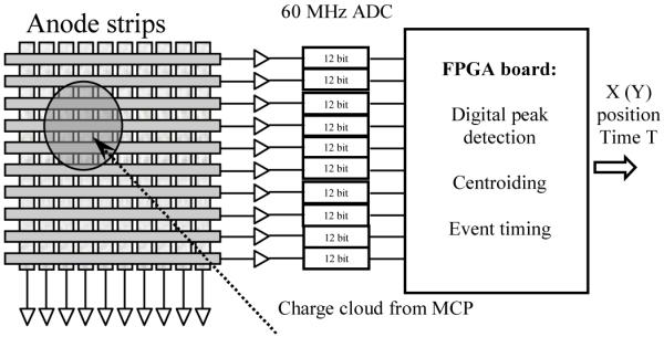
Schematic diagram of the parallel cross strip data processing electronics. Each electrode of the two orthogonal set of fingers is connected to a charge sensitive preamplifier followed by a fast ADC. All digitized channels are fed into Vertex5 FPGA, where an event is detected, peak values are calculated for the electrodes which received charge from MCP cloud followed by the event centroid calculation. The same data is used for calculation of the event timing. Only one set of fingers has its electronics shown.
The present version of event counting detector with microchannel plates and cross strip readout has 32×32 mm2 readout anode with 64×64 fingers, each ~0.5 mm wide. Two sets of orthogonal fingers share (roughly equally) the charge generated by the MCP stack placed ~2 mm above it. The ground layer positioned between the fingers of the orthogonal axes substantially reduces the cross talk between the fingers of the XS anode. A chevron stack of MCPs (33 mm diameter, 80:1 L/D, 13 degree biased microchannels with 10 μm pores on 12 μm centers) was used in the present experiments. All measurements were performed in a vacuum of ~10−6 Torr with UV illumination provided by a mercury vapor penray lamp.
Although the spatial resolution of our previous detector with analog peak detection was shown to be better than the pore diameter (<10 μm) the count rate of that system was limited by very slow shaping time and serial readout. All subsequent events arriving within the time window required for processing were ignored. No simultaneous events could be detected. The new system allows substantially higher counting rates. Moreover, it enables a simultaneous detection of events, which are separated in time by at least one clock cycle (<20 ns) required for the appropriate synchronization of X and Y channels and that do not overlap spatially. The power of field programmable gate arrays (FPGAs) allows accurate digital peak detection of signals from each finger corresponding to the charge received by each electrode, followed by the event centroiding.
The same digitized data can be used to calculate accurate timing for each detected event in the same FPGA providing the spatial information. First, the event timing can be defined as the clock cycle at which the signal reaches its peak, translating to 16.6 ns accuracy for a 60 MHz ADC. However, a factor of ~10 better timing can be obtained by calculating the position of the signal peak within the clock cycle, as shown in the next section.
The current system does not require an external trigger to detect an event: it uses slew detection multiplexed from all the digitized channels with a given threshold to be set above the noise floor (currently ~1000 electrons rms).
III. EXPERIMENTAL RESULTS
It is well known that one of the limiting factors in high counting rate applications with MCPs is the inability of microchannel plates to amplify the signal without gain degradation. The charge produced by a pore or several adjacent pores needs to be replenished before the next event occurs at the same pores. The higher the gain required to operate the detector at a given resolution, the longer the “dead” time of the pore. We have shown that cross strip anodes can sustain high spatial resolution at the detector gains as low as 5×10⁵, almost two order of magnitudes lower than detectors with delay line readouts. Therefore it is the dead time of XS electronics, which determines the counting rate capabilities of the entire detector. The 32-channel RD20 preamplifier ASIC developed previously for other charge sensing applications was found to be well suited to our requirements. Its peaking time is ~50 ns and the signal returns to baseline in ~250 ns (Fig. 3), matching well the speed of multichannel ADCs (markers on Fig. 3) and processing power of Vertex5 FPGA to allow online data processing. The noise of the amplifier is ~1000e rms, which is an acceptable value for our detectors, although less noisier charge amplifiers will allow further reduction of the detector gain and will extend its lifetime.
Fig. 3.
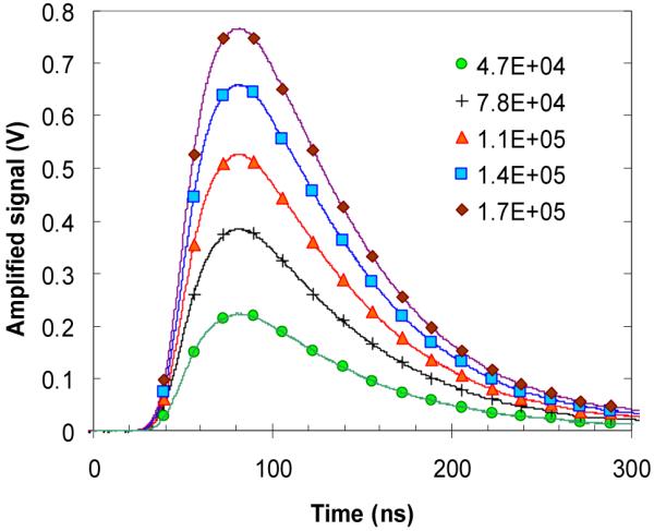
The measured shape of the signals from the charge sensitive multichannel preamplifier board with RD20 ASIC followed by single stage postamplifiers to match the ADC input dynamic range. Signals from only one channel are shown, the others are identical with exception of the pedestal offset, which is corrected in the FPGA data processing. The legend shows the values of the input charges in number of electrons. Solid lines – measured by a 500 MHz digital scope, markers – the values digitized by a 60 MHz ADC.
The digital peak detection in our system is performed with the help of finite impulse response (FIR) filtering: the digitized waveform is convolved with a signal of the same shape. The stability of the shape of the amplified signal is very important for the accuracy of peak detection. Fig. 3 shows the stability of the shape for the input signals varying between 4.7×10⁴ and 1.7×10⁵ electrons. The shape of the pulse remains constant enabling accurate measurement of the charge fallen on each electrode of the XS anode. The gain linearity of the RD20 preamplifiers is shown in Fig. 4 and is taken into account in the charge calculation at the FPGA. The accuracy of the charge detection achieved in our system allows the calculation of the event position with an accuracy ~10 μm for the MCP gains below 106.
Fig. 4.
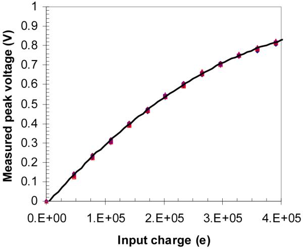
The measured peak voltage at the output of the preamplifier board (input to the ADC) as a function of injected charge. The non-lineariry of the RD20 ASIC preamplifier can be corrected in the FPGA according to this curve.
Calculation of event timing
The timing of the event in our parallel data processing system is performed in two steps: first the clock cycle of the peak value is determined in each channel, followed by calculation of the event temporal “position” with the help of standard constant fraction discriminator (CFD) method [16] - a well known technique to eliminate timing jitter due to variable pulse height. The accuracy of that calculation provides event timing with the accuracy 10 times better than the ADC clock cycle. Fig. 5 shows the digital implementation of the CFD for our particular electronics configuration. The noise of the initial pulse obviously determines the accuracy of the event timing as it will vary the position of zero crossing.
Fig. 5.
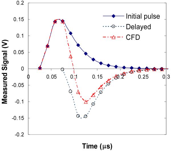
Constant fraction discrimination (CFD) of preamplified signal used for calculation of the event timing. The CFD is used in order to eliminate the influence of the amplitude of the signal on the measured value on time. The zero crossing is calculated from interpolation between two points surrounding x-axis. Markers show the digitized values with 60 MHz ADC, which are used in the digital signal processing.
To evaluate the accuracy achievable in our system we stimulated the XS anode with digital pulse generator (Stanford Research Systems DG535, ~30 ps pulse jitter) with two signals of the same amplitude separated by 1μs and by 1.5 μs, Fig. 6. The amplitude of the signal was varied in order to investigate the amplitude dependence of the achievable time resolution. The calculation of event timing was not fully implemented in the FPGA in these measurements: the digitized raw data was sent to PC where the FIR filtering and digital CFD was performed in order to test the accuracy achievable with our electronics. We do not expect a loss of resolution when the digital filtering and CFD will be transferred into a FPGA as sufficient number of bits can be used for CFD calculations and the resolution of present system is most likely limited by the signal-to-noise ratio.
Fig. 6.
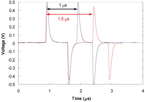
Two input pulses used in calibration of timing resolution. The two pulses separated by 1 and 1.5 μs stimulated the readout electronics to simulate the signals produced by two events separated by a well known time interval. The graphs shows the pulses measured with 500 MHz digital scope. Square pulses generated by a SRS DG535 pulse generator were AC coupled into electrodes of the preamplifier board, resulting in the differential signals shown above, with the positive signals used for the timing experiments.
The histogram of measured time differences between the pulses measured at one individual channel is shown in Fig. 7. The distribution of the measured time intervals is close to a Gaussian with FWHM of ~1 ns. In some cases the accuracy of that timing can be improved by averaging between several channels (each detection event will stimulate ~5 electrodes on each axis of our XS anode). Thus the events separated by at least a few nanoseconds could be easily separated as individual events and appropriately paired for X and Y axes. The requirements on the spatial separation of the events can be slightly relaxed by allowing event pile up, which can be corrected by Maximum Likelihood algorithms, as was already shown in implementation on an FPGA board [17].
Fig. 7.
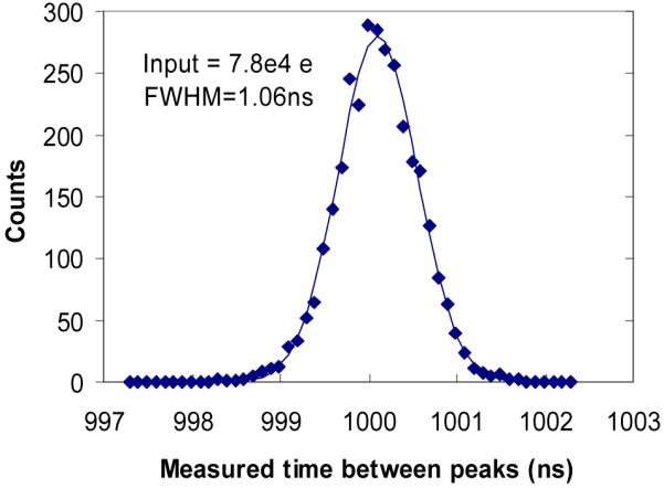
The histogram of measured time intervals between the events generated by a pulse generator, shown in Fig. 6. Distance between the pulses was 1 μs, the input charge into single channel 7.8×10⁴ electrons. The solid line is the Gaussian curve with 1.06 ns FWHM that fit the measured data.
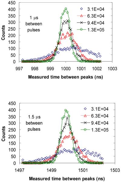
Variation of timing resolution with the amplitude of the input signal is shown in Fig. 8 for input pulses separated by 1 μs and 1.5 μs. The range of input charges was chosen to correspond to the dynamic range of the charges collected by individual electrodes of the anode with detector gain of 2~105 to ~106, sufficient to maintain high spatial resolution. The resolution was found to be very similar for both time ranges at the same input charge, reaching the best value of 0.76 ns FWHM at input charge of 1.3×10⁵ electrons. The higher input charge values cannot be processed by the present electronics due to the limited dynamic range of RD20 ASIC preamplifiers, reaching saturation. The measured timing resolution as a function of input charge is summarized in Fig. 9. The accuracy of event timing decreases rapidly for the input charges below 5×10⁴ electrons. For that reason we have decided to use only one electrode with the largest signal for calculation of the event time, instead of averaging over several fingers stimulated by the electron cloud from the MCP, typically stimulating ~5 fingers with a quasi-Gaussian shape. It is worth noting here that the results of our measurements includes jitter contribution of both pulses, as it will be during data acquisitions measuring time difference between some external trigger (from synchrotron or laser source) and the detected event. The accuracy of that measurement cannot be maintained over very large timing ranges as it is defined by the accuracy of the ADC clock, which is good to 1 part in 106, thus limiting that timing range to below 1 ms if 1 ns accuracy must be maintained.
Fig. 8.
The histogram of measured time intervals between the events generated by a pulse generator. Interval between the pulses was 1 μs (top) and 1.5 μs (bottom). The legend shows the amount of charge injected into a single channel. The same data is obtained in all parallel identical channels of present data acquisition system.
Fig.9.
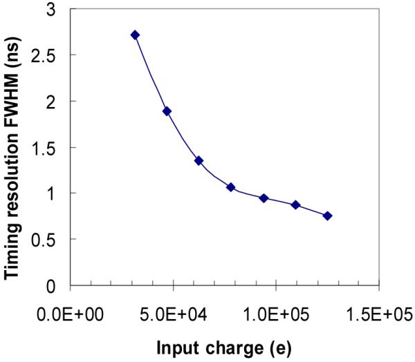
The accuracy of measured event timing as a function of input charge. The large input charges correspond to larger signal to noise values, improving the resolution.
IV. CONCLUSIONS
The self triggered data acquisition system described in this paper uses the same signals for both spatial and timing channels. Although the timing resolution of our new system is not as high as 100ps FWHM achievable with the signal taken from the back end of the microchannel plates, this system has some advantages. First, it does not require an external trigger and produces both spatial and temporal data on each detected event with the same electronics, eliminating the need to synchronize the timing and spatial channels, which can be very challenging for high speed systems. Another attractive feature of the fully parallel system is its high counting rate capability, allowing event overlaps as long as they are separated by more than one clock cycle of analog to digital converter (currently 17 ns) and do not overlap spatially. The rapidly developing technology of fast ADCs and field programmable gate arrays will allow us to improve the resolution of the data processing electronics to even better values. The parallel scheme of data processing also enables the scalability of the system without major redesigning of both hardware and electronics.
The application of more complex parallel electronics obviously makes the data processing units more susceptible to malfunction and radiation damage and increase the power consumption to the level not acceptable for some applications. However, continuous development of new electronics, specifically application specific integrated circuits and radiation hard digital logic may overcome that limitation in the future.
ACKNOWLEDGMENT
The author would like to thank the generous donations of Xilinx FPGAs and programming software tools by the Xilinx University Program of Xilinx, Inc. This work was supported in part by NASA under Grants NNG05GC79G and NNX08AE04G, NSF grant DBI-0552-096 and NIH grant NIBIB R01 EB006353.
Contributor Information
Anton S. Tremsin, Space Sciences Laboratory, UC Berkeley, Berkeley, CA 94720 USA, ast@ssl.berkeley.edu
Oswald H.W. Siegmund, Space Sciences Laboratory, UC Berkeley, Berkeley, CA 94720 USA, ossy@ssl.berkeley.edu
John V. Vallerga, Space Sciences Laboratory, UC Berkeley, Berkeley, CA 94720 USA, jvv@ssl.berkeley.edu
Rick Raffanti, Sensor Sciences LLC, Pleasant Hill, CA 94523, rikraf@earthlink.net.
Shimon Weiss, Department of Chemistry & Biochemistry, University of California, Los Angeles, 607 Charles E. Young Drive East Los Angeles, CA 90095 USA, michalet@chem.ucla.edu.
Xavier Michalet, Department of Chemistry & Biochemistry, University of California, Los Angeles, 607 Charles E. Young Drive East Los Angeles, CA 90095 USA, sweiss@chem.ucla.edu.
REFERENCES
- [1].Siegmund OHW, Jelinsky P, Jelinsky S, Stock J, Hull J, Doliber D, Zaninovich J, Tremsin AS, Kromer K. High resolution cross delay line detectors for the GALEX mission. Proc. SPIE. 1999;3765:429–440. [Google Scholar]
- [2].Llopart X, Campbell M, Dinapoli R, San Segundo D, Pernigotti E. Medipix2, a 64k pixel readout chip with 55 μm square elements working in single photon counting mode. IEEE Trans. Nucl. Sci. 2002;49:2279. Also http://medipix.web.cern.ch/MEDIPIX/
- [3].Siegmund OHW, Tremsin AS, Vallerga JV. High Performance Cross-Strip Detector Technologies; Proc. IEEE Nuclear Science Symposium; 2007; pp. 2246–2251. ISBN: 1-4244-0923-3. [Google Scholar]
- [4].Siegmund OHW, Tremsin AS, Vallerga JV, Abiad R, Hull J. High resolution cross strip anodes for photon counting detectors. Nucl. Instr. Meth. A. 2003;504:177–181. [Google Scholar]
- [5].Tremsin AS, Siegmund OHW, Vallerga JV, Hull J. Cross Strip Readouts for Photon Counting Detectors with High Spatial and Temporal Resolution. IEEE Trans. Nucl. Sci. 2004;51(N4):1707–1711. [Google Scholar]
- [6].Tremsin AS, Siegmund OHW, Vallerga JV, Hull JS. In: Dorn Holland., editor. Novel high resolution readout for UV and X-ray photon counting detectors with microchannel plates; Proc. SPIE 6276, 627616 “High Energy, Optical, and Infrared Detectors for Astronomy II”; Orlando, Florida. May 2006. [Google Scholar]
- [7].Tremsin AS, Siegmund OHW, Hull JS, Vallerga JV, McPhate JB, Soderstrom J, Chiou JW, Guo J-H, Hussain Z. High Resolution Photon Counting Detection System for Advanced Inelastic X-Ray Scattering Studies. IEEE Trans. Nucl. Sci. 2007;54:706–709. [Google Scholar]
- [8].Tremsin AS, Lebedev GV, Siegmund OHW, Vallerga JV, Hull JS, McPhate JB, Jozwiak C, Chen Y, Guo JH, Shen ZX, Hussain Z. High spatial and temporal resolution photon/electron counting detector for synchrotron radiation research. Nucl. Instr. Meth. A. 2007;580:853–857. [Google Scholar]
- [9].Vredenborg A, Roeterdink W,G, Janssen Maurice H. M. A photoelectron-photoion coincidence imaging apparatus for femtosecond time-resolved molecular dynamics with electron time-of-flight resolution of σ=18 ps and energy resolution ΔE/E=3.5% Rev. Sci. Instr. 2008;79:063108. doi: 10.1063/1.2949142. [DOI] [PubMed] [Google Scholar]
- [10].Jagutzki O, Cerezo A, Czasch A, Dörner R, Hattaß M, Huang M, et al. Multiple hit readout of a microchannel plate detector with a three-layer delay-line anode. IEEE Trans. Nucl. Sci. 2002;49:2477–2483. [Google Scholar]
- [11].Ismail IM, Barat M, Brenot J-C, Fayeton JA, Lepère V, Picard YJ. A zero dead-time, multihit, time and position sensitive detector based on micro-channel plates. Rev. Sci. Instr. 2005;76:043304. [Google Scholar]
- [12].Foucar L, Czasch A, Jagutzki O, et al. Multifragment imaging using transient recorder technique. J. Electron Spectroscopy and Related Phenomena. 2007;156:XXXVII–XXXVIII. [Google Scholar]
- [13].Schmidt-Bocking H, Schoffler MS, Jahnke T, et al. Many-particle fragmentation processes in atomic and molecular physics - new insight into the world of correlation. Nucl. Instr. Meth. B. 2005;233:3–11. T. [Google Scholar]
- [14].Van Trees HL. Detection, estimation, and modulation theory. J. Wiley; New York: 1968. [Google Scholar]
- [15].Siegmund OHW, Vallerga JV, Tremsin AS, Weiss S, Michale X. Microchannel Plate Cross-Strip Detectors with High Spatial and Temporal Resolution; 5th International Conference on New Developments In Photodetection; Aix-les-Bains, France. June 15-20, 2008; to be submitted to Nucl. Instr. Meth. A. [DOI] [PMC free article] [PubMed] [Google Scholar]
- [16].Leroux J-D, Martin J-P, Rouleau D, Pepin CM, Cadorette J, Fontaine R, Lecomte R. Nuclear Science Symposium Conference Record, 2004 IEEE Volume 4. Vol. 4. Oct 16-22, 2004. Time discrimination techniques using artificial neural networks for positron emission tomography; pp. 2301–2305. Digital Object Identifier 10.1109/NSSMIC.2004.1462719. [Google Scholar]
- [17].Scoullar Paul A. B., et al. Optimal Digital Pulse Processing for Radiation Detection Systems; proceedings of SORMA WEST 2008 - Symposium on Radiation Measurements and Applications; Berkeley, CA. June 2008. [Google Scholar]


