

Abstract
Piezoresistive sensors are among the earliest micromachined silicon devices. The need for smaller, less expensive, higher performance sensors helped drive early micromachining technology, a precursor to microsystems or microelectromechanical systems (MEMS). The effect of stress on doped silicon and germanium has been known since the work of Smith at Bell Laboratories in 1954. Since then, researchers have extensively reported on microscale, piezoresistive strain gauges, pressure sensors, accelerometers, and cantilever force/displacement sensors, including many commercially successful devices. In this paper, we review the history of piezoresistance, its physics and related fabrication techniques. We also discuss electrical noise in piezoresistors, device examples and design considerations, and alternative materials. This paper provides a comprehensive overview of integrated piezoresistor technology with an introduction to the physics of piezoresistivity, process and material selection and design guidance useful to researchers and device engineers.
Keywords: MEMS, microfabrication, micromachining, micro-sensors, piezoresistance, piezoresistor, sensors
I. INTRODUCTION
Piezoresistive sensors are among the first Micro-Electro-Mechanical-Systems (MEMS) devices and comprise a substantial market share of MEMS sensors in the market today [1], [2]. Silicon piezoresistance has been widely used for various sensors including pressure sensors, accelerometers, cantilever force sensors, inertial sensors, and strain gauges. This paper reviews the background of semiconductor piezoresistor research (Section I), physics and limitations (Section II), applications and devices (Section III), and newer promising piezoresistive materials (Section IV).
A. History
William Thomson (Lord Kelvin) first reported on the change in resistance with elongation in iron and copper in 1856 [3]. Telegraph wire signal propagation changes and time-related conductivity changes, nuisances to telegraph companies, motivated further observations of conductivity under strain. In his classic Bakerian lecture to the Royal Society of London, Kelvin reported an elegant experiment where joined, parallel lengths of copper and iron wires were stretched with a weight and the difference in their resistance change was measured with a modified Wheatstone bridge. Kelvin determined that, since the elongation was the same for both wires, “the effect observed depends truly on variations in their conductivities.” Observation of these differences was remarkable, given the precision of available instrumentation.
Motivated by Lord Kelvin’s work, Tomlinson confirmed this strain-induced change in conductivity and made measurements of temperature and direction dependent elasticity and conductivity of metals under varied orientations of mechanical loads and electrical currents (Fig. 1) [4], [5].
Fig. 1.

The alteration of specific resistance produced in different metals by hammering-induced strain. After Tomlinson, 1883 [5]. Reprinted with permission from the Royal Society Publishing.
The steady state displacement measurement techniques of Thomson and Tomlinson were replicated, refined, and applied to other polycrystalline and amorphous conductors by several researchers [6]–[9]. In 1930, Rolnick presented a dynamic technique to quantify the resistance change in vibrating wires of 15 different metals [10]. In 1932, Allen presented the first measurements of direction-dependent conductivity with strain in single crystals of bismuth, antimony, cadmium, zinc and tin [11]–[14]. Based on her work, Bridgman developed a tensor formulation for the general case of homogeneous mechanical stress on the electrical resistance of single crystals [6], [7].
In 1935, Cookson first applied the term piezoresistance to the change in conductivity with stress, as distinct from the total fractional change of resistance [15]. The term was most likely coined after piezoelectricity, the generation of charge with applied stress, a ferroelectric-mediated effect quite different from piezoresistivity. Hanke coined the term piezoelectricity in 1881 after ‘piezen’ from the Greek to press [16], [17]. The now standard notation for piezoresistivity was adapted from analogous work on piezoelectricity [18]. Voigt formalized tensor notation for stress and strain in crystals and formulated tensor expressions for generalized Hooke’s Law and piezoelectricity [19]. He adapted this notation from the works of Curie and Kelvin [18], [20]–[23].
In 1938, more than 80 years after the discovery of piezoresistance, Clark and Datwyler used a bonded wire to monitor strain in a stressed member [24]. In the same year, Arthur Ruge independently reinvented the bonded metallic strain gauge which had been first suggested by Edward Simmons, Jr. in 1936 [25]–[28].
In 1950, Bardeen and Shockley predicted relatively large conductivity changes with deformation in single crystal semiconductors [29]. In his seminal paper on semiconductor piezoresistance, C. S. Smith (a researcher who was visiting Bell Laboratories from Case Western Reserve University and who was interested in anisotropic electrical properties of materials), reported the first measurements of the ‘exceptionally large’ piezoresistive shear coefficient in silicon and germanium [30].
In 1957, Mason and Thurston first reported silicon strain gauges for measuring displacement, force, and torque [31]. Semiconductor strain gauges, with sensitivity more than fifty times higher than conventional metal strain gauges, were considered a leap forward in sensing technology. Early silicon strain gauges were fabricated by sawing and chemical etching to form a ‘bar’ shaped strain gauge [32]. The gage was then attached to a material surface with cement. This method allowed the development of the first bonded semiconductor pressure sensors. The first commercial piezoresistive silicon strain gauges and pressure sensors started to appear in the late 1950’s. Kulite Semiconductor, founded in 1958 to exploit piezoresistive technology, became the first licensee under the Bell piezoresistive patents [33]. By 1960 there were at least two commercial suppliers of bulk silicon strain gauges: Kulite-Bytrex and Microsystems [33]. Fig. 2 shows modern bar and U-shaped silicon strain gauges.
Fig. 2.
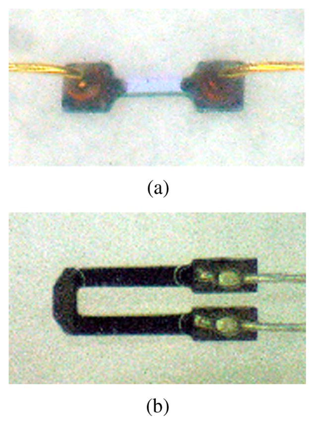
Modern micromachined, precision-etched silicon gages with welded lead wires. (a) Bar shaped strain gauge with a length of 6 mm. (b) U-shaped strain gauge with a length of 1.2 mm. Courtesy of Herb Chelner, Micron Instruments, Simi Valley, CA.
Developments in the manufacture of semiconductors, especially Hoerni’s invention of the ‘planar’ transistor in 1959, resulted in improved methods of manufacturing piezoresistive sensors [34]. Silicon piezoresistive devices evolved from bonded single strain gauges to sensing devices with “integrated” (in the sense that the piezoresistive region was co-fabricated with the force collector) piezoresistive regions. In their classic 1961 paper, Pfann and Thurston proposed the integration of diffused piezoresistive elements with a silicon force collecting element [35]. The first such ‘integrated’ device, a diffused piezoresistive pressure sensing diaphragm was realized by Tufte et al. at Honeywell Research in 1962 [36].
Piezoresistive sensors were the first commercial devices requiring three-dimensional micromachining of silicon. Consequently, this technology was a singularly important precursor to the MEMS technology that emerged in the 1980’s. In 1982, Petersen’s seminal paper “Silicon as a Mechanical Material” reviewed several micromachined silicon transducers, including piezoresistive devices, and the fabrication processes and techniques used to create them [37]. Petersen’s paper helped drive the growth in innovation and design of micromachined silicon devices over the subsequent years.
The field benefited, to a degree that no other sensor technology has, from developments in silicon processing and modeling for the integrated circuits (IC) industry. Technological advances in the fabrication of ICs including doping, etching, and thin film deposition methods, have allowed significant improvements in piezoresistive device sensitivity, resolution, bandwidth, and miniaturization (Fig. 3). Reviews of advances in MEMS, microstructures, and microsystems are available elsewhere [38], [39].
Fig. 3.

Technological advances in IC fabrication (above the horizontal line) and micromachining (below the horizontal line) [30], [33]–[37], [47], [79], [112], [122], [130], [149], [160], [191], [251], [254], [268], [284], [372]–[384].
II. PIEZORESISTANCE FUNDAMENTALS
The electrical resistance (R) of a homogeneous structure is a function of its dimensions and resistivity (ρ),
| (1) |
where l is length, and a is average cross-sectional area. The change in resistance due to applied stress is a function of geometry and resistivity changes. The cross-sectional area of a bulk material reduces in proportion to the longitudinal strain by its Poisson’s ratio, ν, which for most metals ranges from 0.20 to 0.35. For anisotropic silicon, the effective directional Poisson’s ratio ranges from 0.06 to 0.36 [40], [41]. The isotropic lower and upper limit for ν are −1.0 and 0.5 [42].
The gauge factor (GF) of a strain gauge is defined as
| (2) |
where ε is strain and ΔR/R is fractional resistance change with strain. The change in resistance is due to both the geometric effects (1 + 2ν) and the fractional change in resistivity (Δρ/ρ) of the material with strain [10],
| (3) |
Geometric effects alone provide a GF of approximately 1.4 to 2.0, and the change in resistivity, Δρ/ρ, for a metal is small—on the order of 0.3. However, for silicon and germanium in certain directions, Δρ/ρ is 50–100 times larger than the geometric term. For a semiconductor, elasticity and piezoresistivity are direction-dependent under specified directions of loads (stress, strain) and fields (potentials, currents). This section first reviews notation and then discusses fundamentals of piezoresistivity in semiconductors. We also refer the reader to the comprehensive background on piezoelectricity in Nathan and Baltes [43].
A. Notation
1) Miller Indices and Crystal Structure
Crystals have periodic arrangements of atoms arranged in one of 14 lattice types and complete reviews are available elsewhere [44], [45]. The Miller indices specify crystal planes by n-tuples. A direction index [hkl] denotes a vector normal to a plane described by (hkl), and t represents a family of planes equivalent to (hkl) by symmetry. Angle-bracketed indices, like 〈hkl〉, represent all directions equivalent to [hkl] by symmetry. In a hexagonal crystal, as found in most silicon carbide polytypes, the Bravais-Miller index scheme is commonly adopted where four indices are used to represent the intercept-reciprocals corresponding to the four principal crystal axes (a1, a2, a3, and c). The axes a1, a2, and a3 are on the same plane and 120° apart from one another while c is perpendicular to the a-plane defined by the (a1, a2, a3) triplet.
Crystalline silicon forms a covalently bonded diamond-cubic structure with lattice constant a = 5.43 Å [Fig. 4(a)]. The diamond-cubic structure is equivalent to two interpenetrating face-centered-cubic (FCC) lattices with basis atoms offset by 1/4a in the three orthogonal directions [44]. Silicon’s diamond-cubic lattice is relatively sparse (34% packing density) compared to a regular face-centered-cubic (FCC) lattice (74% packing density). Commonly used wafer surface orientations in micromachining include (100), (111), and (110) [Fig. 4(b)]. Photolithography and etch techniques can create devices in various directions to access desirable material properties. For instance a 〈111〉 oriented piezo-resistor in a (110) plane will have the highest piezoresistive sensitivity in a pressure sensor [46]. More commonly 〈110〉 aligned piezoresistors on (100) wafers are used because of their high equal and opposite longitudinal and transverse piezoresistive coefficients. Directionality of silicon piezoresistive coefficients is discussed in Sections II-A3 and II-D1, and the selection of device orientation with directional dependence is discussed in more detail elsewhere [31], [35], [47], [48].
Fig. 4.

(a) Covalently bonded diamond cubic structure of silicon. (b) Commonly employed crystal planes of silicon, i.e., (100), (110), and (111) planes. Silicon has four covalent bonds and coordinates itself tetrahedrally. The {111} planes, oriented 54.74° from {100} planes, are most densely packed. Mechanical and electrical properties vary greatly with direction, especially between the most dense {111} and the least dense {100} planes.
2) Stress, Strain, and Tensors
To define the state of stress for a unit element (Fig. 5), nine components, σij, must be specified, as in:
| (4) |
Fig. 5.

Nine components, σij, of stress on an infinitesimal unit element. For clarity, stresses on negative faces are not depicted.
The first index i denotes the direction of the applied stress, while j indicates the direction of the force or stress. If i = j, the stress is normal to the specified surface, while i ≠ j indicates a shear stress on face i (Fig. 5). From static equilibrium requirements that forces and moments sum to zero, a stress tensor is always symmetric, that is σij = σji, and thus the stress tensor contains only six independent components. Strain, εij, is also directional. For an isotropic, homogeneous material, stress is related to strain by Hooke’s Law, σ = εE [49].
Although “effective” values of Young’s modulus and Poisson’s ratio for a single direction are often employed for simple loading situations, a tensor is required to fully describe the stiffness of an anisotropic material such as silicon [37], [50], [51]. The stress and strain are related by the elastic stiffness matrix, C, where σij = Cijkl * εkl, or equivalently by the inverse compliance matrix, S, where εij = Sijkl * σkl:
| (5) |
| (6) |
Collapsed notation reduces each pair of subscripts to one number: 11→1, 22→2, 33→3, 23→4, 13→5, 12→6, e.g., σ11 to σ1, ε12 to ε6, c1111 to c11 and s2323 to s44.
3) Piezoresistance
Single crystal germanium and silicon, both of which have a diamond lattice crystal structure, were the first materials widely used as piezoresistors. Smith reported the first measurements of large piezoresistive coefficients in these semiconductor crystals in 1954 noting that work by Bardeen and Shockley, and later Herring, could explain the phenomena [30]. Smith applied Bridgman’s tensor notation [8] in defining the piezoresistive coefficients and geometry of his test configurations (Fig. 6). The piezoresistive coefficients (π) require four subscripts because they relate two second-rank tensors of stress and resistivity. The first subscript refers to the electric field component (measured potential), the second to the current density (current), and the third and fourth to the stress (stress has two directional components). For conciseness, the subscripts of each tensor are also collapsed [31], e.g., π1111 → π11, π1122 → π12, π2323 → π44. Kanda later generalized these relations for a fixed voltage and current orientation (ω) as a function of stress (λ) [47]:
| (7) |
Fig. 6.

Notation for Smith’s test configurations. Configurations A and C measured longitudinal piezoresistance, while configurations B and D provided transverse coefficients. Voltage drops between the electrodes (dotted lines) were measured while uniaxial tensile stress, σ, was applied to the test sample by hanging a weight. The experiments were done in constant-current mode in a light-tight enclosure with controlled temperature (25 ± 1 °C). After Smith [30]. © 1954 American Physical Society, http://www.prola.aps.org/abstract/PR/v94/i1/p42_1.
Smith determined these coefficients for relatively lightly doped silicon and germanium samples with resistivities ranging from 1.5–22.7 Ω-cm, e.g., 7.8 Ω-cm for p-type silicon [30]. Current commercial and research practice uses doping levels several orders of magnitude higher than Smith’s. Higher concentrations have somewhat lower piezoresistive coefficients, but much lower temperature coefficients of resistance and sensitivity. For example, in our laboratory, we regularly use doping levels that result in resistivities in the range of 0.005–0.2 Ω-cm [52]–[57]. Smith measured the piezoresistive coefficients for (100) samples along the 〈100〉 and 〈110〉 crystal directions. Longitudinal and transverse coefficients for the fundamental crystal axes were determined directly. Shear piezoresistive coefficients were inferred. By these measurements and considering the crystal symmetry, Smith fully characterized the piezoresistive tensor of 7.8 Ω-cm silicon as
| (8) |
In another early paper, Mason and Thurston utilized bonded gauges with the most favorable longitudinal orientations to measure displacement, force, and torque [31]. They derived directional coefficients from full formulations relating the electric field, current density, and stress components. They also presented more general formulations for longitudinal ( )and transverse ( ) piezoresistive coefficients for a gauge in an arbitrary crystal direction,
| (9) |
and
| (10) |
where l, m, and n are the direction cosines of the direction associated with or , with respect to the crystallo-graphic axes.
Pfann and Thurston [35] recognized the benefits of using transverse and shear piezoresistance effects in conjunction with longitudinal piezoresistance for devices. Many of their geometries employed a full Wheatstone bridge with two longitudinal and two transverse piezoresistors to increase sensitivity and compensate for resistance changes due to temperature (Sections II-D2 and III-E). Notably, they proposed integrating the piezoresistors with the force collecting structure and discussed the advantages and disadvantages of a number of geometries for various types of measurements. They anticipated most of the geometries widely employed today.
Stress sensitivity in silicon also can be exploited by the pseudo-Hall effect and the piezojunction effect. The pseudo-Hall effect is based on the shear piezoresistive effect, whereby the induced shear stress distorts the potential distribution in a piezoresistive plane. Motorola Semiconductor (now Freescale Semiconductor) used this configuration in a pressure sensor in the 1970s [58] and has continued producing this type of pressure sensor. Doelle et al. and Gieschke et al. reported geometry-based design rules and novel applications for the pseudo-Hall effect piezoresistive plates [59]–[61]. The piezojunction effect is defined as the change in the saturation current of a bipolar transistor or a p-n junction due to mechanical stress [62]. Metal-oxide-semiconductor field effect transistors (MOSFETs) using the piezojunction effect have been demonstrated for small cantilever strain sensing [63]–[65]. The main advantage over conventional piezoresistors lies in reduced power consumption but this trades off with size and circuit complexity [66]. The piezojunction effect is also important to understanding sources of unwanted offset in integrated circuits and sensors [67]–[70].
B. Piezoresistive Theory
The discovery of such large piezoresistive effects demanded a theory of the underlying physics. This section discusses the prevailing theories at the time of Smith’s measurements as well as more recent advances. The theories of semiconductor piezoresistance are grounded in one-dimensional descriptions of electron and hole transport in crystalline structures under strain (potentially extended to three dimensions and to include crystal defects, electric potentials, and temperature effects). The various models require some framework of bandgap energy models, wave mechanics, and quantum effects; the interested reader is referred to [44], [71]–[73] and the references of this section for more information.
At the time of Smith’s piezoresistance measurements, existing theories were based on shifts in bandgap energies. The band structure of diamond (Fig. 7) was first calculated by Kimball in 1935 [74], and that of silicon by Mullaney in 1944 [75]. In 1950, Bardeen and Shockley presented a model for mobility changes in semiconductors subjected to deformation potentials and compared both predicted and measured conductivity changes in the bandgap with dilation [29]. This work served as the basis for later analyses, such as that of Herring [76], [77] and Long [78].
Fig. 7.
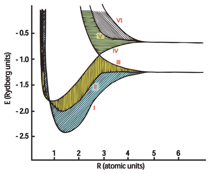
Energy bands split in diamond and are a function of strain or atomic spacing, R (Atomic Units). Besides the four shaded bands, there are four bands of zero width, i.e. two following curve IV and two following curve VI. After Kimball [74]. © 1935 American Institute of Physics.
The mobilities and effective masses of the carriers are significantly different from one another and fluctuate under strain. N- and p-type piezoresistors exhibit opposite trends in resistance change and different direction-dependent magnitudes under stress. The magnitudes and signs of the piezoresistive coefficients depend on a number of factors including impurity concentration, temperature, crystallographic direction, as well as the relation of voltage, current and stress to one another and to the crystallographic axes. The relationship between carrier characteristics and strain has been investigated both experimentally [30], [31], [79] and analytically [29], [35], [47], [77], [80], [81]. Focusing on n-type silicon, these early studies utilized either effective mass or energy band calculations with wave propagation in one direction at a time. The change in mobility (and thus, conductivity) with lattice strain is attributed to band warping or bending and the non-uniform density of states.
The implications for the related large mobility and resistance changes were not realized prior to Smith’s discovery [82], [83]. Following Bardeen and Shockley’s models for mobility changes with deformation potentials, more refined models of transport and energy band structure based on new experimental work became available. In 1955, Herring proposed his Many-Valley model, which adequately explained piezoresistance for n-type silicon and germanium [29], [35], [77], [80], [81], [84]–[87].
Herring’s Many-Valley model for n-type silicon proposes three symmetrical valleys along the 〈100〉 direction [77]. His model projects the band energy minima in three orthogonal directions (x, y, z) as locations of constant minimum energy (Fig. 8). The minimum energy of each valley lies along the centerline of the constant energy ellipsoid of revolution. Electrons have a higher mobility along the direction perpendicular to the long axis of the ellipsoid. Since electrons occupy lower energy states first, they are found in these regions bounded by ellipsoids of constant low-energy. These ellipsoids, bounded by higher-energy regions, are referred to as valleys. With strain however, the symmetry is broken and the ellipsoids are asymmetrically dilated or constricted. This results in an anisotropic change in conductivity proportional to strain.
Fig. 8.

(a, b) Test configuration and resulting schematic diagrams of probable constant energy surfaces in momentum space for n-type Si with potential, E, and strain, e, as depicted. The electrons are located in six energy valleys at the centers of the constant energy ellipses, which are shown greatly enlarged. The effect of stress on the two valley energies shown is indicated by the dotted ellipsoids. The mobilities, μ, of the several groups of charge carriers in various directions are roughly indicated by the arrows. The test configurations correspond to Smith’s experimental arrangements A and C (Fig. 6). After Smith [30]. © 1954 American Physical Society. (c) The changes in silicon energy minima with dilation in a plane normal to a (001) axis. Four minima vary as shown by the solid line, and two on the axis normal to the plane follow the dashed line. After Keyes [87], © 2002 IEEE.
Most models represent the direction dependence of bandgap and electron energies by either directional waves (k has direction and magnitude) or momentum (p) and the effective masses of the carriers. The energy surfaces for electron mobility are accordingly represented in k-space or momentum space. The wave propagation is confined to quantum states by the periodicity of the lattice, and edges in the band diagrams correspond to the edges of the Brillouin zone (smallest primitive cell, or unit cell, of the reciprocal lattice) oriented in a direction of interest [44].
In the unstrained silicon crystal, the lowest conduction band energies (valleys) or highest mobility orientations are aligned with the 〈100〉 directions. The conduction electrons are thus imagined to be lying in six equal groups or valleys, aligned with three 〈100〉 directions. For any valley, the mobility is the lowest when parallel to the valley direction, and the highest when perpendicular to the valley, e.g., an electron in the z valley has higher mobility in the x and y directions. Net electron conductivity is the sum of the conductivity components along the three valley orientations and is independent of direction. Net mobility is the average mobility along the three valleys (two high and one low) [87]. Uniaxial elongation increases the band energy of the valley parallel to the strain and transfers electrons to perpendicular valleys, which also have high mobility along the direction of strain. Electrons favor transport in directions of higher mobility (higher conductivity and lower resistance) in the direction of strain, and tension removes electrons from the valley in that direction and transfers them to valleys normal to the tension. In n-type silicon, average mobility is increased in the direction of tension (longitudinal effect) and lowered transverse to that direction (transverse effect). Compression has the opposite effect. Lin later provided an explanation of large mobility degradation at higher transverse electric fields and lower temperatures based on the physics of electron population and scattering mechanisms of quantized subbands at (100) Si surfaces [88].
The piezoresistance theory for n-type semiconductors continued to be refined from 1954 onward, but until recently “piezoresistive effects in p-type silicon have not been fully clarified due to the complexity of the valence band structure” [89]. In 1993, Ohmura stated that “the [piezoresistance] effect for n-type Ge and Si has been successfully accounted for…” while “the [piezoresistance] effect for p-type Si and Ge has not been fully understood…” [90]. However, recent computational advances have enabled an improved understanding of p-type piezoresistance [73], [91]–[93]. This is important because most research and commercial piezoresistive devices are p-type and models of this successful technology had been largely based on empirical results. Theoretical studies based on the strain Hamiltonian [94]–[96] and on deformation potentials in strained silicon as well as cyclotron resonance experimental results have revealed several factors that affect hole mobilities in semiconductors, e.g., band warping and splitting, mass change, etc. [97]–[101].
Historically, piezoresistive technology drew from mainstream IC research and continues to do so. Now, with the strong interest in “strain engineering” to increase transport speed in ICs, the situation has reversed and mainstream semiconductor technology is drawing on findings of piezoresistive research. Strain engineered materials (e.g., inclusion of germanium into a silicon layer) can increase the mobility of a channel in MOS (metal-oxide-semiconductor) devices [73], [102]–[104]. Suthram et al. [104] applied large uniaxial stress on n-type MOS field-effect transistors (MOSFETs) and showed that piezoresistive coefficients were constant while the electron mobility enhancement increased linearly for stresses up to ~1.5 GPa. Fig. 9 shows plotted hole mobility enhancement factor for several semiconductors as a function of stress.
Fig. 9.

Hole mobility enhancement in semiconductors, taking into account surface roughness scattering, as a function of stress (~GPa). Sun et al. compared their experimental results with those of several groups [385]–[387] and noted that “the hole mobilities of Ge and GaAs increase steadily with stress up to 4 GPa, while the hole mobility of Si saturates at about 2 GPa. For the technologically important stresses of 1–2 GPa, Ge shows similar enhancement as Si. However the unstressed hole mobility of Ge is ~3× higher than Si.” Reprinted with permission from Sun [73], © 2007 American Institute of Physics.
C. Piezoresistor Fabrication
Several design and process parameters such as energy, dose and doping method as well as anneal parameters such as temperature, time and environment affect piezoresistor sensitivity and noise. We review the commonly used fabrication methods for forming piezoresistors on semiconductor substrates and discuss their advantages and drawbacks. Diffusion, ion implantation, and epitaxy are the most common impurity-doping techniques for introducing dopants into a silicon substrate. These techniques result in different doping profiles (Fig. 10). A complete review of doping techniques is available elsewhere [105].
Fig. 10.

(a) Microfabricated piezoresistive cantilever [57]. (b) TSUPREM4 [388] simulation plots of doping profiles using ion implantation vs. epitaxial deposition techniques. Note the difference in the dopant profiles following ion-implantation and epitaxy and the progression of dopant diffusion with increasing time of thermal annealing. Courtesy of Sung-Jin Park, Stanford University.
1) Diffusion
Diffusion is the migration of dopant atoms from a region of high concentration to a region of low concentration. The fabrication of piezoresistors using diffusion involves a pre-deposition and a drive-in step. During the pre-deposition step, wafers may be placed in a high-temperature furnace (900–1300 °C) with a gas-phase or a solid-phase dopant source [105], [106]. The gas-phase dopant source, e.g., diborane (B2H6), phosphine (PH3), or arsine (AsH3), is carried in an inert gas, e.g., N2 or Ar. The solid-phase dopant source (a compound containing dopant atoms in a form of solid discs) is placed such that the active surface is facing the surface of the silicon wafer inside the furnace. Both the source and the wafer are heated, causing transport of dopants from the source to the wafer. Alternately, dopant pre-deposition may utilize doped spin-on glass layers [107]–[109]. During pre-deposition, the boundary condition is a constant surface concentration and the doping profile is approximated by a complementary error function. The source can be removed and dopants “driven-in” deeper with high temperature annealing (900–1300 °C). Gas-phase dopant sources provide inconsistent doses for surface concentrations below the solid solubility level.
2) Ion Implantation
Ion implantation was researched extensively in the 1950s and 1960s as an alternate pre-deposition method to provide better control of the dopant dose [105], [110]–[121]. Ion implantation gained wide use in the 1980s and remains the preferred method today. In ion implantation, dopant ions are accelerated at high energy (keV to MeV) into the substrate. The ions leave a cascade of damage in the crystal structure of the implanted substrate [118]. Any layer thick or dense enough to block the implanted ions, such as photoresist, silicon oxide, silicon nitride, or metal, can be used for masking. Typical silicon piezoresistor doses range from (1 × 10¹⁴ to 5 × 1016 cm−2, with energy ranges from 30 to 150 keV [51]. Dopant distribution is approximated by a symmetric Gaussian distribution (Fig. 10). Most implants are done with a 7° tilt of (100) silicon wafers to avoid ion channeling, a phenomenon where ions deeply traverse gaps in the lattice without scattering. Larger implant angles (7°–45°) are sometimes used to form piezoresistors on etched sidewalls of deep-reactive-ion-etched (DRIE) trenches as found in flexures or beams in dual-axis cantilevers, in-plane accelerometers, and shear stress sensors [53], [122]–[125]. One major disadvantage of ion implantation is significant damage to the crystal. Lattice order is mostly restored by high-temperature dopant activation and annealing [118]. However, shallow junctions are difficult to obtain with high crystal quality. Parameters that affect the junction depth include the acceleration energy, the ion mass, and the stopping power of the material [115].
3) Epitaxy
Epitaxy is the growth of atomic layers on single-crystal materials that conform to the crystal-structure arrangement on the surface of the crystalline substrate [105]. Chemical Vapor Deposition (CVD) technique can be used to deposit epitaxial silicon by decomposing silane (SiH4) or by reacting silicon chloride (SiCl4) with hydrogen. Conventional epitaxial growth is done at high temperatures (1000–1250 °C) and reduced pressure (30–200 torr). A clean surface is necessary to obtain a high quality epitaxial layer. Contaminants and native oxide will prevent single-crystal growth. An in situ HCl clean can remove wafer contaminants and native oxide. Halide source gases, such as SiCl4, SiHCl3, or SiH2Cl2 (DCS), are used to grow silicon with the advantage that chlorine is one of the net byproducts. The chlorine removes metal contaminants from the deposited silicon film, resulting in better quality single-crystal silicon. Selective deposition of epitaxial silicon, i.e., the silicon deposits only on exposed regions of silicon, but not on other dielectric films such as SiO2 or Si3N4, can be achieved by tailoring the deposition conditions [55], [105], [126]–[129]. Epitaxial silicon films may be doped during the deposition by introducing appropriate dopant source gases such as AsH3, PH3, or B2H6 into the chamber along with the silicon source gases.
Epitaxial piezoresistors require no annealing and have a uniform dopant profile (Fig. 10). Epitaxy has enabled ultra thin piezoresistive layers and increased force sensitivity [130]. Harley and Kenny [131] and Liang et al. [132] demonstrated the use of epitaxially grown doped silicon to form piezoresistors in ultra-thin cantilevers (less than 100 nm). This is a practical method for such thin piezoresistive cantilevers, especially given the difficulties of implanting shallow junction depths (less than 50 nm), activating dopant atoms, and restoring lattice quality. Joyce and Baldrey [126] first demonstrated selective deposition of silicon epitaxial layers using oxide-masking techniques in 1962 and Zhang et al. [133] demonstrated an HCl-free selective deposition technique. We have also demonstrated epitaxial piezoresistors on the sidewalls of microstructures for in-plane sensing applications using selective deposition techniques [55]. These epitaxial sidewall piezoresistive sensors showed increased sensitivity over oblique-angle ion-implanted piezoresistors of the same dose.
4) Doped Polysilicon
Polycrystalline silicon (polysilicon or “poly”) may be doped by diffusion, ion implantation, or in situ doping. Polysilicon in situ doping introduces gas-phase dopants with the precursor polysilicon gases during chemical vapor deposition. However, introduction of dopant gases results in non-uniform polysilicon layer thickness across the wafer, a lower deposition rate, and dopant nonuniformity [105]. Moreover, adding dopants during the deposition of the polysilicon layer also affects layer properties and changes grain size, grain orientation, and intrinsic stress. The deposition temperature, anneal time and anneal temperature determine the surface roughness, grain size, grain orientation, and intrinsic stress of the resulting polysilicon layer.
Piezoresistive effects in polysilicon were studied extensively in the 1970s and 1980s [134]–[146]. French and Evans presented a theoretical model for piezoresistance in polysilicon as a function of doping, grain size, and orientation and proposed an optimum set of processing parameters for a given grain size [145].
5) Tradeoffs in Process Selection
Ion implantation is the most common method of fabricating piezoresistors. Advantages of ion implantation include precise control of dopant concentration and depth. Disadvantages include lattice damage and annealing requirements for dopant activation. Diffusion has the advantage of batch processing, but suffers from poor dopant depth and concentration control. Epitaxy provides excellent depth control without annealing, which enables shallow junctions with abrupt dopant profiles. However, processing complexity and equipment costs and availability are drawbacks to epitaxy. Table 1 compares ion-implantation, diffusion, and epitaxy techniques.
Table 1.
Comparisons of Doping Methods (After Plummer et al. [105])
| Ion implantation | Diffusion | Epitaxy | |
|---|---|---|---|
| Process condition | room temperature, vacuum, batch process | high temperature, batch process | high temperature, low pressure, single wafer |
| Damage | significant, requires annealing, enhances diffusion | none | none |
| Doping concentration control | excellent | acceptable | good |
| Dopant depth control | good | not good | very good |
| Typical range of doses or concentration | 1×10¹¹ to 1×1016 cm−2 | concentration is limited to solid solubility | 1×l014 to 1×1017 cm−2 |
| Masking | photoresist or hard mask (silicon oxide, silicon nitride, metal, etc.) | hard mask | oxide mask and selective deposition (more difficult) or etchback |
D. Design and Process Effects on Piezoresistor Performance
Design and process parameters affect piezoresistor sensitivity and noise. Sensitivity is a strong function of dopant concentration and piezoresistor orientation. In choosing the device geometry, doping, and anneal conditions, the piezoresistive device designer must also consider the temperature coefficients of sensitivity and resistance, nonlinearity with strain and temperature, and noise and resolution limits.
1) Device Doping and Orientation
Initial experiments by Smith used bars of silicon cut from wafers doped while growing the single-crystal ingot [30]. Later, Pfann and Thurston [35] suggested diffusion techniques to integrate doped piezoresistors on the sensor surface. The piezoresistive properties of diffused layers were subsequently investigated by Tufte and Stelzer [79]. They also provided empirical data on piezoresistive coefficients for different surface concentrations and resistivities. Kurtz and Gravel replotted their data and noted that the piezoresistive coefficients decrease approximately with the log of surface concentration [147].
The early analyses by Smith, and Pfann and Thurston, covered virtually all crystal orientations and piezoresistor designs for n-type and p-type piezoresistors in use today. Kanda [47] extended these analyses with graphical representations of the piezoresistive coefficients in arbitrary directions in the commonly used (100) crystal plane and the less common (110), and (211) planes. These graphs provide a useful picture of how piezoresistive coefficients vary with respect to crystal orientations for both longitudinal and transverse geometries (Fig. 11). Kanda also presented theoretical calculations of piezoresistive change versus dopant concentration. He suggested a simple power law dependence of the relaxation time with temperature and noted a discrepancy between his calculations and the experimental data for high doping concentrations (Fig. 12). In his notation, the piezoresistive coefficient is calculated by multiplying the piezoresistive factor, P(N, T) (Fig. 13), by the room temperature piezoresistive coefficient. The calculated values of the P(N, T), agree well with the experimental values obtained by Mason [148] for doping concentrations less than 1 × 1017 cm−3, over the temperature range of −50 to 150 °C, but differ by 21% at a concentration of 3 × 1019 cm−3 at room temperature. The error was attributed to dopant ions scattering for high dopant concentrations, whereas the calculation only considered lattice scattering. Harley [149] later evaluated data from several researchers and provided an empirical fit of piezoresistance vs. concentration that better estimates the sensitivity for higher concentration devices. Our devices typically fall in a regime described by extension of Harley’s fit [55]–[57], [150].
Fig. 11.

Room temperature piezoresistive coefficients in the (100) plane of (a) p-type silicon (b) n-type silicon. These graphics predict piezoresistive coefficients very well for low doses. After Kanda [47], © 1982 IEEE.
Fig. 12.

Piezoresistive coefficients as a function of doping. Experimental data obtained by Kerr, Tufte, and Mason are fitted by Harley and Kenny [79], [148], [149], [157]. Theoretical prediction by Kanda overestimates the piezoresistive coefficients at higher concentrations. After Harley and Kenny [149], © 2000 IEEE.
Fig. 13.

The adjusted piezoresistance factor P(N,T) as a function of impurity concentration and temperature for (a) p-type silicon (b) n-type silicon. These graphics predict piezoresistive coefficients very well for low doses but the trends with temperature are correct. After Kanda [47], © 1982 IEEE.
Four-point bending is used to measure piezoresistive effects in semiconductors [151], [152], though care must be taken in high-stress test conditions [104]. Richter et al. [48], [153], [154] demonstrated a novel piezocoefficient-mapping device to measure 3D stresses in device packaging and also to extract directional piezoresistive coefficients (Fig. 14). Using orthogonal 〈100〉 piezoresistors and 4-point bending strain along the 〈110〉 direction, they measured piezoresistance coefficients for silicon and strained silicon (Si0.9Ge0.1) molecular beam epitaxial (MBE) grown layers at boron doping levels of 1 × 10¹⁸ and 1 × 1019 cm−3; they extracted piezoresistive coefficients as a function of doping and direction. Their results are higher than Smith’s lower dose values and also showed that lattice strain raises the value of π44.
Fig. 14.

(a) Stress sensor chip with a p-type circular piezoresistors in the middle of the chip. (b) Schematic diagram of the circular piezoresistor with a radius of 1700 μm. From Richter et al. [154], © 2007 IEEE.
2) Temperature Coefficients of Sensitivity and Resistance
Piezoresistors are sensitive to temperature variation, which changes the mobility and number of carriers, resulting in a change in conductivity (or resistivity) and piezoresistive coefficients (sensitivity) [155]. Consequently, doped silicon can be used for accurate temperature sensing as in resistance temperature detectors (RTDs). A typical commercial piezoresistive pressure sensor has a thermal resistance change ten times the full-scale stressed resistance change over a temperature range of 55 °C. Kurtz [156] presented data and discussed the trend of the piezoresistive coefficient (π), temperature coefficient of piezoresistive coefficient (TCS), resistivity (ρ), temperature coefficient of resistivity (TCR) and strain nonlinearity, as a function of dopant concentration (Fig. 15).
Fig. 15.

Trends of key piezoresistive properties with concentrations, such as (a) longitudinal piezoresistive coefficient (sensitivity) (b) temperature coefficient of sensitivity (c) temperature coefficient of resistivity with dopant concentration. After Kurtz and Gravel [147]. © 1967 Industrial Automation Standards.
Kurtz was the first to clearly highlight the advantages of using higher doping levels for piezoresistors. The temperature dependence of sensitivity decreases with increasing surface concentration. This trend is desirable except that increasing surface concentration also sacrifices the sensitivity of the piezoresistors. However, the temperature coefficient of sensitivity drops off faster than sensitivity. Also at higher doping levels, the strain and temperature nonlinearities in sensitivity, and temperature change of resistance are very much reduced. Some piezoresistive pressure sensor manufacturers, such as Kulite Semiconductor Products, Merit Sensors, and GE NovaSensor manufacture high-dose piezoresistors, taking advantage of this reduced temperature sensitivity. Ultimately some temperature dependence in silicon strain sensors is inevitable though this dependence may be compensated by the use of a half or full-active Wheatstone bridge and conditioning circuitry (Section III-E).
Tufte and Stelzer [79] first presented detailed measurements of these parameters for diffused layers over a wide range of dopant concentrations (1018 – 1021 atoms cm−3) and temperatures (−90 °C to 100 °C). They also showed that the piezoresistive coefficient was relatively insensitive to the diffusion depth for a diffused layer. Kerr and Milnes [157] showed that the surface dopant concentration could be used as an adequate proxy for the average effective concentration in modeling the piezoresistivity of diffused layers. More recently, refined concentration-dependent temperature sensitivity measurements have been reported on integrated die using 4-point bending and finite element analysis of stress profiles [158].
3) Nonlinearity
The response of piezoresistors to stress is nonlinear at larger strain (> 0.1%). Understanding and compensating for the nonlinearity of piezoresistors is important for precision piezoresistive devices. Matsuda et al. [159], [160] calculated and measured the piezoresistive coefficients and third-order effects for both p-type and n-type silicon for the three major crystallographic orientations with strain up to 0.1%. Higher strain levels were difficult to measure since surface defects in the silicon lattice cause fracture at low strain levels. Addressing this problem, Chen and MacDonald [161] co-fabricated a microactuator and a 150-μm-long, 150-nm-diameter single-crystal silicon fiber from one single-crystal silicon substrate to reduce the possibility of defects, allowing measurements of strains greater than 1%. With the increased range of strain, the second and third order fit for piezoresistive coefficients were quantified more accurately (Fig. 16). Table 2 shows the results obtained by Chen and MacDonald compared to the data obtained by Tufte and Stelzer [162]. Additional studies of the effects of strain on semiconductor properties have been undertaken recently as interest in strained substrates has increased [48], [73], [104], [163].
Fig. 16.

(a) SEM image of micro-actuator and 150-μm-long, 150-nm-diameter, phosphorous-doped, 〈110〉 silicon fiber (test sample) with resistivity of 0.6 mΩcm. (b) Percentage change longitudinal piezoresistance vs. strain exhibited less nonlinearity at low strain than previous reports at lower doping (Data of Matsuda et al. [161] were included by converting stress data using Young’s modulus of 170 GPa). Reprinted with permission from Chen and MacDonald [161], © 2004 American Institute of Physics.
Table 2.
Piezoresistive Coefficients Using Data From 0% to 1% Strain. From Chen and MacDonald [161], Reprinted With Permission From American Institute of Physics
| [110] longitudinal piezoresistive coefficients | Piezoresistance of n-type silicon fiber with doping level of 2×1020 cm−3 | Tufte and Stelzer [163] n-type silicon with doping level of 2×1020 cm−3 |
|---|---|---|
| First-order π1(10−4MPa−1) | −1.86 ± 0.01 | −1.9 |
| Second-order π2(10−7MPa−2) | 0.12 ± 0.01 | N/A |
| Third-order π3(10−10MPa−3) | 0.100 ± 0.003 | N/A |
E. Noise in Piezoresistors
Electrical noise is the random variation in the potential of a conductor. The electrical noise in a piezoresistor sets the fundamental lower limit of piezoresistive transducer resolution. The dominant random electrical noise sources in piezoresistors are Johnson (thermal) noise and 1/f (flicker) noise. Other noise sources, such as inductive or capacitive line pickup also exist [51]. Also, for many applications the accuracy of piezoresistive transducers is limited by temperature effects or thermo-mechanical hysteresis, e.g., in commercial piezoresistive devices such as piezoresistive pressure sensors. Integrated shield layers have been shown to reduce noise effects, including temperature sensitivity [164].
1) Thermal Noise
Thermal noise, also known as Johnson or Johnson-Nyquist noise, is universal to resistors. It was first observed in 1928 by Johnson [164] and theoretically explained by Nyquist [165]. Thermal noise is a function of the absolute temperature T(K) of the resistor, resistance value R(Ω), and Boltzmann’s constant k (J/K). For a 1 Hz bandwidth the thermal noise is:
| (11) |
Thermal noise is fundamental, exists in all resistors, and cannot be eliminated. A discussion on thermal noise in modern devices can be found elsewhere [166].
2) 1/f Noise
The power spectral density of 1/f noise, as its name implies, is inversely proportional to frequency. The origins of 1/f noise are still not fully understood and remain an active topic of research [167]–[178]. In particular, 1/f noise in piezoresistors is dependent on fabrication process parameters, such as implant dose and energy, and anneal parameters. A 1/fn noise exponent of n >1 can be a measure of conductor reliability. Excessive 1/f noise can indicate poor fabrication process quality [179], [180]. Several researchers have presented piezoresistive device optimization to include 1/f noise [149], [181]–[183].
Despite many decades of research, the source of 1/f noise is still debated [176]. McWhorter and Hooge proposed two opposing theories of 1/f noise. These views are currently the leading explanations for the origin of 1/f noise. The McWhorter model attributes the 1/f noise to surface factors [184], [185], while the Hooge model implicates bulk defects [167], [177] (Fig. 17).
Fig. 17.
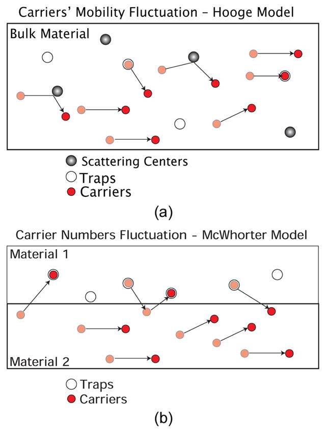
Conductivity fluctuations based on (a) Hooge model (bulk effect) (b) McWhorter model (surface effect). Courtesy of Paul Lim, Stanford University.
Experiments show that 1/f noise is due to conductivity fluctuations in the resistor [177], [178]. Hooge showed that the 1/f low-frequency noise modulated the thermal noise even with no current flowing through the resistor [172]. This experiment demonstrates that 1/f noise is not current-generated. Current is only needed to transform the conductivity fluctuations into voltage fluctuations. Thermal and 1/f noise are fundamentally different. Thermal noise is a voltage noise; therefore it does not depend on the amount of current in the resistor. In contrast, 1/f noise is a conductivity noise; therefore the voltage noise is proportional to the current in the resistor.
Hooge’s empirical 1/f noise model, fit to observed data, predicts that the voltage noise density is given by:
| (12) |
where f, N, and Vb, are frequency, total number of carriers in the resistor volume, and bias voltage across the resistor, respectively. A non-dimensional fitting parameter, α, is ascribed to the “quality of the lattice” and typically ranges from 10−3 down to 10−7 [56], [149], [183].
Attempts to observe the lower limit of 1/f, below which the spectrum theoretically flattens, have not been successful [177]. Measurements down to 3 μHz (or approximately 4 days per cycle) show a noise spectrum that is still 1/f [186]. Harley and Kenny showed that resistors with different surface to volume ratios have the same 1/f noise characteristics, and 1/f noise scales with the resistor volume, consistent with Hooge’s empirical equation [149].
Hooge defines 1/f noise as only those spectra with a frequency exponent of 0.9–1.1. Noise with a different power spectral density and other frequency exponents, sometimes referred to as 1/f-like noise, is often confused with 1/f noise and is not predicted by the Hooge equation. According to Hooge, noise with a higher exponent, e.g., 1.5 or 2, indicates noise mechanisms other than mobility fluctuations that should not be considered 1/f noise and are not predicted by (12). Abnormal 1/f noise characterization can give insights into piezoresistor reliability and failure analyses. For example, Neri [187] found that the 1/f exponent is closer to 2 in metal traces that exhibit electromigration. Vandamme [188] showed that excess 1/f noise in semiconductors can be attributed to small constrictions and current crowding. Devices with constriction resistance show third harmonics and nonlinearities in their output.
Current crowding theory also explains why polysilicon has higher 1/f noise than its crystalline counterpart [168]. At grain boundaries, small constrictions are present, thus reducing the total number of carriers (N) and effectively increasing the 1/f noise. Basically, 1/f voltage noise does increase linearly with the applied excitation. If the noise spectrum trends otherwise, then other mechanisms, such as current crowding, could be present. The noise floor of the experimental setup may be verified by reducing the applied excitation and observing only the thermal noise of the piezoresistor.
Reducing 1/f noise is important for low frequency applications. Chemical and bio-sensing applications based on displacement transduction require static and low frequency measurements and require stability over time periods of tens of seconds to many hours. Lower 1/f-noise piezoresistors are required for these applications. The fabrication process parameters can be tailored to achieve low 1/f noise amplitude spectral densities. As suggested by Kanda’s model, low impurity doping is often used to achieve high sensitivity. However, this model underestimates sensitivity at high and low doping and leads to a device design that poorly trades-off sensitivity with noise for lower frequency applications. The empirical data of Tufte and Seltzer [79], on the other hand, offer better guidance in these regimes. The advantages of high doping are lower noise and lower temperature coefficients for modest reduction of sensitivity. For example, if peak doping concentration, Cpeak, decreases from 1019 cm−3 to 1017 cm−3, the sensitivity increases by only 65% while the noise increases by a factor of ten. From (12), the 1/f noise can be reduced by increasing N, the total number of carriers dependent on piezoresistor volume and impurity implant dose, and reducing α. Vandamme [179], [189] showed that α depends on crystal lattice perfection and lattice quality increases with higher temperature anneals and longer anneal times. Mallon et al. [56] extended the work of Harley and Kenny [56], [149] and showed that long, high temperature anneals can produce lower noise piezoresistors with low values of α (Fig. 18).
Fig. 18.

Hooge noise parameter, α, improves (decreases) with increasing anneal diffusion length, √Dt. Reprinted with permission from Mallon et al. [56]. © 2008 American Institute of Physics.
Fig. 19 shows the typical 1/f noise of a piezoresistor. The horizontal straight line is the thermal noise of the resistor. For reference, a 1 kΩ resistor has 4 nV/√Hz thermal noise; other resistor values are easily referenced to this value. The thermal noise of a resistor is also an excellent source to calibrate and verify the measurement system [190]. The straight, sloped line is the 1/f noise of the resistor, which depends on the applied bias voltage. If the resistor is unbiased, the 1/f noise disappears, while the thermal noise remains. The 1/f noise is proportional to applied bias voltage with proportionality constant . The total noise is the sum of thermal and 1/f noise. Since the noise sources are uncorrelated they are additive as,
Fig. 19.

Typical noise curve of a full-bridged piezoresistor. The sloped solid line is the total noise dominated by 1/f-noise component, while the horizontal solid line is the total noise dominated by thermal-noise component. The 1/f noise corner frequency is the frequency at which the thermal noise is equal to the 1/f noise. In this noise spectrum, the corner frequency is ~1 Hz. The horizontal dashed line is the measurement system noise level, which is verified with a 680 Ω resistor from 0.01 Hz. For clarity, system noise is not shown above 1 Hz. The noise is measured using modulation-demodulation technique (Section III-E). The roll-off above 60 Hz is due to system bandwidth. Reprinted with permission from Mallon et al. [56]. © 2008 American Institute of Physics.
| (13) |
III. DEVICES AND APPLICATIONS
Piezoresistors are widely used in pressure, force and inertial sensors. An external force creates a deflection or stretch in the structure proportional to the measurand, and piezoresistance varies proportional to the applied stress. When used in a Wheatstone bridge or other conditioning circuit, the change in resistance is converted to change in voltage output. In this section, we review some of the most commonly used devices that employ piezoresistive transduction schemes in microsystems as well as common signal conditioning approaches. For brevity we focus on seminal and representative examples of the art.
A. Cantilever Sensors
Cantilevers are beams with one free and one fixed end (Fig. 20). A piezoresistive cantilever force sensor normally has a piezoresistor at the root of the beam, near the top surface to maximize sensitivity. From beam mechanics, the maximum stress (σ) occurs at the outer surface of the root (y = ±h/2, x = 0), when an external force (F) is applied at the end of a cantilever (x = L):
| (14) |
where x is the distance along the length of the cantilever measured from the root, y is the distance along the thickness of the cantilever measured from the neutral axis, b is the width, and h is the thickness of the cantilever.
Fig. 20.

A cantilever with applied force at the tip and the resulting stress profile in the beam. The maximum stress occurs at outer surface of the root (y = ±h/2, x = 0).
The change in resistance is a function of the stress in the piezoresistor. The cantilever is a ubiquitous structure in the field of micromachined transducers. Cantilevers are relatively simple and inexpensive to fabricate, and analytical solutions of displacement profiles and stress distributions under load are well developed [49]. Cantilever beams are commonly used as force and displacement sensors as well as mass sensors when excited in resonance. Various schemes can transduce the force applied to the cantilever by measuring the stress (piezoresistive) or displacement (optical, capacitive) at any location on the cantilever.
The earliest work on integrated silicon piezoresistive cantilevers started in the late 1960s, when Wilfinger [191] used a silicon cantilever with diffused piezoresistive elements as a ‘resonistor’ (resonator). The silicon cantilever was mechanically deflected by electrically induced thermal expansion. The piezoresistors were used to detect the maximum stress at the resonant frequency. Fulkerson [192] integrated a bridge and an amplifier circuit in a microfabricated piezoresistive cantilever sensor to linearize and amplify the output, pioneering the concept of signal conditioning integration. Numerous resonant, piezoresistive cantilever devices have been implemented for mass sensing, chemical sensing, and inertial sensing since that time [193]–[195].
Perhaps the best-known application of cantilevers as force and displacement sensors is in Atomic Force Microscopy (AFM). AFM was invented by Binnig, Quate, and Gerber in 1986 as the first tool capable of investigating the surface of both conductors and insulators at the atomic scale [196]. The first AFM combined Scanning Tunneling Microscopy (STM) technology [197] and a stylus profilometer. This AFM used tunneling current for cantilever displacement detection and achieved lateral and vertical resolutions of 30 Å and less than 1 Å, respectively. Since then, other detection methods such as optical [198] and capacitive [199], [200], have been used to detect the displacement of the AFM cantilever. However, these methods require a sensing element external to the cantilever. In 1993, Tortonese et al. first used piezoresistive transduction to detect AFM cantilever displacement [130]. The scheme achieved 0.1 Årms vertical resolution in a 10 Hz–1 kHz bandwidth. Piezoresistive transduction is attractive in its simplicity and reliability because: 1) the absence of external sensing elements simplifies the design of an AFM for large samples and adverse environments (high vacuum, etc.) and reduces the cost of the experimental setup; 2) the operation of the microscope is further simplified by eliminating the need for precise system alignment; 3) piezoresistive AFM requires low voltages and simple circuitry for operation.
Several innovations increased the visibility of piezoresistive AFM for specialized applications. AFM piezoresistive cantilevers have been improved for parallel high-speed imaging. Integrated actuators (thermal or piezoelectric) allowed increased bandwidth (0.6–6 kHz) by bending the cantilever over sample topography rather than moving the sample up and down with a piezotube [201], [202]. Brugger et al. demonstrated lateral force measurements using surface piezoresistors on AFM cantilevers [203]. Chui et al. [122] later introduced sidewall-implant fabrication for dual-axis piezoresistive AFM cantilever applications. The dual-axis AFM cantilevers utilize regions with orthogonal compliance to reduce mechanical crosstalk when an AFM cantilever is operated in a torsional bending mode and allow improved measurement of lateral forces at the tip (Fig. 21). Brugger et al. also fabricated and tested ultra-sensitive piezoresistive cantilevers for torque magnetometry [204]. Hagleitner et al. fabricated the first parallel scanning, piezoresistive AFM cantilevers integrated with on-chip circuitry using Complemetary Metal Oxide Semiconductor (CMOS) technology [205]. A review of advances in piezoresistive cantilevers for AFM until 1997 is available elsewhere [206].
Fig. 21.

(a) Dual-axis AFM cantilever with orthogonal axes of compliance. Oblique ion implants are used to form electrical elements on vertical sidewalls and horizontal surfaces simultaneously. (b) SEM Image of a dual-axis AFM cantilever. Reprinted with permission from Chui et al. [122]. © 1998 American Institute of Physics.
Piezoresistive cantilevers have also been widely used for environmental [207], chemical [208], [209], and biological [210]–[218] sensors. Boisen et al. developed AFM probes with integrated piezoresistive read-out for environmental sensing [207]. The sensors had a resolution less than 1 Å and facilitated measurement in both gaseous and liquid environments. Franks et al. fabricated piezoresistive CMOS-based AFM cantilevers for nanochemical surface analysis application [219]. Baselt et al. reviewed micromachined biosensors and demonstrated the use of piezoresistive AFM cantilevers for the study of interactions between biomolecules and chemical sensors [210]. Piezoresistive cantilevers have also been used for materials characterization [220]–[222], liquid or gas flow velocity sensing [223], [224] and data storage applications [225]–[227]. However, researchers have found that thermal-based cantilevers perform better (more than one order of magnitude) in terms of sensitivity and resolution for data storage applications compared to the piezoresistive cantilevers [228]–[230]. Aeschimann et al. developed piezoresistive scanning-probe arrays for operation in liquids [231]. Their cantilevers were passivated with 50-nm silicon nitride films over the piezoresistors and 500-nm silicon oxide films over the metal lines. They also fabricated “truss” cantilevers to reduce the hydrodynamic resistance or damping in liquids.
Researchers have also pushed the limits of micro-fabrication to make ultra thin cantilevers. Harley and Kenny fabricated 890 Å thick single crystal silicon cantilevers using epitaxial deposition with sensitivity of 5.6 × 10⁻¹⁵ N/(Hz) 1/2 in air [131]. Liang et al. showed 700 Å thick n-type piezoresistive cantilevers with sensitivity of 1.6 × 10⁻¹⁵ N/(Hz) 1/2 at 1 kHz [132]. Harley and Kenny and Liang et al. formed the piezoresistors by growing doped epitaxial layers, which allowed the fabrication of ultra thin piezoresistors and cantilevers. However, Bergaud et al. showed that ion-implantation technique could also be used to fabricate ultra-thin piezoresistors (900 Å) by implanting Boron Fluorine (BF2) into germanium-prearmorphized silicon [232]. They found that the experimental sensitivity was 80% of their theoretical prediction and that the germanium prearmorphization step did not affect the sensitivity of the piezoresistors. Bargatin et al. developed a novel method to detect displacement and resonance up to 71 MHz using piezoresistors as signal downmixers [233]. They tested their scheme using nanoscale silicon and AlGaAs piezoresistive cantilevers (1100-Å thick) and demonstrated that the downmixed signal is approximately 1000 times larger than in the standard scheme (using high-frequency network analyzer). The same group later reported nanoscale silicon carbide (SiC) cantilevers with piezoresistive gold films for very high-frequency (VHF) applications in Scanning Probe Microscopy (SPM) [234]. Their smallest cantilever, 0.6 μm × 0.4 μm × 700 Å, with a first resonant frequency of 127 MHz and 1/f noise corner frequency of 100 Hz, was sensitive to thermomechanical self-noise. These devices fall into the category of piezoresistive Nano-Electro-Mechanical Systems (NEMS) and reviews on NEMS are available elsewhere [218], [235], [236].
Harley and Kenny reported optimization of thin (epitaxial), power-limited piezoresistive cantilevers for AFM applications [149]. The methods and analyses are extensible to other types of piezoresistive sensors. Three design aspects were discussed: geometric (thickness, length, and width), processing (dopant depth, dopant concentration, and surface treatment and anneal), and operation (bias voltage). Park et al. [57] extended this optimization to the general case of ion-implanted piezo resistors. Sensitivity in a single piezoresistor, ion implanted cantilever may be expressed as
| (15) |
where SFΩ is the force sensitivity (V/N), πl_max is the maximum longitudinal piezoresistive coefficient (Pa−1), l is the length of the cantilever (m), lp is the length of the piezoresistor (m), b is the width of the cantilever (m), t is the thickness of the cantilever (m), p is the doping density (cm−3), μ is the dopant mobility (cm2 V−1 s−1), q is the electronic charge, P is the piezoresistance factor, z is the distance to the neutral axis of the cantilever and β* is the efficiency factor,
| (16) |
The efficiency factor, β*, accounts for an arbitrary doping profile, e.g., ion-implanted, convolved with the stress profile and competing effects of dopant diffusion on sensitivity.
Yu et al. performed a similar analysis for piezoresistive cantilevers used in micro-channels [183]. Yu et al. also compared types of piezoresistive material (amorphous, microcrystalline, and single-crystal silicon) in their analysis. Yang et al. reported design and optimization of piezoresistive cantilevers for biosensing applications using finite element analysis, and analyzed the change in relative resistivity in the presence of a chemical reaction [213]. Optimization of piezoresistive cantilevers for chemical sensing has also been shown to differ significantly from optimization for force or displacement probing [389], [390]. Hansen and Boisen provided design criteria for piezoresistive AFM cantilevers by investigating the devices’ noise performance [181]. They took into account vibrational noise of the cantilever, Johnson and 1/f noise of the piezoresistor, and the effect of self-heating from the input power on the total noise.
B. Strain Gauges
The measurement of strain is important in numerous applications in science and engineering and metallic strain gauges are widely used. The measurement principle is based on the change in electrical conductance and geometry of a stretched conductor, as described in Sections II-A3 and II-B. Higson reviewed advances in mechanical bonded resistance strain gauges, from their introduction in 1938 to 1964 [237]. The discovery of the piezoresistive effect in silicon and germanium by Smith in 1954 [30] generated significant interest in semiconductor strain sensing. Kulite Semiconductor and Microsystems developed commercial products in the late 1950s [33]. These first-generation semiconductor strain gauges were used for making stress measurements. The gauges were organically bonded to metal flexural elements to make pressure sensors, load cells and accelerometers (Fig. 2). More recently stress sensitive rosette patterns have been integrated onto silicon die to measure integrated circuit packaging stresses [238] Creatively, Schwizer et al. used piezoresistive rosettes to measure wire bonding forces and flip chip solder ball process parameters [239], [240]. Planar arrangements of pseudo-hall effect strain sensors have also been demonstrated for 3D sensing when coupled with an input arm such as a joystick or coordinate measuring probes [59], [391].
C. Pressure Sensors
Piezoresistive pressure sensors are some of the most reported and developed micromachined devices. Esashi et al. [241] reviewed micromachined pressure sensors with various transduction mechanisms and principles. In this paper, we focus on piezoresistive pressure sensors, which typically measure deflection (deformation) of a thin circular or rectangular membrane (diaphragm) under an applied external pressure (Fig. 22). The membrane may be made from the same material as the wafer substrate (silicon, diamond, etc.) or CVD-based thin films (oxide, nitride, etc.). Integrated piezoresistors are formed by dopant diffusion, ion implantation, or doped epitaxy. Maximum stress occurs at the edge of the membrane so piezoresistors are usually located near the edge to maximize sensitivity.
Fig. 22.

Illustration of a piezoresistive pressure sensor. (a) Top view of piezoresistive pressure sensor. Four piezoresistors are placed on each edge forming a Wheatstone bridge circuit. (b) Cross section A-A showing deflected diaphragm with piezoresistors at maximum stress locations. (c) Photograph of a pressure sensors with four 3C-SiC (a polytype of silicon carbide, see Section IV-A) piezoresistors. From Wu et al. [336]. © 2000 IEEE.
Kulite-Bytrex and Microsystems introduced commercial metal-diaphragm pressure sensors in the late 1950s [33]. Semiconductor-based strain gauges were epoxy-bonded to the surface of a machined metal diaphragm. Typically, four semiconductor strain gauges were employed, two in tension at the diaphragm center and two at the edge, allowing configuration into a four active arm Wheatsone bridge which: provided a voltage output proportional to ΔR/R, increased sensitivity, nulled the output, and provided a first order correction for zero shift with temperature. These sensors were intended for high-cost, low-volume industrial, aerospace, and biomedical applications. These miniature devices had relatively low performance by today’s standards. They suffered especially from poor zero stability due to the mismatch between the thermal expansion coefficients of the silicon strain gauge and the stainless steel diaphragm and the relatively poor stress transmission characteristics of the metal-epoxy-silicon interface, which caused creep and hysteresis. In 1959, Burns patented one of the earliest diaphragm-based piezoresistive semiconductor microphones [242]. Although intended as acoustic transducers, the operation principles were similar to those of piezoresistive pressure sensors.
In 1962, Tufte et al. [36] reported the first silicon pressure sensors with piezoresistors integrated with the diaphragm using dopant diffusion. These diffused piezoresistive pressure sensors eliminated the epoxy bonding and replaced the metal diaphragm with single-crystal silicon, improving the performance of the sensors significantly. Following this, Peake et al. [243] developed an integrated circuit digital, diffused silicon, piezoresistive pressure sensor for air data applications in 1969.
In the late 1960s and early 1970s, three microfabrication techniques, anisotropic chemical etching of silicon, ion implantation, and anodic bonding, were developed. These techniques played a major role in improving the performance of microfabricated pressure sensors. Anisotropic etching and anodic bonding allowed batch fabrication of pressure sensors, reducing the cost of the production. In addition, these technologies enabled miniaturization, increased sensitivity, and precise placement and dose of the piezoresistors. In 1967, Stedman [244] pioneered bossed-diaphragm pressure sensors. Samaun et al. [245] used anisotropic etching to form the silicon diaphragm and showed a significant increase in sensitivity of the sensor. Wilner [246], [247] further improved sensitivity and linearity by placing piezoresistors in the transverse direction at the concentrated stress locations and introduced sculptured diaphragms. In 1977, Marshall [248] at Honeywell patented the first silicon-based pressure sensor using ion implantation. In 1978, Kurtz et al. [249] at Kulite Semiconductor invented a low pressure, bossed-diaphragm, pressure transducer with good sensitivity and linearity at low pressure. In the 1970s, Kulite Semiconductor and Honeywell, Inc. began to produce and make widely available commercial integrated pressure sensors. Clark and Wise enabled refined designs with derivation of the governing electromechanical equations of thin diaphragm silicon pressure sensors using finite difference methods [250]. The solutions were presented in dimensionless form applicable to anisotropically etched square diaphragms of arbitrary size and thickness.
From the 1980s to the present, continued improvements in fabrication technologies, such as anisotropic etching, photolithography, dopant diffusion, ion implantation, wafer bonding, and thin film deposition, have allowed further reduction in size, increase in sensitivity, higher yield, and better performance (Fig. 23). Several microfabrication techniques have been developed and employed to precisely control diaphragm thickness. Jackson et al. and Kim and Wise used an electrochemical P-N junction as an etch stop, taking advantage of significantly different etch rates of p-type and n-type silicon (3000:1 in ethylene diamine-based etchants) [251], [252]. Kloeck et al. [253] reported improved output characteristics of piezoresistive pressure sensors fabricated with electrochemical etch-stop techniques. In the late 1980’s Novasensor introduced the use of silicon fusion bonding to MEMS sensors [254]. NovaSensor used this technique combined with controlled thinning techniques, such as boron etch stopped etching and p-n electrochemical etching, to produce a number of piezoresistive sensors. These sensors included low-pressure sensors with sculptured bosses, high-pressure and high-temperature sensors, sensors with precision stop overload protection, and accelerometers [255]–[258].
Fig. 23.

The evolution of micromachined pressure sensors from 1950s to 1980s. After Eaton and Smith [102].
Chau and Wise [259] provided scaling limits for ultra-miniature and ultra-sensitive silicon pressure sensors based on Brownian noise, electrical noise, electrostatic pressure variations, and pressure offset errors due to resistance mismatch. Spencer et al. [260] compared noise limits for piezoresistive and capacitive pressure sensors integrated with typical signal conditioning for varying diaphragm thickness, diameter, and gap. Regardless of the sensor dimension, piezoresistive sensors configured in a Wheatstone bridge achieved the best resolution. Sun et al. [261] presented a theoretical model of the reverse current (leakage current across the piezoresistor-substrate p-n junction) and its effect on thermal drift of the bridge offset voltage. They found cleaner processing, gettering of metal impurities, and contamination control reduced the reverse current and offset errors.
Bae et al. [262] reported a design optimization of a piezoresistive pressure sensor considering the piezoresistor lengths and number of turns and showed that the optimal design is significantly different when noise in considered. The optimal output signal-to-noise ratio was 2.5 times that of the sensor designed maximizing the output voltage alone. Kanda and Yasukawa considered several factors in their optimization of piezoresistive pressure sensors including: the shape of the diaphragm (square or circular); the thickness uniformity of the diaphragm (with or without a center boss); anisotropy of the piezoresistivity and elasticity; and large deflection of diaphragms [46]. They introduced a new index, η (modified signal-to-noise ratio), which allowed them to optimize the crystal planes of the diaphragm and the crystal directions of the piezoresistors, regardless of the dimensions. They found that a square diaphragm with a center boss on a (100) plane with four piezoresistors aligned along the 〈111〉 direction was the optimum design. Bharwadj et al. reported on signal-to-noise ratio optimization of piezoresistive microphones and took into account the placement of piezoresistors, geometry, process condition, and bias voltage [182]. These microphones are based on a pressure-sensitive diaphragm, similar to that of pressure sensors.
The design, manufacture and processing of silicon piezoresistive pressure sensors has achieved a high level of sophistication. An example is the Bosch piezoresistive pressure sensor shown in Fig. 24. This sensor is used to measure atmospheric and manifold pressure in electronic engine control systems. Researchers at Bosch developed a new technique for these piezoresistive pressure sensors using porous silicon and epitaxy to form a single crystal silicon membrane and vacuum cavity without bonding [263], [264]. This approach saves wafer real estate and is CMOS compatible.
Fig. 24.

Bosch porous silicon pressure sensor. (a) Sensing diaphragm and cavity cross section. (b) Pressure sensor with mixed signal integrated CMOS signal conditioning electronics. (c) Ceramic surface mount packaged sensor. © Bosch. Pictures: Bosch.
Most pressure sensors manufactured today still use piezoresistive transduction. Advantages of piezoresistive sensing compared to capacitive sensing include ease of differential pressure sensing configurations and freedom from the film stress related errors and failures of surface micromachining.
D. Inertial Sensors
1) Accelerometers
Accelerometers are another heavily commercialized MEMS application. A comprehensive review of micromachined inertial sensors, including piezoresistive accelerometers, was provided by Yazdi et al. [265], Accelerometers are widely used in automotive (crash detection and stability control), biomedical (activity monitoring), consumer electronics (portable computing, cameras lens stabilization, cellular phones), robotics (control and stability), structural health monitoring, and military applications. Gyroscopes can be used together with accelerometers to provide additional information on angular velocity for navigation purposes in automotive, robotics, and military applications.
A mechanical accelerometer consists of a proof mass, m, sprung from beams (spring constant, k), anchored to a fixed substrate (Fig. 25). The proof mass motion is damped by viscous effects (damping constant, b) of any surrounding fluid. The resonant frequency (ωo) and the quality factor (Q) of the system can be calculated from
Fig. 25.
An accelerometer is modeled as a second order system with a proof mass (m), spring (k), and damper (b). The displacement (x) is proportional to the acceleration (A) in the x-direction. The range of the proof mass movement is limited by the end stops, which protect the device from shock damage.
| (17) |
where,
| (18) |
In the late 1960s, Gravel and Brosh [266] reported on a diffused, chemically micromachined, integrated silicon beam accelerometer. Roylance and Angell introduced the first fully integrated piezoresistive micromachined accelerometers in 1978 for biomedical applications [267], [268]. The accelerometer consisted of a piezoresistive cantilever with an integrated micromachined lumped mass at the end and a diffused piezoresistor at the root of the flexure. The device layer was fully packaged inside a pair of pyrex glass wafers. The glass wafers served to protect the device from the environment and to limit proof mass travel. Barth et al. [269] introduced the first commercialized piezoresistive accelerometer using silicon fusion bonding to provide an integral package and over pressure stop. Monolithic integration of piezoresistive accelerometers with CMOS circuitry subsequently improved the output readout and accommodated temperature compensation circuitry [270], [271]. Allen demonstrated piezoresistive accelerometers with self-test features [272]. Chen et al. integrated a novel vertical beam structure in a piezoresistive accelerometer to allow in-plane and out-of-plane acceleration measurements [273]. Kwon and Park [274] fabricated a three axis piezoresistive accelerometer using bulk micro-machining and silicon direct bonding technology using a polysilicon layer. Partridge et al. [123] and Park et al. [124] used oblique ion-implantation for the piezoresistors with DRIE to fabricate devices designed for lateral acceleration sensing. These devices also incorporated a novel wafer-level packaging technique using a thick polysilicon epitaxial cap to seal the devices and protect the piezoresistors from harsh plasma processing. This protection reduced the noise and package footprint [275]. Park et al. also reported using a fully packaged sub-mm scale piezoresistive accelerometer, for vibration measurements in middle ear ossicles (Fig. 26). This technology could provide an alternative sensing method for implantable hearing aids [276]. Lynch et al. integrated piezoresistive planar accelerometers with wireless sensing unit for structural monitoring [277].
Fig. 26.

(a) Oblique-view SEM of a sidewall-implanted (41° from the vertical axis) piezoresistive accelerometer with a 20-μm-thick epi-poly encapsulation. (b) Optical photograph of the completely packaged piezoresistive accelerometer with flexible circuit wiring. The sensor is shown in the background of table salt crystals. From Park et al. [276]. © 2007 IEEE.
Today, piezoresistive transduction vies with capacitive transduction as the most popular sensing mechanism for commercial accelerometers. Many Japanese accelerometer manufacturers (e.g., Hitachi Metals, Matsushita, Fujitsu, and Hokuriku) use piezoresistive transduction, while manufacturers from the US and Europe (e.g., Bosch, Freescale, Kionix, STMicroelectronics and Analog Devices) focus mainly on capacitive sensing. Other companies, such as SensoNor (now Infineon) and Novasensor (now GE sensing) have also demonstrated piezoresistive accelerometers in production. Both sensing mechanisms utilize CMOS integrated circuits for amplification and compensation, either a monolithic (Analog Devices) or hybrid approach. Large manufacturers of automotive sensors prefer capacitive sensing with integrated self-test by electrostatic actuation. Three-axis sensing capability, size, and cost are becoming important factors as demand for consumer electronics with accelerometer sensing increases, especially in portable devices and game consoles.
2) Gyroscopes
Inertial gyroscopes measure rate of rotation and operate by detecting inertial resistance to changes in velocity, e.g., by detecting precession forces when tilting a spinning mass or via Coriolis forces on a vibrating mass. Most micromachined gyroscopes are based on vibration and use the transfer of energy between two orthogonal vibration modes via the Coriolis force. The Coriolis force, Fc, induces acceleration (in y) of the mass proportional to vibration velocity (in x) and angular rate of rotation (about z): Fc = 2 mΩXipωr cos(ωrt), where m is mass of the proof mass, Ω is magnitude of a rotation vector, and Xipωr cos(ωrt) is the in-plane velocity of the proof mass (Fig. 27). Micromachined gyroscopes are difficult to manufacture because they require a high performance resonator and an accelerometer coupled in a high-vacuum hermetic package. Few MEMS gyroscopes utilize piezoresistive detection but these require another transduction method for the vibration, e.g., Paoletti et al. and Voss et al. demonstrated piezoresistive sensing in a tuning-fork gyroscope driven by piezoelectric and electromagnetic forces, respectively (Fig. 28) [278], [279]. Gretillat et al. improved this design by creating a higher symmetry mechanical structure using Advanced Deep Reactive Ion Etching (ADRIE) and separating the first and second resonant frequencies [280].
Fig. 27.
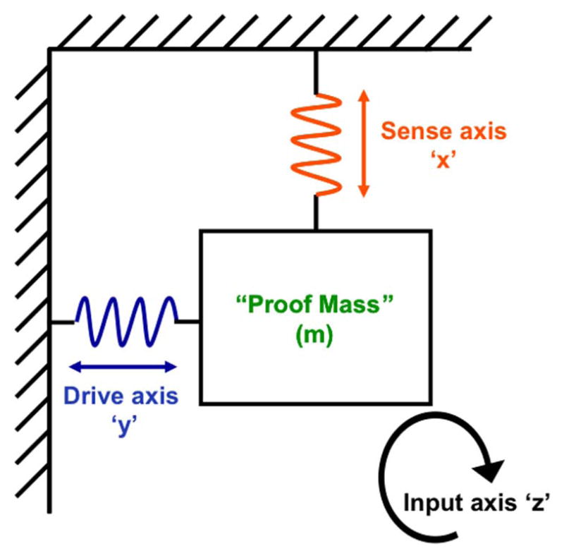
A MEMS gyroscope is driven in one axis and sensed in an orthogonal axis.
Fig. 28.

Gyroscope with electromagnetic excitation and piezoresistive detection. From Paoletti [278]. © 1996 IEEE.
Most micromachined gyroscopes are based on vibration. Vibratory gyroscopes use the transfer of energy between two vibration modes by the Coriolis force. Micromachined gyroscopes are difficult to manufacture, as they require a high performance resonator and an accelerometer, coupled in a high-vacuum hermetic package.
In most commercial MEMS gyroscopes, the same transduction scheme is preferred for both resonator actuation and acceleration sensing for ease of integration, e.g., piezoelectric or capacitive; this is one reason why piezoresistive gyroscopes are not seen in production. Another reason is the 1/f noise source. In most rate sensing applications, i.e., navigation, the primary variable of interest is position. However, a gyroscope senses rate of rotation and to obtain position the output of gyroscope must be integrated. As with any integration, the slightest offset errors will induce an increasing (ramped) error in the integrated position. Hence, the zero stability and 1/f noise of gyroscopes are of enormous importance for position sensing applications. Piezoresistor transduction has inherent 1/f noise that limits the useful integration time (accuracy) on the device output. Capacitive sensing gyroscopes are more commonly employed because they do not exhibit 1/f noise at the transducer. However, with progress in very low 1/f noise piezoresistors [56], piezoresistive gyroscopes may soon appear with new possibilities of improved quadrature signal cancellation.
3) Shear Stress Sensors
The accurate measurement of wall shear stress (or skin friction) is important for both applied and basic problems. From improving the aerodynamic design of a vehicle body to understanding the formation of atherosclerosis on the wall of human blood vessels [281], shear stress measurement provides key input to understanding the fluid flow physics. Naughton and Sheplak reviewed three relatively modern categories of skin-friction measurement techniques that are broadly classified as MEMS-based sensors, oil-film interferometry, and liquid crystal coatings [282]. While MEMS-based techniques show great promise, further development is needed and piezoresistive shear stress sensors are an area of active research [282], [283]. Piezoresistive shear stress sensors commonly utilize a floating-element anchored to the substrate via four piezoresistive tethers (fixed-guided beams). The displacement of the floating element due to the integrated shear stress (force) is detected as bending stress in the piezoresistors.
Ng et al. [284] and Shajii et al. [285] used wafer-bonding technology to fabricate floating-element (120 × 140 μm2) sensors. Piezoresistors were fabricated on the top surface of the tethers using ion implantation (Arsenic at 80 keV and 7 × 1015 cm−2 dose). In operation, the fluid flow direction was parallel to the tethers such that a shear force over the element loads two of the tethers in axial compressive stress and the other two in axial tensile stress. The sensor was designed to detect high shear stresses (1–100 kPa) in high pressure (6600 psi) and high temperature (220 °C) liquid environments, and was tested in a cone-plate viscometer.
We used oblique (20°) ion-implantation to form piezoresistors on the sidewall of two tethers and a normal surface implant for two other tethers (Fig. 29) [53]. The sidewall piezoresistors are sensitive to lateral deflections (Fz and My in the flow direction), while the normal piezoresistors are sensitive to flow fluctuations producing out-of-plane deflections (Fy and Mz). Thus, each sensor enabled simultaneous measurements of normal and shear stresses. The floating element (500 × 500 μm2) was defined using frontside and backside silicon DRIE processes. A hydrogen anneal (1000 °C and 10 mTorr for 5 minutes) smoothed the DRIE scallops before ion-implant and improved the 1/f noise level of the oblique-implanted piezoresistors by an order of magnitude. The sensors were designed for harsh, liquid environments, and were tested in a gravity-driven flume [150]. Li et al. also developed piezoresistive shear stress sensors using oblique ion-implantation technique, optimizing the geometry of the piezoresistors and the sensors, as well as the dopant concentration and bias voltage [125], [286]. Other piezoresistive 3D stress sensors have been used to measure multi-axis tactile or traction forces for biological [287]–[289], robotic [290], and device packaging applications [59]–[61], [69], [153], [291]–[294]. Noda et al. fabricated 2-D shear stress sensors for tactile sensing with standing piezoresistive cantilevers embedded in polydimethylsiloxane (PDMS) [295]. Fan et al. and Chen et al. have designed, fabricated, and characterized artificial-hair-cell-based piezoresistive flow sensors for underwater applications [296], [297]. These artificial haircells are inspired by biological hair-cells and utilized arrays of piezoresistive cantilevers with posts (hairs) normal to the cantilever. These sensors can also be used to measure shear stress with similar principles to those of piezoresistive fence-based shear stress sensors [298], [299].
Fig. 29.

(a) Piezoresistive floating-element MEMS shear stress sensor. Each sensor consists of two top-implanted and two sidewall-implanted piezoresistors. The sidewall-implanted piezoresistors are sensitive to in-plane stress (shear stress), while the top-implanted piezoresistors are sensitive to out-of-plane stress (normal stress). Thus, each sensor enables simultaneous measurements of normal and shear stresses. (b) SEM image of a 500-μm square floating element. (c) SEM image of one of the tethers with a sidewall-implanted piezoresistor. Reprinted from Barlian et al. [53] with permission from Elsevier.
E. Signal Conditioning and Temperature Compensation
As discussed in Sections II-D2 and II-E1, piezoresistors are also sensitive to temperature variations. In many cases, the resistance change due to temperature is higher than that of the desired signal. The electronics can correct for these changes. Moreover, processing variations also give rise to different piezoresistive characteristics, which in turn alter the temperature characteristics of each sensor. However, each piezoresistive sensor can be individually calibrated to achieve high accuracy. The most common temperature compensation techniques in piezoresistive sensors use identical resistors in a Wheatstone bridge configuration. Co-fabricated piezoresistors of the same design exhibit similar temperature dependence; therefore, the zero output of a compensated Wheatstone bridge remains constant with temperature changes (to first order). This scheme trades off favorably for signal-to-noise ratio (SNR) with increased sensitivity despite increased noise e.g., Mallon et al. [56]. Temperature-sensing resistors may also be co-fabricated with stress-sensing piezoresistors and used as bridge elements. These resistors should be placed near one another to minimize the effects of process variation. Modern electronics can ultimately correct all repeatable errors. If a piezoresistive sensor is heated and then cooled to the initial temperature, then the output should be the same for the same input. However, small differences are observed between temperature cycles. This thermal non-repeatability is one of the fundamental limits of sensor accuracy, not correctable with signal conditioning circuits.
Prior to 1980 most of the temperature compensation circuits for piezoresistive sensors employed trim resistors with or without low noise bipolar amplifiers. Laser-trimmed resistors are used to adjust the offset, span, nonlinearity and other errors of piezoresistive sensors. Laser-trimmed amplifiers are rather bulky due the mechanical limits placed on the trim resistors. CMOS circuitry became the dominant source of signal conditioning after 1990. The need for even smaller, more accurate, and cheaper sensors was an impetus for the transition to CMOS. The bipolar technology, an analog technology, does not offer the functionality of a digital technology (CMOS) measured in terms of cost per power per functionality. The push toward CMOS technology evolved with the availability of non-volatile memory (NVM). The laser-trimmed resistors were then replaced with digital-to-analog converters (DAC) and memory. By use of double correlated sampling, offset and low frequency noise of the CMOS circuit are sampled and stored on a capacitor and in the next cycle they are subtracted from the original signal. Hence rendering the CMOS amplifier almost ideal in the low frequency region relative to the sampling frequency. In CMOS, the need for digital output is easily addressed by integrating the analog to digital converter with the sensor. A majority of designs incorporate sigma-delta converters (Fig. 30) as the primary analog to digital converter (ADC) architecture due to its inherent robustness [300], [301].
Fig. 30.

(a) CMOS integrated piezoresistive cantilever array (two scanning cantilevers and one reference cantilever) (b) Micrograph of the overall sensor CMOS signal conditioning circuit (c) Array of 12 cantilevers (the inner ten can be used for scanning while the outer two serve as a reference). The dimensions of the scanning cantilevers are 500 μm × 85 μm. From Hafizovic et al. [305], reprinted with permission from PNAS.
By use of analog circuit techniques and NVM, the need for laser trimming as a means of sensor compensation was eliminated and the power of digital technology was used to compensate and calibrate the piezoresistive sensors. This technology enabled unprecedented sensor accuracy at very low cost [302].
There are two main architectures for piezoresistor temperature compensation, i.e., fully digital path and digitally controlled analog path [303]. Digital path architecture uses an ADC to digitize the sensor and temperature signal and then uses a mathematical equation to compensate offset and span. If an analog output is needed then the compensated digital data is fed to a DAC. This architecture is the most flexible but has some inherent problems that limit its use in control loops. One of the main drawbacks is the delay time from the input to output. The ADC, the microprocessor, and the DAC all need processing time, this dead time may not be tolerated in feedback control. In contrast, the analog path architecture takes advantage of the fact that temperature is a slow signal. Hence, delay in processing of the temperature signal is not of concern. The digitized temperature signal is mathematically processed and controls an analog path by changing the gain and the offset of wide-band amplifiers, which inherently have small delays.
The question of integration of the sensor with electronics mainly depends on the application. Generic signal conditioning circuitry consists of an excitation circuit, a bridge circuit, an amplifier, and a filter [51]. These components all contribute to the overall resolution of the system (Fig. 31). Ishihara et al. developed the first CMOS integrated silicon diaphragm pressure sensors in 1987 [304]. Since then, CMOS circuitry has been integrated with piezoresistive MEMS devices, such as AFM [63], [195], [205], [216], [219], [305]–[307] and force or stress sensors [59], [61], [68], [290], [292], [294], [308]–[310]. Mayer et al. determined three piezoresistive coefficients, π11, π12, and π44, of an n+ diffusion of a commercial piezoresistive CMOS chip using a novel method by subjecting the chip to three different stress fields [311]. This method can be used to calibrate CMOS-based piezoresistive stress sensor chips. Baltes et al. reviewed advances in the CMOS-based MEMS until 2002, including microsensors and packaging, and discussed some key challenges and applications for the future [312], [313]. Recently, more advanced techniques have been employed to achieve better control in temperature compensation. Chui et al. took advantage of the dependence of the piezoresistive coefficient of silicon on crystallographic orientation, and showed an order of magnitude improvement in thermal disturbance rejection over conventional approaches using uncoupled resistors by using piezoresistors in both the 〈100〉 and 〈110〉 directions [314].
Fig. 31.

The power spectral density (PSD) and integrated force noise of a measurement system using an AD622 instrumentation amplifier and piezoresistor bridge. All components in a signal conditioning circuit contribute to the noise and resolution of the system. Courtesy of Sung-Jin Park [54], reprinted with permission from PNAS.
Mallon et al. used a modulation-demodulation circuit to measure 1/f noise of piezoresistors at low frequencies [56]. The modulation demodulation technique is primarily used for low noise and low frequency detection of a sensor signal. This technique overcomes the high noise of electronics at low frequencies since all linear non-switched electronic amplifiers exhibit higher noise at low frequencies. The bridge is excited with sinusoidal voltage (10 Vpp). The output of the piezoresistive bridge is proportional to the applied voltage multiplied by conductivity variation. The modulated output of the piezoresistive bridge is then amplified (×1000) using a high frequency low noise amplifier (TI103), and then bandpass-filtered to reduce the effect of noise folding (bandwidth ~200 Hz, center frequency 500 Hz). Using a multiplier with gain of 4/π (AD630) the signal is demodulated. The signal is finally low-pass filtered with a three pole filter (Fig. 32).
Fig. 32.

Modulation-demodulation circuit for low frequency low noise detection.
F. Device Design Summary
Since the discovery of piezoresistance, several generations of commercial device designers and academic researchers have designed piezoresistive sensors for diverse applications. However, all piezoresistive sensors have fundamental tradeoffs between sensitivity and noise. The piezoresistor geometry, device geometry, and fabrication process must be designed together for low noise and high sensitivity to achieve the required resolution. Design constraints and flexibility have evolved with mainstream semiconductor technology providing new processes such as ion implantation and reactive ion etching. As discussed already, several investigators have provided detailed device optimization analyses for given applications within very specific constraints [46], [57], [149], [181]–[183], [213], [262]. No concise, generic design guidelines exist for all devices types and the sensitivity and noise are convolved with the geometry and mechanics of any particular device. However, the design criteria for the piezoresistor itself can be described by a rich parameter space and we review here many that are directly in control of the designer.
Design parameters include: dopant type, energy, and deposition method; the type, temperature and time of anneal(s); the thickness (tp), length (lp), and width (wp) of the piezoresistor and their relation to device geometry (e.g., ratio of piezoresistor length to beam length); and the number of dopant atoms (N) in the piezoresistor volume. The geometry and dimensions of the device are designed in parallel to meet bandwidth, dynamic range, sensitivity, and resolution requirements. Particular attention to the tradeoffs in parameters is required when pushing towards very small sizes, high sensitivity, or large bandwidth. Figs. 12, 15, and 18 and (13) and (14) provide quantitative guidance in the tradeoffs in selecting dopant concentration, anneal, and bias voltage to increase sensitivity and decrease noise. For example, the minimum force resolution in an ion implanted, end-loaded, piezoresistive cantilever in a 1/4-active Wheatstone bridge may be expressed as a function of (11), (12), (15), and (16) as
| (19) |
where γ is the ratio of the strained region of piezoresistance to the unstrained resistance path.
However the optimization must also be tempered with application specific requirements for device size, power dissipation, bandwidth, dynamic range, linearity, and temperature stability. For example, reduced power dissipation argues for higher overall resistance (lower N) and lower bias voltage. Lower carrier number (N) concomitantly increases the 1/f noise, resistance, sensitivity, temperature coefficients of sensitivity and resistance, while higher resistance increases Johnson noise. In determining dimensions for a displacement sensing cantilever, Table 3 provides a relational matrix between parameters the designer can tune to tailor device performance.
Table 3.
Example Design Matrix Showing Relationship of Parameters in Piezoresistive Cantilever Beam for Displacement Sensing [Trends Within the Ranges of Figs. 12, 15, 16 and 18 and (13) and (14)]. As the Controlled Design Parameter Increases (While Other Parameters Are Held at Typical Values and Input Displacement is Fixed), the Observed Parameters Respond as: Increasing (↑), Decreasing (↓), Weak or No Relation (-).
| Observed Parameters | |||||||||||
|---|---|---|---|---|---|---|---|---|---|---|---|
| Power (W) | Volume (m3) | Bandwidth & ωn (Hz) | Sheet resistance (Ω/square) | Sensitivity (V/m) | 1/f Noise (V/√Hz) | Johnson Noise (V/√Hz) | Junction depth (m) | TCR (/°C) | TCS (/°C) | ||
| Controlled Parameters | ↑ n (cm−3) | ↑ | - | - | ↓ | ↓ | ↓ | ↓ | - | * | ↓ |
| ↑ Vb (V) | ↑ | - | - | - | ↑ | ↑ | - | - | - | - | |
| ↑ Dt (m) | ↑ | ↑ | - | ↓ | ↓ | ↓ | ↓ | ↑ | - | - | |
| ↑ tp (m) | ↑ | ↑ | - | ↓ | ↓ | ↓ | ↓ | ↑ | - | - | |
| ↑ wp (m) | ↑ | ↑ | - | - | - | ↓ | ↓ | - | - | - | |
| ↑ lp (m) | ↓ | ↑ | - | - | ↓ | ↓ | ↑ | - | - | - | |
| ↑ h (m) | - | ↑ | ↑ | - | ↑ | - | - | - | - | - | |
| ↑ L (m) | - | ↑ | ↓ | - | ↓ | - | - | - | - | - | |
| ↑ b (m) | - | ↑ | - | - | - | - | - | - | - | - | |
Note: Please See Fig. 15.
Vb, Vb, and Dt are the Dopant Concentration, Bias Voltage, and Diffusion Length, Respectively. tp, wp, and lp are the Piezoresistor Thickness, Width, and Length, Respectively. h, b, and L are the Cantilever Beam Thickness, Width, and Length, Respectively
Generally, larger dimensions allow better sensitivity and larger piezoresistor size which lowers noise and improves heat dissipation. Beam dimensions are selected for dynamic range, sensitivity, and bandwidth. Minimum thickness is limited by process capability (Section III-C) and should also be selected to achieve appropriate piezoresistor strain and account for strains from residual stresses in dielectrics or thin films. Well-prepared, small-diameter samples of silicon exhibit high fracture stress [315], while processed MEMS devices of millimeter dimensions exhibit lower values [316].
Once devices are fabricated, testing usually involves characterization of noise power spectral density and sensitivity calibration of individual devices after packaging and integration with signal conditioning. The noise integrated over the measurement or application frequency band sets the resolution, reported by converting voltage output to the measurand using the sensitivity calibration. Calibration methods vary from device to device but should be accomplished over the temperature range, dynamic range, and bandwidth appropriate to the application. For example, piezoresistive cantilevers calibrated with an electrostatic force balance at the U.S. National Institute of Standards and Technology (NIST) are promising metrology devices as force transfer standards for MEMS and AFM users [317], [318].
IV. ALTERNATIVE PIEZORESISTIVE MATERIALS
Most commercial and research piezoresistive MEMS devices and microsystems utilize silicon and germanium, or their alloys. For example, Lenci et al. reported the first experimental values of piezoresistive coefficients in polycrystalline silicon-germanium and demonstrated a pressure sensor of this material [319]. They found longitudinal and transverse piezoresistive coefficients of 4.25 × 10⁻¹¹ Pa−1 and 0.125 × 10⁻¹¹ Pa−1, respectively. However, with advances in materials science and processing, newer materials are currently being developed for MEMS and microsystems. These materials have advantages over silicon in some applications (e.g., higher melting temperature, higher/lower modulus of elasticity, or higher piezoresistive coefficients). In this section, we review four novel materials that could complement silicon in piezoresistive sensing applications.
A. Silicon Carbide
Silicon Carbide (SiC), with superior mechanical properties, such as higher Young’s Modulus (424 GPa), higher sublime temperature (1800 °C), higher thermal conductivity, and inertness to corrosive environments, is an attractive new material for MEMS and NEMS devices [320]. In addition to its superior mechanical properties, single crystal SiC also has a wider band gap (2.39–3.33 eV) compared to that of single crystal silicon (1.12 eV) [320]. This reduces the effect of thermal generation of carriers that results in increased reverse leakage current across a p-n junction, at high temperatures. Werner and Fahrner summarized electronic maximum operating temperature and band gaps for several semiconductor materials [321]. SiC has several advantages over other wide-bandgap materials (GaAs, diamond, etc.), including commercial availability of substrates, some device processing techniques, and the ability to grow stable native oxides [320]. Nevertheless, obtaining a high-quality oxide with low interface state and oxide trap densities has proven challenging because of the carbon on the surface, as well as off-axis epitaxial layers which have rough surface morphologies [322].
SiC has about 200 known polytypes. The physical properties of each polytype vary. A complete review of SiC crystal structures and polytypes is available elsewhere [323]. The most common ones are 6H-SiC, 4H-SiC, and 3C-SiC. Polytypes 6H-SiC and 4H-SiC have a hexagonal crystal structure (α-SiC), while 3C-SiC has a cubic crystal structure (β-SiC). In one of the earliest systematic studies in the piezoresistivity of 3C-SiC, Shor et al. measured the longitudinal and transverse gauge factors as a function of temperature for two different doping levels [324]. Ziermann et al. reported the first piezoresistive pressure sensor using single crystalline β-SiC n-type piezoresistors on Silicon-on-Insulators (SOI) substrates [325]. Studies performed on the piezoresistivity of a-SiC have shown negative gauge factors as large as −35 for longitudinal and −20 for transverse gauge factors [326], [327]. A summary of published piezoresistive data for both α- and β-SiC through 2001 was presented by Werner et al. (Fig. 33) [328].
Fig. 33.

Longitudinal gauge factor in 〈100〉 direction for β-SiC as a function of temperature for different doping levels from various researchers [324], [325]. Werner et al. noted that these experimental data are in good agreement with the theoretical gauge factor predicted by electron transfer mechanism theory [81] in many-valley semiconductors [328]. After Werner et al. [328]. Reprinted with permission from Wiley.
In contrast to its single crystal counterpart, polycrystalline SiC exhibits positive gauge factors of smaller magnitude. Strass et al. provided a summary of the gauge factor of polycrystalline SiC as a function of temperature and doping [329]. At room temperature, the gauge factor is around 6 for undoped and 2–5 for doped polycrystalline SiC. The shift from negative to positive values was explained by the greater influence of grain boundaries in polycrystalline wide-bandgap materials compared to polysilicon. The piezoresistance also depends on the temperature, the crystal orientation, and the doping type.
Piezoresistance of polycrystalline β-SiC fibers has also been studied [330]. With a gauge factor of 5 in 14-μm diameter β-SiC fibers under tension, SiC fibers have been used for continuous reinforcement of high-temperature structural composites for their oxidation resistance. Their piezoresistive properties are useful to monitor strain in these composites.
Additionally, theoretical investigations of the piezoresistivity in the cubic 3C-SiC and hexagonal n-type 6H-SiC, based on electron transfer and the mobility shift mechanism, have been performed [331], [332]. In the hexagonal 6H-SiC, the anisotropic part of the piezoresistance tensor vanishes in the (0001) plane and only the isotropic part remains. As a consequence, longitudinal, transverse, and shear gauge factors and properties are isotropic in the (0001) plane.
Several SiC-based piezoresistive MEMS devices have been developed to withstand harsh operating environments, such as high impact/acceleration (40 000g) [333] and high temperatures (200–500 °C) [334]–[336]. Complete reviews of SiC-based MEMS and NEMS, especially for harsh environment applications, are available elsewhere [321], [328], [337]–[340].
B. Diamond
Diamond is also an attractive new material for micromechanical devices for elevated temperatures and harsh environments [321], [328], [341], [342]. Superior properties, compared to silicon, include physical hardness, higher Young’s modulus, higher tensile yield strength, greater chemical inertness, lower coefficient of friction, and higher thermal conductivity. Experimental values for Young’s modulus of CVD diamond have been reported from 980 to 1161 GPa [341].
Doping of diamond can be done in-situ during film growth, or using other standard techniques, such as ion implantation and high-temperature diffusion. Werner et al. summarized both longitudinal and transverse piezoresistive coefficients reported by various research groups before 1998 (Fig. 34) [342]. The reported piezoresistive GF of single crystal and polycrystalline diamond are typically in the ranges of 2000–3836 and 10–100, respectively [343]. Polycrystalline diamond has a higher GF compared to that of SiC, but like the other piezoresistive properties, these values depend greatly on the doping concentration and temperature.
Fig. 34.

The summary of published average longitudinal and transverse piezoresistance coefficients in boron-doped polycrystalline diamond by Werner et al. [342]. The published gauge factor data were converted to piezoresistive coefficients assuming Young’s modulus of 1143 × 109 Pa. After Werner et al. [342]. © 1998 IEEE.
The relatively low GF of polycrystalline diamond is usually attributed to its polycrystalline structure. A study of intra- and inter-grain conduction in large-grain CVD diamond showed the intra-grain resistivities are lower than those of grain boundaries [343]. The intra-grain GF over 4000 for a large grain (50–80 μm) polycrystalline diamond is the largest piezoresistive effect reported for any material. However, the GF deteriorates when grain boundaries are included in the conductance path, with a GF of 133 when the conductance path includes eight grain-boundaries. Yamamoto and Tsutsumoto suggested two methods to improve the GF of polycrystalline diamond films [344]. The first was to decrease the ratio of carbon to hydrogen when depositing boron-doped diamond films. Decreasing the ratio of C-O/H from 5.5% to 2.2%, increased the GF from 3 to 30. In this case, the quality of diamond was improved by decreasing the C-O/H ratio and the GF increased as the diamond quality was improved and the grain size became larger. A second method varied boron doping time and the boron-doped layer thickness. Varying doping time from 3 to 10 minutes (corresponding to layer thickness of 0.1 to 0.33 μm) increased the GF from 0 to 50.
C. Carbon Nanotubes (CNT)
Carbon nanotubes (CNTs) are graphene sheets rolled-up into cylinders with diameters as small as one nanometer and lengths as large as centimeters. This form of carbon was first reported by Iijima in 1991 [345]. Mechanically, nanotubes are among the strongest and most resilient materials known in nature. CNT Young’s modulus is on the order of TPa with tensile strength two orders of magnitude higher than that of steel [346]. Electronically, CNTs can be metallic, semiconducting, or small-gap semiconducting (SGS) [347]. Qian et al. reviewed theoretical predictions and experimental techniques that are widely used for visualization, manipulation, and measurements of mechanical properties of CNTs [348]. Most experiments use an AFM tip to deflect a CNT suspended over a trench and several experiments have measured electromechanical properties of CNTs [349]–[351]. The piezoresistance is attributed to energy band shifts and is observed as a shift in nonlinear CNT I-V curves. Fung et al. integrated bundled strands of CNT on polymer-based diaphragms of microfabricated pressure sensors using dielectrophoretic (DEP) nanoassembly [352]. Grow et al. reported measurements of the electromechanical response of CNTs adhered to pressurized membranes [353]. Single-tube CNTs adhered to silicon nitride membranes by van der Waals interactions, were electrically connected in-situ and assumed to experience the same strain as the membrane (Fig. 35). The conductivity of the CNT decreased as the membrane was pressurized (0 ~ 15 psi). This CNT pressure sensor had a resolution of 1 psi with CNT gauge factors of 400 and 850 for semiconducting and SGS tubes, respectively. Possible applications include integration of nanotubes on or in a variety of substrates, including flexible plastics. Chiamori et al. [354] incorporated single-wall nanotubes (SWNT) into the negative resist material, SU-8, and investigated the SU-8/SWNT nano-composite electromechanical properties, such as effective Young’s modulus and piezoresistivity. We found a gauge factor of 2–4 for the 1–5 wt% (weight percent) SU-8/SWNT composite and an effective Young’s modulus of about 0.5 GPa for the 1 wt% composite. Complete reviews of electromechanical properties and other applications of CNT are available elsewhere [347], [355], [356].
Fig. 35.

(a) Schematic of a CNT device on a membrane (b) Optical microscope image of a membrane with electrodes (c) Zoomed in image of devices near the edge of a membrane (d) SEM Image of a CNT crossing the gap between two electrodes (~800 nm). Reprinted with permission from Grow [353]. © 2005 American Institute of Physics.
D. Nanowires
Nanowires, also known as quantum wires, are electrically conducting wires, in which quantum transport effects are important. As the width of the wire is reduced to Fermi wavelength scale, the conductance between the electrodes connected by the nanowire is quantized in steps of 2e2/h (where e is the charge of the electron and h is the Planck’s constant) and conductance is no longer dependent on the length of the wire [357]. Different types of nanowires, e.g., metallic, semiconducting, insulating, and molecular (organic and inorganic) have different electromechanical properties. Nanoindentation is a popular method to determine the hardness and elastic modulus of nanowires, such as gallium nitride (GaN) and zinc oxide (ZnO) nanowires, tantalum oxide (Ta2O5) nanowires, single-crystal and polycrystalline copper nanowires, and gold nanowires [357]–[362]. Zhu and Espinosa, Desai et al., and Lu et al. have also developed MEMS experimental test beds for electromechanical testing of nanowires [359], [362], [363].
To date, relatively few reports on the development of silicon nanowire-based sensors are available [364]. However, p-type single crystalline silicon nanowires have been studied for sensor applications [365], [366]. Separation by implanted oxygen (SIMOX), thermal diffusion, electron beam (EB) direct writing, and reactive ion etching (RIE) have been used to fabricate silicon nanowire piezoresistors [365]. Both the longitudinal and transverse piezoresistive coefficients, πl[011] and πt[011], are dependant on the cross sectional area of the nanowires. The πl[011] of the nanowire piezoresistors increased (up to 60%) with a decrease in the cross sectional area, while πt[011] decreased with a decrease in the cross sectional area (Fig. 36). The enhancement behavior of the πl[011] was explained qualitatively using 1-D hole transfer and hole conduction mass shift mechanisms. The decrease in the πt[011] with decrease in the cross sectional area is due to decrease in the stress transmission from substrate to the nanowire. The maximum value, πl[011] of 48 × 10−11 Pa−1 at a surface concentration of 5 × 1019 cm−3, suggests enough sensitivity for sensing applications. Dao et al. incorporated these p-type silicon nanowires as piezoresistive elements in a miniaturized 3-degrees-of-freedom (3-DOF) accelerometer [367]. Roukes and Tang patented strain sensors based on cantilever-embedded nanowire-piezoresistor wires and ultra-high density free-standing nanowire arrays [368].
Fig. 36.

Size (cross sectional area) effect on longitudinal and transverse piezoresistive coefficients in boron-doped nanowires fabricated using electron beam (EB) lithography and reactive-ion-etching (RIE). After Toriyama [366]. © 2002 IEEE.
He and Yang reported on very large piezoresistance effect (commonly referred to as “giant piezoresistance”) in p-type silicon nanowires, particularly in the 〈111〉 direction [369]. The measured piezoresistance values were a function of the nanowires diameters and resistivities, with the largest value of −3550 × 10−11 Pa−1 in the longitudinal direction. Silicon nanowires in the 〈111〉 direction, with diameters of 50–350 nm and resistivities of 0.003–10 Ω cm, were grown and anchored to a silicon substrate (from SOI wafers) to form a bridge structure (Fig. 37) and uniaxial stress was applied to the nanowires using a four-point bending setup. Cao et al. explained the giant piezoresistance phenomenon in 〈111〉 silicon nanowires based on a first-principles density-functional analysis and identified “the strain-induced band switch between two surface states, caused by unusual relaxation behavior in the surface region,” as the key contributor [370]. Their model and calculations captured all the main features of the experimental results by He and Yang. Following the experimental results from He and Yang, Reck et al. used a lift-off and an electron beam lithography (EBL) technique to fabricate silicon test chips and study the piezoresistive properties of crystalline and polycrystalline nanowires as a function of stress and temperature [371]. Compared to the bulk silicon’s piezoresistive effect, they found a 633% and 34% increase in piezoresistive effect for the crystalline and polysilicon nanowires, respectively. They also found that the piezoresistive effect greatly increases as the nanowire diameter decreases, consistent with the results from He and Yang [369].
Fig. 37.

(a) A 〈111〉 nanowire grown and anchored onto a silicon substrate. (b) morphology of a bridged nanowire along the 〈111〉 direction. (c) Transmission Electron Microscopy (TEM) images of the left joint between the sidewall and the nanowire bridge. (d) Longitudinal piezoresistive coefficients of 〈111〉 nanowires as a function of the nanowire diameter and resistivity. Piezoresistive coefficients from bulk silicon are also included. The scale bars in (a)–(c) are 2 μm, 500 nm, and 100 nm, respectively. From He and Yang [369]. Reprinted with permission from Macmillan Publishers Ltd.: Nature Nanotechnology [369] © 2006.
V. CONCLUSION
With the discovery of the large piezoresistive coefficients in silicon in 1954, the study of piezoresistance moved from scientific inquiry of a material property to extensive investigation, development and commercialization. Piezoresistor development largely followed that of the mainstream semiconductor industry. Integration of piezoresistors with micromachined flexure elements enabled widespread implementation of these MEMS sensors. Piezoresistance has become a fundamental sensing modality in the toolbox of MEMS sensor designers. Recent research focuses on driving to the nanoscale, using high band gap semiconductors to make high pressure, high temperature sensors, and applying piezoresistive cantilevers to biological and chemical sensing. Building on over fifty years of research, the field remains active and vibrant.
Acknowledgments
Research in the Pruitt Microsystems Laboratory related to piezoresistance has been supported by the National Science Foundation under awards ECCS-0708031, ECS-0449400, CTS-0428889, ECS-0425914, and PHY-0425897 and the National Institutes of Health under award R01 EB006745-01A1.
The authors are grateful to Dr. M. A. Hopcroft, Dr. M. Doelle, P. Ponce, N. Harjee, S.-J. Park, and P. Lim for helpful discussions.
Biographies

A. Alvin Barlian received the B.S. degree with Honors and Distinction from Purdue University, West Lafayette, IN, in 2001 and the M.S. and Ph.D. degrees from Stanford University, Stanford, CA, in 2003 and 2009, respectively, all in mechanical engineering.
His doctoral research focused on the development of micro-fabricated piezoresistive shear stress sensors for harsh liquid environments, characterization of microfabricated piezoresistive cantilevers for force sensing applications, and a novel sidewall epitaxial piezoresistor fabrication process for in-plane force sensing applications (U.S. patent, pending). In 2008, he worked on the characterization of capacitive RF MEMS switches as an Interim Engineering Intern with the Technology R&D Department at Qualcomm MEMS Technologies.
In 2007, he was presented the Centennial Teaching Assistant Award by Stanford University for his efforts in co-developing a micro/nanofabrication laboratory course at Stanford University. In 2005, he received the Best Poster Award for the most outstanding poster presentation at the International Mechanical Engineering Congress and Exposition in Orlando, FL. In 2001, he was inducted into the Honor Society of Phi Kappa Phi and he received the John M. Bruce Memorial Scholarship from Purdue University. He was the P.T. Caltex Pacific Indonesia scholar from 1998 to 2002.

Woo-Tae Park received the B.S. degree in mechanical design from Sungkyunkwan University, Seoul, Korea, in 2000, the M.S. and Ph.D. degrees in mechanical engineering from Stanford University, Stanford, CA, in 2002 and 2006 respectively.
For his graduate degree work, he worked on optical measurements for electrical contact deformation, wafer scale encapsulated MEMS devices, and submillimeter piezoresistive accelerometers for biomedical applications. After graduation, he started as a senior packaging engineer at Intel, designing silicon test chips for assembly, test, and reliability. He is now with Freescale semiconductor, working on MEMS process development in the Sensor and Actuator Solutions Division. Dr. Park has authored seven journal papers, fifteen conference papers and holds one patent.

Joseph R. Mallon, Jr. received the B.S. degree in science (cum laude) from the Fairleigh Dickinson University and the MBA degree in Management, Marketing and New Venture from California State University, Hayward, CA. From 1965 to 1985, Mr. Mallon was the Vice President of Engineering for Kulite Semiconductor Products, one of the earliest MEMS sensor companies. From 1985 to 1993, he was the Co-President, COO, Co-Founder, and Director of NovaSensor, a venture funded Silicon Valley firm that helped establish MEMS as a widely known and commercial technology. Mr. Mallon was the Chairman and CEO of Measurement Specialties, a publicly traded sensor manufacturer, from 1995 until 2002. Currently he is studying and doing research at Stanford University along with his position as the CEO of axept. Mr. Mallon is a pioneer in MEMS technology with forty-five patents and over sixty technical papers and presentations.

Ali J. Rastegar received the B.S. and M.S. degrees in electrical engineering from the Worcester Polytechnic Institute in 1982 and 1984, respectively. He then joined Analog Devices as an integrated circuit design engineer where he developed several high-speed, state of the art analog-to-digital converters. In 1992, he founded MCA-technologies which was purchased by Maxim integrated products in 1997. In 2001 Mr. Rastegar became fascinated with the information storage capabilities of living cells and decided to further his understanding by pursuing the Ph.D. degree and joining the Stanford Microsystems Laboratory. Mr. Rastegar has designed more than 54 integrated circuits and holds eight issued U.S. patents.

Beth L. Pruitt (B.S. MIT 1991, M.S. 1992 and Ph.D. 2002 Stanford University) developed Piezoresistive Cantilevers For Characterizing Thin-Film Gold Electrical Contacts during her Ph.D. In 2002 she worked on nanostencils and polymer MEMS in the Laboratory for Microsystems and Nanoengineering at the Swiss Federal Institute of Technology (EPFL). She joined the Mechanical Engineering faculty of Stanford in Fall 2003 and started the Stanford Microsystems Lab. Her research includes piezoresistance, MEMS and Manufacturing, micromechanical characterization techniques, biomechanics of mechanotransduction, the development of processes, sensors and actuators as well as the analysis, design, and control of integrated electro-mechanical systems. Her research includes instrumenting and interfacing devices between the micro and macro scale, understanding the scaling properties of physical and material processes and finding ways to reproduce and propagate new technologies efficiently and repeatably at the macro-scale.
Prior to her Ph.D. at Stanford, Beth Pruitt was an officer in the U.S. Navy, at the engineering headquarters for nuclear programs and as a Systems Engineering instructor at the U.S. Naval Academy, where she also taught offshore sailing.
Footnotes
This paper provides a comprehensive overview of integrated piezoresistor technology with an introduction to the physics of piezoresistivity, process and material selection and design guidance useful to researchers and device engineers.
Contributor Information
A. Alvin Barlian, Email: barlian@stanfordalumni.org.
Woo-Tae Park, Email: wtpark@mems.stanford.edu.
Joseph R. Mallon, Jr, Email: mallon@stanford.edu.
Ali J. Rastegar, Email: alir1@stanford.edu.
Beth L. Pruitt, Email: pruitt@stanford.edu.
References
- 1.Bryzek J. MEMS: A closer look at part 2: The MEMS industry in Silicon Valley and its impact on sensor technology. Sensors. 1996 Jul 4; [Google Scholar]
- 2.Knutti JW. Micromachining and Microfabrication Process Technology IV. Santa Clara, CA: 1998. Finding markets for microstructures; pp. 17–23. [Google Scholar]
- 3.Thomson W. On the electro-dynamic qualities of metals: Effects of magnetization on the electric conductivity of nickel and of iron. Proc R Soc London. 1856;8:546–550. [Google Scholar]
- 4.Tomlinson H. On the increase in resistance to the passage of an electric current produced on wires by stretching. Proc R Soc London. 1876;25:451–453. [Google Scholar]
- 5.Tomlinson H. The influence of stress and strain on the action of physical forces. Philos Trans R Soc London. 1883;174:1–172. [Google Scholar]
- 6.Bridgman PW. Some properties of single metal crystals. Proc Nat Acad Sci USA. 1924;10:411–415. doi: 10.1073/pnas.10.10.411. [DOI] [PMC free article] [PubMed] [Google Scholar]
- 7.Bridgman PW. General survey of the effects of pressure on the properties of matter. Proc Phys Soc. 1928;41:341. [Google Scholar]
- 8.Bridgman PW. The effect of homogeneous mechanical stress on the electrical resistance of crystals. Phys Rev. 1932;42:858. [Google Scholar]
- 9.Williams WE. Phil Mag. 1907;13 [Google Scholar]
- 10.Rolnick H. Tension coefficient of resistance of metals. Phys Rev. 1930;36:506–512. [Google Scholar]
- 11.Allen M. The effect of tension on the electrical resistance of single bismuth crystals. Phys Rev. 1932;42:848–858. [Google Scholar]
- 12.Allen M. The effect of tension on the electrical resistance of single antimony crystals. Phys Rev. 1933;43:569–576. [Google Scholar]
- 13.Allen M. The tension coefficients of resistance of the hexagonal crystals zinc and cadmium. Phys Rev. 1936;49:248–253. [Google Scholar]
- 14.Allen M. The effect of tension on the electrical resistance of single tetragonal tin crystals. Phys Rev. 1937;52:1246–1249. [Google Scholar]
- 15.Cookson JW. Theory of the piezo-resistive effect. Phys Rev. 1935;47:194–195. [Google Scholar]
- 16.Pockels F. Elektrizitat und Magnetismus I (Handbuch der Physik vol. 4) 1905 [Google Scholar]
- 17.Trainer M. Kelvin and piezoelectricity. Eur J Phys. 2003;24:535–542. [Google Scholar]
- 18.Curie J, Curie P. Developpement, par pression, de l’electricite polaire dans les cristaux hemiedres a faces inclinees. C R Acad Sci. 1880;91:294–295. [Google Scholar]
- 19.Voigt W. Lehrbuch der Kristallphysik. Leipzig: 1910. [Google Scholar]
- 20.Thomson W. Elements of a mathematical theory of elasticity. Philos Trans R Soc London. 1856;146:481–498. [Google Scholar]
- 21.Thomson W. Note by Lord Kelvin on electric molecules for the explanation of the piezoelectric and pyro-electric properties of crystals. Phil Mag. 1893;36:1. [Google Scholar]
- 22.Thomson W. On the theory of pyro-electricity and piezo-electricity of cyrstals. Phil Mag. 1893;36:453–459. [Google Scholar]
- 23.Thomson W. On the piezo-electric property of quartz. Phil Mag. 1893;36:331–342. [Google Scholar]
- 24.Clark D, Datwyler G. American Society for Testing and Materials. 1938;39:98. [Google Scholar]
- 25.Stein PK. 1936—A banner year for strain gages and experimental stress analysis—An historical perspective. Experimental Techniques. 2006 Jan.30:23–41. [Google Scholar]
- 26.Simmons EE. 2 344 647. Method and apparatus for making strain gauges. 1944 Mar 21;
- 27.Simmons EE. Strain gauge. 2 393 714. US Patent. 1946 Jan;
- 28.Ruge AC. 2 350 972. Strain gage. 1944 Jun 6;
- 29.Bardeen J, Shockley W. Deformation potentials and mobilities in non-polar crystals. Phys Rev. 1950;80:72–80. [Google Scholar]
- 30.Smith CS. Piezoresistance effect in germanium and silicon. Phys Rev. 1954;94:42–49. [Google Scholar]
- 31.Mason WP, Thurston RN. Use of piezoresistive materials in the measurement of displacement, force, and torque. J Acous Soc of Am. 1957;29:1096–1101. [Google Scholar]
- 32.Sanchez JC, Wright WV. Recent developments in flexible silicon strain gages. In: Dean M, editor. Semiconductor and Conventional Strain Gages. New York: Academic Press; 1962. pp. 307–345. [Google Scholar]
- 33.Nielsen HA. From Locomotives to Strain Gages. New York: Vantage Press; 1985. [Google Scholar]
- 34.Hoerni JA. Planar silicon diodes and transistors. Electron Devices Meeting, 1960 International; 1960. p. 50. [Google Scholar]
- 35.Pfann WG, Thurston RN. Semiconducting stress transducers utilizing the transverse and shear piezoresistance effects. J Appl Phys. 1961;32:2008–2019. [Google Scholar]
- 36.Tufte ON, Chapman PW, Long D. Silicon diffused-element piezoresistive diaphragms. J Appl Phys. 1962;33:3322–3327. [Google Scholar]
- 37.Petersen KE. Silicon as a mechanical material. Proc IEEE. 1982;70:420–457. [Google Scholar]
- 38.Paul O, Gaspar J, Ruther P. Advanced silicon microstructures, sensors, and systems. IEEJ Trans. 2007;2:199–215. [Google Scholar]
- 39.Wise KD. Integrated sensors, MEMS, and microsystems: Reflections on a fantastic voyage. Sens Actuators, A. 2007;136:39–50. [Google Scholar]
- 40.Brantley WA. Calculated elastic constants for stress problems associated with semiconductor devices. J App Phys. 1973 Jan.44:534–535. [Google Scholar]
- 41.Franca DR, Blouin A. All-optical measurement of in-plane and out-of-plane Young’s modulus and Poisson’s ratio in silicon wafers by means of vibration modes. Meas Sci Technol. 2004;15:859–868. [Google Scholar]
- 42.Sokolnikoff IS. Mathematical Theory of Elasticity. Malabar, FL: R.E. Krieger Pub. Co; 1983. [Google Scholar]
- 43.Nathan A, Baltes H. Microtransducer CAD: Physical and Computational Aspects. Wien, NY: Springer-Verlag; 1999. [Google Scholar]
- 44.Kittel C. Introduction to Solid State Physics. 8. New York: John Wiley & Sons; 2005. [Google Scholar]
- 45.Nye JF. Physical Properties of Crystals: Their Representation by Tensors and Matrices. Oxford University Press; 1985. [Google Scholar]
- 46.Kanda Y, Yasukawa A. Optimum design considerations for silicon piezoresistive pressure sensors. Sens Actuators, A. 1997;62:539–542. [Google Scholar]
- 47.Kanda Y. A graphical representation of the piezoresistance coefficients in silicon. IEEE Trans Electron Devices. 1982;29:64–70. [Google Scholar]
- 48.Richter J, Hansen O, Larsen AN, Hansen JL, Eriksen GF, Thomsen EV. Piezoresistance of silicon and strained Si0.9Ge0.1. Sens Actuators, A. 2005;123–124:388–396. [Google Scholar]
- 49.Young WC, Budynas R. Roark’s Formulas for Stress and Strain. 7. New York: McGraw-Hill; 2002. [Google Scholar]
- 50.Wortman JJ, Evans RA. Young’s modulus, shear modulus, and Poisson’s ratio in silicon and germanium. J Appl Phys. 1965;36:153–156. [Google Scholar]
- 51.Senturia SD. Microsystem Design. New York: Springer; 2004. [Google Scholar]
- 52.Davenport AA, Lim P, Pruitt BL. Noise studies in implanted piezoresistors. ASME International Mechanical Engineering Congress and Exposition; Orlando, FL. 2005. [Google Scholar]
- 53.Barlian AA, Park SJ, Mukundan V, Pruitt BL. Design and characterization of microfabricated piezoresistive floating element-based shear stress sensors. Sens Actuators, A. 2007;134:77–87. [Google Scholar]
- 54.Park SJ, Goodman MB, Pruitt BL. Analysis of nematode mechanics by piezoresistive displacement clamp. Proc Nat Acad Sci USA. 2007 Oct. 30104:17376–17381. doi: 10.1073/pnas.0702138104. [DOI] [PMC free article] [PubMed] [Google Scholar]
- 55.Barlian AA, Harjee N, Mukundan V, Fung TH, Park S-J, Pruitt BL. Sidewall epitaxial piezoresistor process for in-plane sensing applications. 21st IEEE International Conference on Micro Electro Mechanical Systems; Tucson, AZ. 2008. pp. 331–334. [Google Scholar]
- 56.Mallon JR, Rastegar AJ, Barlian AA, Meyer MT, Fung TH, Pruitt BL. Low 1/f noise, full bridge, microcantilever with longitudinal and transverse piezoresistors. App Phys Lett. 2008;92:033508-1–033508-3. [Google Scholar]
- 57.Park S-J, Rastegar AJ, Fung TH, Barlian AA, Mallon JR, Pruitt BL. Optimization of piezoresistive cantilever performance. Digest Tech. Solid-State Sensors and Actuators Workshop; Hilton Head Island, SC. 2008. pp. 98–101. [Google Scholar]
- 58.Gragg JJE. Silicon pressure sensor. 4 317 126. US Patent. 1982 Feb 23;
- 59.Gieschke P, Richter J, Joos J, Ruther P, Paul O. Four-degree-of-freedom solid state MEMS joystick. MEMS 2008. IEEE 21st International Conference on Micro Electro Mechanical Systems; 2008. pp. 86–89. [Google Scholar]
- 60.Doelle M, Mager D, Ruther P, Paul O. Geometry optimization for planar piezoresistive stress sensors based on the pseudo-Hall effect. Sens Actuators, A. 2006;127:261–269. [Google Scholar]
- 61.Doelle M, Peters C, Ruther P, Paul O. Piezo-FET stress-sensor arrays for wire-bonding characterization. J Microelectromech Syst. 2006;15:120–130. [Google Scholar]
- 62.Creemer JF, Fruett F, Meijer GCM, French PJ. The piezojunction effect in silicon sensors and circuits and its relation to piezoresistance. IEEE Sensors J. 2001;1:98–108. [Google Scholar]
- 63.Akiyama T, Staufer U, de Rooij NF, Lange D, Hagleitner C, Brand O, Baltes H, Tonin A, Hidber HR. Integrated atomic force microscopy array probe with metal-oxide-semiconductor field effect transistor stress sensor, thermal bimorph actuator, and on-chip complementary metal-oxide-semiconductor electronics. J Vac Sci Technol, B. 2000;18:2669–2675. [Google Scholar]
- 64.Ivanov T, Gotszalk T, Sulzbach T, Chakarov I, Rangelow IW. AFM cantilever with ultra-thin transistor-channel piezoresistor: Quantum confinement. Microelectron Eng. 2003;67–68:534–541. [Google Scholar]
- 65.Shekhawat G, Tark SH, Dravid VP. MOSFET-embedded microcantilevers for measuring deflection in biomolecular sensors. Science. 2006;311:1592–1595. doi: 10.1126/science.1122588. [DOI] [PubMed] [Google Scholar]
- 66.Puers B, Reynaert L, Snoeys W, Sansen W. A new uniaxial accelerometer in silicon based on the piezojunction effect. IEEE Trans Electron Devices. 1988;35:764–770. [Google Scholar]
- 67.Fruett F, Meijer GCM. A test structure to characterize the piezojunction effect and its influence on silicon temperature sensors. Eurosensors XIII; The Hague, The Netherlands. 1999. pp. 53–56. [Google Scholar]
- 68.Fruett F, Meijer GCM. The influence of the piezojunction effect at different temperatures on the accuracy of silicon temperature sensors. ICMP/2000; Manaus, Brazil. 2000. [Google Scholar]
- 69.Jaeger RC, Suhling JC, Ramani R, Bradley AT, Xu J. CMOS stress sensors on (100) silicon. IEEE J Solid-State Circuits. 2000;35:85–95. [Google Scholar]
- 70.Meijer GCM. PhD. Delft Univ. Technol; 1982. Integrated circuits and components for bandgap references and temperature Transducers. [Google Scholar]
- 71.Pierret RF. Semiconductor Fundamentals: Modular Series on Solid State Devices. Addison-Wesley; 1983. [Google Scholar]
- 72.Pierret RF. Semiconductor Device Fundamentals. 2. Reading, MA: Addison Wesley; 1996. [Google Scholar]
- 73.Sun Y, Thompson SE, Nishida T. Physics of strain effects in semiconductors and metal-oxide-semiconductor field-effect transistors. J App Phys. 2007;101:104503 1–104503 22. [Google Scholar]
- 74.Kimball GE. The electronic structure of diamond. J Chem Phys. 1935;3:560–564. [Google Scholar]
- 75.Mullaney JF. Optical properties and electronic structure of solid silicon. Phys Rev. 1944;66:326–339. [Google Scholar]
- 76.Herring C. Transport properties of a many valley semiconductor. Bell Syst Tech J. 1955 Mar.34:237–290. [Google Scholar]
- 77.Herring C. Transport and deformation-potential theory for many-valley semiconductors with anisotropic scattering. Phys Rev. 1956;101:944. [Google Scholar]
- 78.Long D. Stress dependence of the piezoresistance effect. J App Phys. 1961;32:2050–2051. [Google Scholar]
- 79.Tufte ON, Stelzer EL. Piezoresistive properties of silicon diffused layers. J App Phys. 1963;34:313–318. [Google Scholar]
- 80.Herring C. Theory of the thermoelectric power of semiconductors. Phys Rev. 1954;96:1163–1187. [Google Scholar]
- 81.Keyes RW. The Effects of Elastic Deformation on the Electrical Conductivity of Semiconductors. Vol. 11. New York: Academic Press; 1960. [Google Scholar]
- 82.Becker M, Fan HY. Optical properties of semiconductors. III. infra-red transmission of silicon. Phys Rev. 1949;76:1531–1532. [Google Scholar]
- 83.Fan HY. Temperature dependence of the energy gap in monatomic semiconductors. Phys Rev. 1950;78:808–809. [Google Scholar]
- 84.Abeles B. Theory of the galvanomagnetic effects in germanium. Phys Rev. 1954;95:31–37. [Google Scholar]
- 85.Shibuya M. Magnetoresistance effect in cubic semiconductors with spheroidal energy surfaces. Phys Rev. 1954;95:1385–1393. [Google Scholar]
- 86.Meiboom S. Theory of the galvanomagnetic effects in n-germanium. Phys Rev. 1954;93:1121–1121. [Google Scholar]
- 87.Keyes RW. Explaining strain: The positive and negative effects of elastic strain in n-silicon. IEEE Circuits Devices Mag. 2002;18:36–39. [Google Scholar]
- 88.Lin MS. A better understanding of the channel mobility of Si MOSFETs based on the physics of quantized subbands. IEEE Trans Electron Devices. 1988;35:2406–2411. [Google Scholar]
- 89.Matsuda K. Strain-dependent hole masses and piezoresistive properties of silicon. IWCE-10 10th International Workshop on Computational Electronics; 2004. pp. 173–174. [Google Scholar]
- 90.Ohmura Y. Role of the valence band density of states in the piezoresistance of p-type semiconductors Si and Ge. J Phys Soc Jpn. 1993 Oct.62:3615–3620. [Google Scholar]
- 91.Fischetti MV, Ren Z, Solomon PM, Yang M, Rim K. Six-band k-p calculation of the hole mobility in silicon inversion layers: Dependence on surface orientation, strain, and silicon thickness. J App Phys. 2003;94:1079–1095. [Google Scholar]
- 92.Oberhuber R, Zandler G, Vogl P. Subband structure and mobility of two-dimensional holes in strained Si/SiGe MOSFET’s. Phys Rev B. 1998;58:9941–9948. [Google Scholar]
- 93.Toriyama T, Sugiyama S. Analysis of piezoresistance in p-type silicon for mechanical sensors. J Microelectromech Syst. 2002;11:598–604. [Google Scholar]
- 94.Bir GL, Pikus GE. Symmetry and Strain-Induced Effects in Semiconductors. New York: John Wiley & Sons; 1974. [Google Scholar]
- 95.Kleiner WH, Roth LM. Deformation potential in germanium from optical absorption lines for exciton formation. Phys Rev Lett. 1959;2:334–336. [Google Scholar]
- 96.Pikus GE, Bir GL. Cyclotron and paramagnetic resonance in strained crystals. Phys Rev Lett. 1961;6:103–105. [Google Scholar]
- 97.Hensel JC, Feher G. Valence band parameters in silicon from cyclotron resonances in crystals subjected to uniaxial stress. Phys Rev Lett. 1960;5:307–310. [Google Scholar]
- 98.Hasegawa H. Theory of cyclotron resonance in strained silicon crystals. Phys Rev. 1963;129:1029–1040. [Google Scholar]
- 99.Hensel JC, Feher G. Cyclotron resonance experiments in uniaxially stressed silicon: Valence band inverse mass parameters and deformation potentials. Phys Rev. 1963;129:1041–1062. [Google Scholar]
- 100.Hensel JC, Hasegawa H, Nakayama M. Cyclotron resonance in uniaxially stressed silicon. II. nature of the covalent bond. Phys Rev. 1965;138:A225–A238. [Google Scholar]
- 101.Hensel JC, Suzuki K. Quantum resonances in the valence bands of germanium. II. Cyclotron resonances in uniaxially stressed crystals. Physical Review B. 1974;9:4219–4257. [Google Scholar]
- 102.Smith L, Moroz V, Eneman G, Verheyen P, Nouri F, Washington L, Jurczak M, Penzin O, Pramanik D, De Meyer K. Exploring the limits of stress-enhanced hole mobility. IEEE Electron Device Lett. 2005;26:652–654. [Google Scholar]
- 103.Thompson SE, Suthram S, Sun Y, Sun G, Parthasarathy S, Chu M, Nishida T. Future of strained Si/semiconductors in nanoscale MOSFETs. IEDM ’06 International Electron Devices Meeting; 2006. pp. 1–4. [Google Scholar]
- 104.Suthram S, Ziegert JC, Nishida T, Thompson SE. Piezoresistance coefficients of (100) silicon nMOSFETs measured at low and high channel stress. IEEE Electron Device Lett. 2007;28:58–61. [Google Scholar]
- 105.Plummer JD, Deal MD, Griffin PB. Silicon VLSI Technology Fundamentals, Practice, and Modeling. New Jersey: Prentice Hall; 2000. [Google Scholar]
- 106.Wolfe JC, Zagozdzon-Wosik W. Method and apparatus for doping silicon wafers using a solid dopant source and rapid thermal processing. 5 550 082. US Patent. 1996 Aug 27;
- 107.Justice BH, Aycock RF. Spin-on dopant method. 4 514 440. US Patent. 1983 Dec 12;
- 108.Steve PP, Mark MC, Kevin MW. P+ structural layers for microelectromechanical systems using spin-on dopants. Sensor Letters. 2004;2:211–216. [Google Scholar]
- 109.Zhu ZT, Menard E, Hurley K, Nuzzo RG, Rogers JA. Spin on dopants for high-performance single-crystal silicon transistors on flexible plastic substrates. App Phys Lett. 2005;86:133507–3. [Google Scholar]
- 110.Ohl RS. Properties of ionic bombarded crystals. Bell Syst Tech J. 1952;31:104. [Google Scholar]
- 111.Shockley W. Forming semiconductive devices by ionic bombardment. 2 787 564. US Patent. 1954 Oct 28;
- 112.Cussins WD. Effects produced by the ionic bombardment of germanium. Proc Phys Soc London. 1955;68:213–222. [Google Scholar]
- 113.Davies JA, Denhartog J, Eriksson L, Mayer JW. Ion implantation of silicon: I. atom location and lattice disorder by means of 1.0 MeV helium ion scattering. Can J Phys/Rev Can Phys. 1967;45:4053–4071. [Google Scholar]
- 114.Mayer JW, Marsh OJ, Shifrin GA, Baron R. Ion implantation of silicon: II. electrical evaluation using hall-effect measurements. Can J Phys/Rev Can Phys. 1967;45:4073–4089. [Google Scholar]
- 115.Gibbons JF. Ion implantation in semiconductors: Part I: Range distribution theory and experiments. Proc IEEE. 1968;56:295–319. [Google Scholar]
- 116.Large LN. Ion implantation: A new method of doping semiconductor. Contemporary Physics. 1969;10:505–531. [Google Scholar]
- 117.Seidel TE, MacRae AU. Some properties of ion implanted boron in silicon. Trans Met Soc AIME. 1969;245:491–498. [Google Scholar]
- 118.Gibbons JF. Ion implantation in semiconductors: Part II damage production and annealing. Proc IEEE. 1972;60:1062–1096. [Google Scholar]
- 119.Mayer JW. Ion implantation in semiconductors. Electron Devices Meeting, 1973 International; 1973. pp. 3–5. [Google Scholar]
- 120.Davies JA. Early ion implantation history: (or ‘how I met Jim Mayer and Hogsted Phim!’) Mater Chem Phys. 1996;46:111–117. [Google Scholar]
- 121.Yarling CB. History of industrial and commercial ion implantation 1906–1978. 46th International Symposium of the American Vacuum Society; Seattle, WA. 2000. pp. 1746–1750. [Google Scholar]
- 122.Chui BW, Kenny TW, Mamin HJ, Terris BD, Rugar D. Independent detection of vertical and lateral forces with a sidewall-implanted dual-axis piezoresistive cantilever. Applied Physics Letters. 1998;72:1388–1390. [Google Scholar]
- 123.Partridge A, Reynolds JK, Chui BW, Chow EM, Fitzgerald AM, Zhang L, Maluf NI, Kenny TW. A high-performance planar piezoresistive accelerometer. J Microelectromech Syst. 2000;9:58–66. [Google Scholar]
- 124.Park WT, Partridge A, Candler RN, Ayanoor-Vitikkate V, Yama G, Lutz M, Kenny TW. Encapsulated submillimeter piezoresistive accelerometers. J Microelectromech Syst. 2006;15:507–514. [Google Scholar]
- 125.Li Y, Nishida T, Arnold DP, Sheplak M. Microfabrication of a wall shear stress sensor using side-implanted piezoresistive tethers. SPIE 14th Annual International Symposium on Smart Structures and Materials; San Diego, CA. 2007. pp. 65290D 1–65290D 11. [Google Scholar]
- 126.Joyce BD, Baldrey JA. Selective epitaxial deposition of silicon. Nature. 1962;195:485–486. [Google Scholar]
- 127.Lutz M, Partridge A. Gap tuning for surface micromachined structures in an epitaxial reactor. 1 435 336. European Patent. 2004 Jul 7;
- 128.Bartek M, Gennissen PTJ, French PJ, Sarro PM, Wolffenbuttel RF. Study of selective and non-selective deposition of single- and polycrystalline silicon layers in an epitaxial reactor. Transducers 1997 International Conference on Solid State Sensors and Actuators; Chicago. 1997. pp. 1403–1406. [Google Scholar]
- 129.Kim B, Melamud R, Hopcroft MA, Chandorkar SA, Bahl G, Messana M, Chandler RN, Yama G, Kenny T. Si-SiO2 composite MEMS resonators in CMOS compatible wafer-scale thin-film encapsulation. IEEE International Frequency Control Symposium, 2007 Joint With the 21st European Frequency and Time Forum; Geneva, Switzerland. 2007. pp. 1214–1219. [Google Scholar]
- 130.Tortonese M, Barrett RC, Quate CF. Atomic resolution with an atomic force microscope using piezoresistive detection. App Phys Lett. 1993;62:834–836. [Google Scholar]
- 131.Harley JA, Kenny TW. High-sensitivity piezoresistive cantilevers under 1000 A thick. App Phys Lett. 1999;75:289–291. [Google Scholar]
- 132.Liang YA, Ueng S-W, Kenny TW. Performance characterization of ultra-thin n-type piezoresistive cantilevers. 11th International Conference on Solid-State Sensors and Actuators; Munich, Germany. 2001. pp. 998–1001. [Google Scholar]
- 133.Zhang W, Lloyd NS, Osman K, Bonar JM, Hamel JS, Bagnall DM. Selective epitaxial growth using dichlorosilane and silane by low pressure chemical vapor deposition. Microelectron Eng. 2004;73–74:514–518. [Google Scholar]
- 134.Onuma Y, Sekiya K. Piezoresistive properties of polycrystalline silicon thin film. Jpn J Appl Phys. 1972;11:20–23. [Google Scholar]
- 135.Gurtler RW, Zwernemann RW. Polycrystalline silicon pressure sensor. 3 858 150. US Patent. 1974 Dec 31;
- 136.Seto JYW. The electrical properties of polycrystalline silicon films. J App Phys. 1975;46:5247–5254. [Google Scholar]
- 137.Seto JYW. Piezoresistive properties of polycrystalline silicon. J App Phys. 1976;47:4780–4783. [Google Scholar]
- 138.Lu NCC, Gerzberg L, Chih-Yuan L, Meindl JD. A new conduction model for polycrystalline silicon films. IEEE Electron Device Lett. 1981;2:95–98. [Google Scholar]
- 139.Lu NCC, Gerzberg L, Meindl JD, Lu CY. Modeling and optimization of monolithic polycrystalline silicon resistors. IEEE Trans Electron Devices. 1981;28:818–830. [Google Scholar]
- 140.Mandurah MM, Saraswat KC, Kamins TI. A model for conduction in polysilicon: Part 1 theory, part 2 comparison of theory and experiment. IEEE Trans Electron Devices. 1981;28:1163–1176. [Google Scholar]
- 141.Mandurah MM. PhD. Electrical Engineering, Stanford University; 1981. The physical and electrical properties of polycrystalline-silicon. [Google Scholar]
- 142.Mikoshiba H. Stress-sensitive properties of silicon-gate MOS devices. Solid-State Electron. 1981;24:221–232. [Google Scholar]
- 143.Germer W, Toedt W. Low-cost pressure/force transducer with silicon thin film strain gauges. Sens Actuators. 1983;4:183–190. [Google Scholar]
- 144.Erskine JC. Polycrystalline silicon-on-metal strain gauge transducers. IEEE Trans Electron Devices. 1983;30:796–801. [Google Scholar]
- 145.French PJ, Evans AGR. Piezoresistance in polysilicon. Electron Lett. 1984;20:999. [Google Scholar]
- 146.French PJ, Evans AGR. Piezoresistance in polysilicon and its applications to strain gauges. Solid-State Electron. 1989;32:1–10. [Google Scholar]
- 147.Kurtz AD, Gravel C. Semiconductor transducers using transverse and shear piezoresistance. 22nd Annual ISA Conference; Chicago, IL. 1967. pp. P4-PHYMMID-67 1–P4-PHYMMID-67 20. [Google Scholar]
- 148.Mason WP, Forst JJ, Tornillo LM. Recent developments in semiconductor strain transducers. 15th Annual Conference of The Instrument Society of America; New York. 1962. pp. 110–120. [Google Scholar]
- 149.Harley JA, Kenny TW. 1/f noise considerations for the design and process optimization of piezoresistive cantilevers. Microelectromechanical Systems, Journal of. 2000;9:226–235. [Google Scholar]
- 150.Barlian AA, Narain R, Li JT, Quance CE, CHo A, Mukundan V, Pruitt BL. Piezoresistive MEMS underwater shear stress sensors. 19th IEEE International Conference on Micro Electro Mechanical Systems; Istanbul, Turkey. 2006. pp. 626–629. [Google Scholar]
- 151.Lund E, Finstad T. Measurement of the temperature dependency of the piezoresistance coefficients in p-type silicon. ASME Advances in Electronic Packaging. 1999;26-1:215–218. [Google Scholar]
- 152.Lund E, Finstad TG. Design and construction of a four-point bending based set-up for measurement of piezoresistance in semiconductors. Rev Sci Instrum. 2004;75:4960–4966. [Google Scholar]
- 153.Richter J, Hyldgard A, Birkelund K, Arnoldus MB, Hansen O, Thomsen EV. Determination of packaging induced 3D stress utilizing a piezocoefficient mapping device. IEEE 20th International Conference on Micro Electro Mechanical Systems; 2007. pp. 69–72. [Google Scholar]
- 154.Richter J, Hyldgard A, Birkelund K, Hansen O, Thomsen EV. Realtime 3D stress measurement in curing epoxy packaging. Transducers 2007 International Solid-State Sensors, Actuators and Microsystems; 2007. pp. 2083–2086. [Google Scholar]
- 155.Morin FJ, Geballe TH, Herring C. Temperature dependence of the piezoresistance of high-purity silicon and germanium. Phys Rev. 1957;105:525–539. [Google Scholar]
- 156.Kurtz AD. Adjusting crystal characteristics to minimize temperature dependency. In: Dean M, editor. Semiconductor and Conventional Strain Gages. New York: Academic Press; 1962. pp. 259–272. [Google Scholar]
- 157.Kerr DR, Milnes AG. Piezoresistance of diffused layers in cubic semiconductors. J App Phys. 1963;34:727–731. [Google Scholar]
- 158.Cho CH, Jaeger RC, Suhling JC. Experimental characterization of the temperature dependence of the piezoresistive coefficients of silicon. ITHERM ’06. The Tenth Intersociety Conference on Thermal and Thermomechanical Phenomena in Electronics Systems; 2006. pp. 928–935. [Google Scholar]
- 159.Matsuda K, Kanda Y, Yamamura K, Suzuki K. Nonlinearity of piezoresistance effect in p- and n-type silicon. Sens Actuators, A. 1990;21:45–48. [Google Scholar]
- 160.Matsuda K, Suzuki K, Yamamura K, Kanda Y. Nonlinear piezoresistance effects in silicon. J App Phys. 1993;73:1838–1847. [Google Scholar]
- 161.Chen JM, MacDonald NC. Measuring the nonlinearity of silicon piezoresistance by tensile loading of a submicron diameter fiber using a microinstrument. Rev of Sci Instrm. 2004;75:276–278. [Google Scholar]
- 162.Tufte ON, Stelzer EL. Piezoresistive properties of heavily doped n-type silicon. Phys Rev. 1964;133:A1705–A1716. [Google Scholar]
- 163.Manku T, Nathan A. Valence energy-band structure for strained group-IV semiconductors. J App Phys. 1993;73:1205–1213. [Google Scholar]
- 164.Hoa PLP, Suchaneck G, Gerlach G. Influence of polycrystalline silicon as electrical shield on reliability and stability of piezoresistive sensors. Sens Actuators, A. 2005;120:567. [Google Scholar]
- 165.Nyquist H. Thermal agitation of electric charge in conductors. Physical Review. 1928;32:110–113. [Google Scholar]
- 166.Gray P, Hurst P, Lewis S, Meyer R. Analysis and Design of Analog Integrated Circuits. Wiley; 2001. [Google Scholar]
- 167.Hooge FN. 1/f noise is no surface effect. Phys Lett A. 1969;29:139–140. [Google Scholar]
- 168.Hooge FN. Discussion of recent experiments on 1/f noise. Physica A. 1972;60:130. [Google Scholar]
- 169.Kleinpenning TGM. 1/f noise in thermo EMF of intrinsic and extrinsic semiconductors. Physica A. 1974;77:78. [Google Scholar]
- 170.Voss RF, Clarke J. Flicker (1/f) noise: Equilibrium temperature and resistance fluctuations. Phys Rev B. 1976;13:556. [Google Scholar]
- 171.Hooge FN, Vandamme LKJ. Lattice scattering causes 1/f noise. Phys Lett A. 1978;66:315–316. [Google Scholar]
- 172.Hooge FN, Kleinpenning TGM, Vandamme LKJ. Experimental studies on 1/f noise. Rep Prog Phys. 1981;44:479–532. [Google Scholar]
- 173.Dutta P, Horn PM. Low-frequency fluctuations in solids: 1/f noise. Rev Mod Phys. 1981;53:497. [Google Scholar]
- 174.Fleetwood DM, Giordano N. Resistivity dependence of 1/f noise in metal films. Phys Rev B. 1983;27:667. [Google Scholar]
- 175.van der Ziel A. Unified presentation of 1/f noise in electron devices: Fundamental 1/f noise sources. Proc IEEE. 1988;76:233–258. [Google Scholar]
- 176.Vandamme LKJ. Bulk and surface 1/f noise. IEEE Trans Electron Devices. 1989;36:987–992. [Google Scholar]
- 177.Hooge FN. 1/f noise sources. IEEE Trans Electron Devices. 1994;41:1926–1935. [Google Scholar]
- 178.Vandamme LKJ, Trefan G. 1/f noise in homogeneous and inhomogeneous media. IEEE Circuits Syst Mag. 2002;149:3–12. [Google Scholar]
- 179.Vandamme LKJ. Noise as a diagnostic tool for quality and reliability of electronic devices. IEEE Trans Electron Devices. 1994;41:2176–2187. [Google Scholar]
- 180.Weissman MB. 1/f noise and other slow, nonexponential kinetics in condensed matter. Rev Mod Phys. 1988 Apr.60:537–571. [Google Scholar]
- 181.Hansen O, Boisen A. Noise in piezoresistive atomic force microscopy. Nanotechnology. 1999;10:51–60. [Google Scholar]
- 182.Bhardwaj S, Sheplak M, Nishida T. S/N optimization and noise considerations for piezoresistive microphones. 16th International Conference on Noise in Physical Systems and 1/f Fluctuations; Gainesville, FL. 2001. [Google Scholar]
- 183.Yu X, Thaysen J, Hansen O, Boisen A. Optimization of sensitivity and noise in piezoresistive cantilevers. J Appl Phys. 2002;92:6296–6301. [Google Scholar]
- 184.McWhorter AL. Technical Report. Research Laboratory of Electronics and Lincoln Laboratory, Massachusetts Institute of Technology; Cambridge, MA: May 20, 1955. 1/f noise and related surface effects in germanium. [Google Scholar]
- 185.McWhorter AL. Semiconductor Surface Physics. Philadelphia, PA: University of Pennsylvania Press; 1957. [Google Scholar]
- 186.Kleinpenning TGM, Kuijper AHD. Relation between variance and sample duration of 1/f noise signals. J App Phys. 1988;63:43–45. [Google Scholar]
- 187.Neri B, Ciofi C, Dattilo V. Noise and fluctuations in submicrometric Al-Si interconnect lines. IEEE Trans Electron Devices. 1997;44:1454–1459. [Google Scholar]
- 188.Vandamme EP, Vandamme LKJ. Current crowding and its effect on 1/f noise and third harmonic distortion—A case study for quality assessment of resistors. Microelectron Reliab. 2000;40:1847–1853. [Google Scholar]
- 189.Vandamme LKJ, Oosterhoff S. Annealing of ion-implanted resistors reduces the 1/f noise. J of Appl Phys. 1986;59:3169–3174. [Google Scholar]
- 190.Dieme R, Bosman G, Nishida T, Sheplak M. Sources of excess noise in silicon piezoresistive microphones. J Acoust Soc Am. 2006;119:2710–2720. [Google Scholar]
- 191.Wilfinger RJ, Bardell PH, Chhabra DS. The resonistor: A frequency selective device utilizing the mechanical resonance of a silicon substrate. IBM Journal of Research and Development. 1968;12:113–118. [Google Scholar]
- 192.Fulkerson DE. A silicon integrated circuit force sensor. IEEE Trans Electron Devices. 1969;16:867–870. [Google Scholar]
- 193.Dazhong J, Xinxin L, Jian L, Guomin Z, Yuelin W, Min L, Haitao Y. High-mode resonant piezoresistive cantilever sensors for tens-femtogram resoluble mass sensing in air. Journal of Micromechanics and Microengineering. 2006:1017. [Google Scholar]
- 194.Hierlemann A, Lange D, Hagleitner C, Kerness N, Koll A, Brand O, Baltes H. Application-specific sensor systems based on CMOS chemical microsensors. Sens Actuators, B. 2000;70:2–11. [Google Scholar]
- 195.Lange D, Hagleitner C, Brand O, Baltes H. CMOS resonant beam gas sensing system with on-chip self excitation. MEMS 2001 The 14th IEEE International Conference on Micro Electro Mechanical Systems; 2001. pp. 547–552. [Google Scholar]
- 196.Binnig G, Quate CF, Gerber C. Atomic force microscope. Phys Rev Lett. 1986;56:930. doi: 10.1103/PhysRevLett.56.930. [DOI] [PubMed] [Google Scholar]
- 197.Binnig G, Rohrer H, Gerber C, Weibel E. Surface studies by scanning tunneling microscopy. Phys Rev Lett. 1982;49:57. [Google Scholar]
- 198.Alexander S, Hellemans L, Marti O, Schneir J, Elings V, Hansma PK, Longmire M, Gurley J. An atomic-resolution atomic-force microscope implemented using an optical lever. J App Phys. 1989;65:164–167. [Google Scholar]
- 199.Bay J, Bouwstra S, Laegsgaard E, Hansen O. Micromachined AFM transducer with differential capacitive read-out. J Micromech Microeng. 1995;5:161–165. [Google Scholar]
- 200.Brugger J, Buser RA, Rooij NFD. Micromachined atomic force microprobe with integrated capacitive read-out. J Micromech Microeng. 1992;2:218–220. [Google Scholar]
- 201.Manalis SR, Minne SC, Quate CF. Atomic force microscopy for high speed imaging using cantilevers with an integrated actuator and sensor. App Phys Lett. 1996;68:871–873. [Google Scholar]
- 202.Minne SC, Manalis SR, Quate CF. Parallel atomic force microscopy using cantilevers with integrated piezoresistive sensors and integrated piezoelectric actuators. App Phys Lett. 1995;67:3918–3920. [Google Scholar]
- 203.Brugger J, Burger J, Binggeli M, Imura R, de Rooij NF. Lateral force measurements in a scanning force microscope with piezoresistive sensors; Transducers ’95. The 8th International Conference on Solid-State Sensors and Actuators, and Eurosensors IX; 1995. pp. 636–639. [Google Scholar]
- 204.Brugger J, Despont M, Rossel C, Rothuizen H, Vettiger P, Willemin M. Microfabricated ultrasensitive piezoresistive cantilevers for torque magnetometry. Sens Actuators, B. 1999;73:235–242. [Google Scholar]
- 205.Hagleitner C, Lange D, Akiyama T, Tonin A, Vogt R, Baltes H. Smart Structures and Materials 1999: Smart Electronics and MEMS. Newport Beach, CA: 1999. On-chip circuitry for a CMOS parallel scanning AFM; pp. 240–248. [Google Scholar]
- 206.Tortonese M. Advances in piezoresistive cantilevers for atomic force microscopy. In: Cohen SH, Lightbody ML, editors. Atomic Force Microscopy/Scanning Tunneling Microscopy. Springer; 1997. pp. 147–154. [Google Scholar]
- 207.Boisen A, Thaysen J, Jensenius H, Hansen O. Environmental sensors based on micromachined cantilevers with integrated read-out. Ultramicroscopy. 2000;82:11–16. doi: 10.1016/s0304-3991(99)00148-5. [DOI] [PubMed] [Google Scholar]
- 208.Jensenius H, Thaysen J, Rasmussen AA, Veje LH, Hansen O, Boisen A. A microcantilever-based alcohol vapor sensor-application and response model. App Phys Lett. 2000;76:2615–2617. [Google Scholar]
- 209.Choudhury A, Vujanic R, Hesketh PJ, Thundat T, Hu Z. Evaluation of chemical reaction kinetics using a thermally active piezoresistive microcantilever array. MEMS 2008 IEEE 21st International Conference on Micro Electro Mechanical Systems; 2008. pp. 228–231. [Google Scholar]
- 210.Baselt DR, Lee GU, Hansen KM, Chrisey LA, Colton RL. A high-sensitivity micromachined biosensor. Proc IEEE. 1997;85:672–680. [Google Scholar]
- 211.Marie R, Jensenius H, Thaysen J, Christensen CB, Boisen A. Adsorption kinetics and mechanical properties of thiol-modified DNA-oligos on gold investigated by microcantilever sensors. Ultramicroscopy. 2002;91:29–36. doi: 10.1016/s0304-3991(02)00079-7. [DOI] [PubMed] [Google Scholar]
- 212.Rasmussen PA, Thaysen J, Hansen O, Eriksen SC, Boisen A. Optimised cantilever biosensor with piezoresistive read-out. Ultramicroscopy. 2003;97:371–376. doi: 10.1016/S0304-3991(03)00063-9. [DOI] [PubMed] [Google Scholar]
- 213.Yang M, Zhang X, Vafai K, Ozkan CS. High sensitivity piezoresistive cantilever design and optimization for analyte-receptor binding. J Micromech Microeng. 2003;13:864–872. [Google Scholar]
- 214.Wee KW, Kang GY, Park J, Kang JY, Yoon DS, Park JH, Kim TS. Novel electrical detection of label-free disease marker proteins using piezoresistive self-sensing micro-cantilevers. Biosens Bioelectron. 2005;20:1932–1938. doi: 10.1016/j.bios.2004.09.023. [DOI] [PubMed] [Google Scholar]
- 215.Na KH, Kim YS, Kang CJ. Fabrication of piezoresistive microcantilever using surface micromachining technique for biosensors. Ultramicroscopy. 2005;105:223–227. [Google Scholar]
- 216.Villanueva G, PÈrez-Murano F, Zimmermann M, Lichtenberg J, Bausells J. Piezoresistive cantilevers in a commercial CMOS technology for intermolecular force detection. Microelectronic Engineering. 2006;83:1302–1305. [Google Scholar]
- 217.Polesel-Maris J, Aeschimann L, Meister A, Ischer R, Bernard E, Akiyama T, Giazzon M, Niedermann P, Staufer U, Pugin R, Rooij NFD, Vettiger P, Heinzelmann H. Piezoresistive cantilever array for life sciences applications. J Physics: Conference Series. 2007:955. [Google Scholar]
- 218.Arlett JL, Paul MR, Solomon JE, Cross MC, Fraser SE, Roukes ML. Controlled Nanoscale Motion. Vol. 711. Heidelberg; Springer Berlin: 2007. BioNEMS: Nanomechanical systems for single-molecule biophysics; pp. 241–270. [Google Scholar]
- 219.Franks W, Lange D, Lee S, Hierlemann A, Spencer N, Baltes H. Nanochemical surface analyzer in CMOS technology. Ultramicroscopy. 2002;91:21–27. doi: 10.1016/s0304-3991(02)00078-5. [DOI] [PubMed] [Google Scholar]
- 220.Pruitt BL, Kenny TW. Piezoresistive cantilevers and measurement system for low force electricalcContact easurements. Sens Actuators, B. 2003;104:68–77. [Google Scholar]
- 221.Pruitt BL, Park WT, Kenny TW. Measurement system for low force and small displacement contacts. J Microelectromech Syst. 2004;13:220–229. [Google Scholar]
- 222.Seel SC, Thompson CV. Piezoresistive microcantilevers for in situ stress measurements during thin film deposition. Rev Sci Instrum. 2005;76:075103–075108. [Google Scholar]
- 223.Su Y, Evans AGR, Brunnschweiler A, Ensell G. Characterization of a highly sensitive ultra-thin piezoresistive silicon cantilever probe and its application in gas flow velocity sensing. J Micromech Microeng. 2002:780. [Google Scholar]
- 224.Lee J, Naeli K, Hunter H, Berg J, Wright T, Courcimault C, Naik N, Allen M, Brand O, Glezer A, King WP. Characterization of liquid and gaseous micro- and nanojets using microcantilever sensors. Sens Actuators, A. 2007;134:128–139. [Google Scholar]
- 225.Chui BW, Stowe TD, Sungtaek JY, Goodson KE, Kenny TW, Mamin HJ, Terris BD, Ried RP, Rugar D. Low-stiffness silicon cantilevers with integrated heaters and piezoresistive sensors for high-density AFM thermomechanical data storage. J Microelectromech Syst. 1998;7:69–78. [Google Scholar]
- 226.Lutwyche M, Andreoli C, Binnig G, Brugger J, Drechsler U, Haberle W, Rohrer H, Rothuizen H, Vettiger P, Yaralioglu G, Quate C. 5× 5 2D AFM cantilever arrays a first step towards a Terabit storage device. Sens Actuators, A. 1999;73:89–94. [Google Scholar]
- 227.Mamin HJ, Ried RP, Terris BD, Rugar D. High-density data storage based on the atomic force microscope. Proc IEEE. 1999;87:1014–1027. [Google Scholar]
- 228.King WP, Kenny TW, Goodson KE. Comparison of thermal and piezoresistive sensing approaches for atomic force microscopy topography measurements. Applied Physics Letters. 2004;85:2086–2088. [Google Scholar]
- 229.King WP, Kenny TW, Goodson KE, Cross GLW, Despont M, Durig UT, Rothuizen H, Binnig G, Vettiger P. Design of atomic force microscope cantilevers for combined thermomechanical writing and thermal reading in array operation. J Microelectromech Syst. 2002;11:765–774. [Google Scholar]
- 230.Vettiger P, Cross G, Despont M, Drechsler U, Durig U, Gotsmann B, Haberle W, Lantz MA, Rothuizen HE, Stutz R, Binnig GK. The ‘millipede’—Nanotechnology entering data storage. IEEE Trans Nanotechnology. 2002;1:39–55. [Google Scholar]
- 231.Aeschimann L, Goericke F, Polesel-Maris J, Meister A, Akiyama T, Chui B, Staufer U, Pugin R, Heinzelmann H, Rooij NFD, King WP, Vettiger P. Piezoresistive scanning probe arrays for operation in liquids. Journal of Physics: Conference Series. 2007;61:6–10. [Google Scholar]
- 232.Bergaud C, Cocheteau E, Bary L, Plana R, Belier B. Formation of implanted piezoresistors under 100-nm thick for nanoelectromechanical systems. The Fifteenth IEEE International Conference on Micro Electro Mechanical Systems; 2002. pp. 360–363. [Google Scholar]
- 233.Bargatin I, Myers EB, Arlett J, Gudlewski B, Roukes ML. Sensitive detection of nanomechanical motion using piezoresistive signal downmixing. App Phys Lett. 2005;86:133109–3. [Google Scholar]
- 234.Li M, Tang HX, Roukes ML. Ultra-sensitive NEMS-based cantilevers for sensing, scanned probe and very high-frequency applications. Nat Nano. 2007;2:114–120. doi: 10.1038/nnano.2006.208. [DOI] [PubMed] [Google Scholar]
- 235.Roukes ML. Nanoelectromechanical systems. Tech. Digest 2000 Solid-State Sensor and Actuator Workshop; Hilton Head Island, SC. 2000. pp. 1–10. [Google Scholar]
- 236.Roukes M. Nanoelectromechanical systems face the future. Phys World. 2001;14:25–31. [Google Scholar]
- 237.Higson GR. Recent advances in strain gauges. Journal of Scientific Instruments. 1964;41:405–414. [Google Scholar]
- 238.Bittle DA, Suhling JC, Beaty RE, Jaeger RC, Johnson RW. Piezoresistive stress sensors for structural analysis of electronic packages. J Electron Packag. 1991;113:203–215. [Google Scholar]
- 239.Mayer M, Schwizer J, Paul O, Bolliger D, Baltes H. In situ ultrasonic stress measurements during ball bonding using integrated piezoresistive microsensors. InterPACK. 1999;99:973–978. [Google Scholar]
- 240.Schwizer J, Mayer M, Bolliger D, Paul O, Baltes H. Thermosonic ball bonding: Friction model based on integrated microsensor measurements. IEEE/CPMT International Electronics Manufacturing Technology Symposium; 1999. pp. 108–114. [Google Scholar]
- 241.Esashi M, Sugiyama S, Ikeda K, Wang Y, Miyashita H. Vacuum-sealed silicon micromachined pressure sensors. Proc IEEE. 1998;86:1627–1639. [Google Scholar]
- 242.Burns FP. Piezoresistive semiconductor microphone. 2 905 771. US Patent. 1959 Sep 22;
- 243.Peake ER, Zias AR, Egan JV. Solid-state digital pressure transducer. IEEE Tran Electron Devices. 1969;16:870–876. [Google Scholar]
- 244.Stedman CK. Transducers with substantially linear response characteristics. 3 341 794. US Patent. 1967 Sep 12;
- 245.Samaun S, Wise K, Nielsen E, Angell J. An IC piezoresistive pressure sensor for biomedical instrumentation. IEEE International Solid-State Circuits Conference; 1971. pp. 104–105. [Google Scholar]
- 246.Wilner LB. A diffused silicon pressure transducer with stress concentrated at transverse gages. 23rd International Instrumentation Symposium; Las Vegas, NV. 1977. pp. 361–365. [Google Scholar]
- 247.Wilner LB. Sculptured pressure diaphragm. 4 093 933. US Patent. 1978 Jun 6;
- 248.Marshall JF. 4 033 787. Fabrication of semiconductor devices utilizing ion implantation. 1977 Jul 5;
- 249.Kurtz AD, Mallon JR, Nunn TA. Semiconductor transducers employing flexure frames. 4 236 137. US Patent. 1980 Nov 25;
- 250.Clark SK, Wise KD. Pressure sensitivity in anisotropically etched thin-diaphragm pressure sensors. IEEE Trans Electron Devices. 1979;26:1887–1896. [Google Scholar]
- 251.Jackson TN, Tischler MA, Wise KD. An electrochemical P-N junction etch-stop for the formation of silicon microstructures. IEEE Electron Device Lett. 1981;2:44–45. [Google Scholar]
- 252.Kim SC, Wise KD. Temperature sensitivity in silicon piezoresistive pressure transducers. IEEE Trans Electron Devices. 1983;30:802–810. [Google Scholar]
- 253.Kloeck B, Collins SD, de Rooij NF, Smith RL. Study of electrochemical etch-stop for high-precision thickness control of silicon membranes. IEEE Trans Electron Devices. 1989;36:663–669. [Google Scholar]
- 254.Petersen K, Barth P, Poydock J, Brown J, Mallon JJ, Bryzek J. Silicon fusion bonding for pressure sensors. Tech. Digest 1988 IEEE Solid-State Sensor and Actuator Workshop; 1988. pp. 144–147. [Google Scholar]
- 255.Christel L, Petersen K, Barth P, Pourahmadi F, Mallon J, Bryzek J. Single-crysytal silicon pressure sensors with 500× overpressure protection. Sens Actuators, A. 1990;21:84–88. [Google Scholar]
- 256.Mallon JR, Pourahmadi F, Petersen K, Barth P, Vermeulen T, Bryzek J. Low-pressure sensors employing bossed diaphragms and precision etch-stopping. Sens Actuators, A. 1990;21:89–95. [Google Scholar]
- 257.Petersen K, Brown J, Vermeulen T, Barth P, Mallon J, Bryzek J. Ultra-stable, high-temperature pressure sensors using silicon fusion bonding. Sens Actuators, A. 1990;21:96–101. [Google Scholar]
- 258.Pourahmadi F, Barth P, Petersen K. Sens. actuators, A. Sensors and Actuators A: Physical. 1990;23:850–855. [Google Scholar]
- 259.Chau HL, Wise KD. Scaling limits in batch-fabricated silicon pressure sensors. IEEE Trans Electron Devices. 1987;34:850–858. [Google Scholar]
- 260.Spencer RR, Fleischer BM, Barth PW, Angell JB. A theoretical study of transducer noise in piezoresistive and capacitive silicon pressure sensors. IEEE Trans Microelectron Reliab Electron Devices. 1988;35:1289–1298. [Google Scholar]
- 261.Sun YC, Gao Z, Tian LQ, Zhang Y. Modelling of the reverse current and its effects on the thermal drift of the offset voltage for piezoresistive pressure sensors. Sens Actuators, A. 2004;116:125–132. [Google Scholar]
- 262.Bae B, Flachsbart BR, Park K, Shannon MA. Design optimization of a piezoresistive pressure sensor considering the output signal-to-noise ratio. J Micromech Microeng. 2004;14:1597–1607. [Google Scholar]
- 263.Armbruster S, Schafer F, Lammel G, Artmann H, Schelling C, Benzel H, Finkbeiner S, Larmer F, Ruther P, Paul O. A novel micromachining process for the fabrication of monocrystalline Si-membranes using porous silicon. The 12th International Conference on Solid-State Sensors, Actuators, and Microsystems; Boston. 2003. pp. 246–249. [Google Scholar]
- 264.Lammel G, Armbruster S, Schelling C, Benzel H, Brasas J, Illing M, Gampp R, Senz V, Schafer F, Finkbeiner S. Next generation pressure sensors in surface micromachining technology. The 13th International Conference on Solid-State Sensors, Actuators, and Microsystems; Seoul, Korea. 2005. pp. 35–36. [Google Scholar]
- 265.Yazdi N, Ayazi F, Najafi K. Micromachined inertial sensors. Proc IEEE. 1998;86:1640–1659. [Google Scholar]
- 266.Gravel C, Brosh A. Subminiature solid state accelerometer. 15th Intl. ISA Aerosp. Instr. Symp.; Las Vegas. 1969. pp. 368–372. [Google Scholar]
- 267.Roylance LM. PhD. Electrical Engineering Department, Stanford University; 1978. A miniature integrated circuit accelerometer for biomedical applications. [Google Scholar]
- 268.Roylance L, Angell J. Batch-fabricated silicon accelerometer. IEEE Trans Electron Devices. 1979;26:1911–1917. [Google Scholar]
- 269.Barth PW, Pourahmadi F, Mayer R, Poydock J, Petersen K. A monolithic silicon accelerometer with integral air damping and overrange protection. Tech. Digest 1988 IEEE Solid-State Sensor and Actuator Workshop; 1988. pp. 35–38. [Google Scholar]
- 270.Riethmuller W. A smart accelerometer with on-chip electronics fabricated by a commercial CMOS process. Sensors and actuators A, Physical. 1992;31:121. [Google Scholar]
- 271.Seidel H, Fritsch U, Gottinger R, Schalk J, Walter J, Ambaum K. A piezoresistive silicon accelerometer with monolithically integrated CMOS-circuitry. Solid-State Sensors and Actuators, 1995 and Eurosensors IX. Transducers ’95. The 8th International Conference on; 1995. pp. 597–600. [Google Scholar]
- 272.Allen HV. Accelerometer systems with self-testable features. Sensors and Actuators B, Chemical. 1989;20:153. [Google Scholar]
- 273.Chen H, Bao M, Zhu H, Shen S. A piezoresistive accelerometer with a novel vertical beam structure. Sensors and Actuators A: Physical. 1997;63:19–25. [Google Scholar]
- 274.Kwon K, Park S. A bulk-micromachined three-axis accelerometer using silicon direct bonding technology and polysilicon layer. Sensors and Actuators A: Physical. 1998;66:250–255. [Google Scholar]
- 275.Partridge A. PhD. Electrical Engineering, Stanford University; 2003. Lateral piezoresistive accelerometer with epipoly encapsulation. [Google Scholar]
- 276.Park WT, O’Connor K, Chen KL, Mallon J, Maetani T, Dalal P, Candler R, Ayanoor-Vitikkate V, Roberson J, Puria S, Kenny T. Ultraminiature encapsulated accelerometers as a fully implantable sensor for implantable hearing aids. Biomedical Microdevices. 2007;9:939–949. doi: 10.1007/s10544-007-9072-4. [DOI] [PubMed] [Google Scholar]
- 277.Lynch JP, Partridge A, Law KH, Kenny TW, Kiremidjian AS, Carryer E. Design of piezoresistive MEMS-based accelerometer for integration with wireless sensing unit for structural monitoring. Journal of Aerospace Engineering. 2003 Jul.16:108–114. [Google Scholar]
- 278.Paoletti F, Gretillat MA, de Rooij NF. A silicon micromachined vibrating gyroscope with piezoresistive detection and electromagnetic excitation. Micro Electro Mechanical Systems, 1996, MEMS ’96, Proceedings. ‘An Investigation of Micro Structures, Sensors, Actuators, Machines and Systems’. IEEE, The Ninth Annual International Workshop; 1996; pp. 162–167. [Google Scholar]
- 279.Voss R, Bauer K, Ficker W, Gleissner T, Kupke W, Rose M, Sassen S, Schalk J, Seidel H, Stenzel E. Silicon angular rate sensor for automotive applications with piezoelectric drive and piezoresistive read-out. 9th International Conference on Solid State Sensors and Actuators (Transducers ’97); Chicago, IL. 1997. pp. 879–882. [Google Scholar]
- 280.Gretillat F, Gretillat MA, de Rooij NF. Improved design of a silicon micromachined gyroscope with piezoresistive detection and electromagnetic excitation. Microelectromechanical Systems, Journal of. 1999;8:243–250. [Google Scholar]
- 281.Malek AM, Alper SL, Izumo S. Hemodynamic shear stress and its role in atherosclerosis. JAMA: The Journal of the American Medical Association. 1999;282:2035–2042. doi: 10.1001/jama.282.21.2035. [DOI] [PubMed] [Google Scholar]
- 282.Naughton JW, Sheplak M. Modern developments in shear-stress measurement. Progress in Aerospace Sciences. 2002;38:515–570. [Google Scholar]
- 283.Sheplak M, Cattafesta L, Nishida T, BMcGinley C. MEMS shear stress sensors: Promise and progress. 24th AIAA Aerodynamic Measurement Technology and Ground Testing Conference; Portland, OR. 2004. pp. 1–13. [Google Scholar]
- 284.Ng K-Y, Shajii J, Schmidt MA. A liquid shear-stress sensor fabricated using wafer bonding technology. Solid-State Sensors and Actuators, 1991. Digest of Technical Papers, TRANSDUCERS ’91., 1991 International Conference on; 1991; pp. 931–934. [Google Scholar]
- 285.Shajii J, Ng KY, Schmidt MA. A microfabricated floating-element shear stress sensor using wafer-bonding technology. Microelectromechanical Systems, Journal of. 1992;1:89–94. [Google Scholar]
- 286.Li Y, Papila M, Nishida T, Cattafesta L, Sheplak M. Modeling and optimization of a side-implanted piezoresistive shear stress sensor. SPIE’s International Symposium on Smart Structures and Materials; San Diego, CA. 2006. [Google Scholar]
- 287.Wang L, Beebe DJ. Shear sensitive silicon piezoresistive tactile sensor prototype. Micromachined Devices and Components IV; Santa Clara, CA. 1998. pp. 359–367. [Google Scholar]
- 288.Hsieh MC, Fang YK, Ju MS, Chen GS, Ho JJ, Yang CH, Wu PM, Wu GS, Chen TYF. A contact-type piezoresistive micro-shear stress sensor for above-knee prosthesis application. Microelectromechanical Systems, Journal of. 2001;10:121. [Google Scholar]
- 289.Bartsch MS, Federle W, Full RJ, Kenny TW. A multiaxis force sensor for the study of insect biomechanics. Microelectromechanical Systems, Journal of. 2007;16:709–718. [Google Scholar]
- 290.Kane BJ, Cutkosky MR, Kovacs GTA. A traction stress sensor array for use in high-resolution robotic tactile imaging. Microelectromechanical Systems, Journal of. 2000;9:425–434. [Google Scholar]
- 291.Jaeger RC, Suhling JC, Carey MT, Johnson RW. A piezoresistive sensor chip for measurement of stress in electronic packaging. 1993. pp. 686–692. [Google Scholar]
- 292.Jaeger RC, Ramani R, Suhling JC, Kang Y. CMOS stress sensor circuits using piezoresistive field-effect transistors (PIFETs). Digest of Technical Papers 1995 Symposium on VLSI Circuits; 1995. pp. 43–44. [Google Scholar]
- 293.Suhling JC, Jaeger RC. Silicon piezoresistive stress sensors and their application in electronic packaging. Sensors Journal, IEEE. 2001;1:14–30. [Google Scholar]
- 294.Bartholomeyczik J, Brugger S, Ruther P, Paul O. Multidimensional CMOS in-plane stress sensor. IEEE Sensors J. 2005;5:872–882. [Google Scholar]
- 295.Noda K, Hoshino K, Matsumoto K, Shimoyama I. A shear stress sensor for tactile sensing with the piezoresistive cantilever standing in elastic material. Sensors and Actuators A: Physical. 2006;127:295–301. [Google Scholar]
- 296.Fan Z, Chen J, Zou J, Bullen D, Liu C, Delcomyn F. Design and fabrication of artificial lateral line flow sensors. Journal of Micromechanics and Microengineering. 2002:655. [Google Scholar]
- 297.Chen N, Tucker C, Engel JM, Yang Y, Pandya S, Liu C. Design and characterization of artificial haircell sensor for flow sensing with ultrahigh velocity and angular sensitivity. Microelectromechanical Systems, Journal of. 2007;16:999–1014. [Google Scholar]
- 298.Schober M, Obermeier E, Pirskawetz S, Fernholz HH. A MEMS skin-friction sensor for time resolved measurements in separated flows. Experiments in fluids. 2004;36:593–599. [Google Scholar]
- 299.Schiffer M, Obermeier E, Grewe F, Ebner A, Fernholz H. AeroMEMS surface fence for wall shear stress measurements in turbulent flows. 44th AIAA Aerospace Sciences Meeting and Exhibit; Reno, NV. 2006. [Google Scholar]
- 300.Lu C, Lemkin M, Boser BE. A monolithic surface micromachined accelerometer with digital output. Solid-State Circuits, IEEE Journal of. 1995;30:1367–1373. [Google Scholar]
- 301.Muller T, Brandl M, Brand O, Baltes H. An industrial CMOS process family adapted for the fabrication of smart silicon sensors. Sens Actuators, A. 2000;84:126–133. [Google Scholar]
- 302.Bindra A. Integrated analog signal-conditioning IC handles harsh environments. Electronic Design. 2000 Sep 18; ED. Online ID #4734. [Google Scholar]
- 303.Rastegar AJ, Bryzek J. Sensors Magazine. Questex Media Group, Inc; Oct, 1997. A high-performance CMOS processor for piezoresistive sensors. [Google Scholar]
- 304.Ishihara T, Suzuki K, Suwazono S, Hirata M, Tanigawa H. CMOS integrated silicon pressure sensor. Solid-State Circuits, IEEE Journal of. 1987;22:151–156. [Google Scholar]
- 305.Hafizovic S, Barrettino D, Volden T, Sedivy J, Kirstein KU, Brand O, Hierlemann A. Single-chip mechatronic microsystem for surface imaging and force response studies. Proceedings of the National Academy of Sciences. 2004 Dec. 7101:17 011–17 015. doi: 10.1073/pnas.0405725101. [DOI] [PMC free article] [PubMed] [Google Scholar]
- 306.Volden T, Zimmermann M, Lange D, Brand O, Baltes H. Dynamics of CMOS-based thermally actuated cantilever arrays for force microscopy. Sens Actuators, A. 2004;115:516–522. [Google Scholar]
- 307.Lu J, Ikehara T, Zhang Y, Mihara TAMT, Itoh TAIT, Maeda RAMR. High-Q and CMOS compatible single crystal silicon cantilever with separated on-chip piezoelectric actuator for ultra-sensitive mass detection. Micro Electro Mechanical Systems, 2008. MEMS 2008. IEEE 21st International Conference on; 2008; pp. 665–668. [Google Scholar]
- 308.Lin G, Pister KSJ, Roos KP. Standard CMOS piezoresistive sensor to quantify heart cell contractile forces. Micro Electro Mechanical Systems, 1996, MEMS ’96, Proceedings. ‘An Investigation of Micro Structures, Sensors, Actuators, Machines and Systems’. IEEE, The Ninth Annual International Workshop on; 1996; pp. 150–155. [Google Scholar]
- 309.Levey B, Gieschke P, Doelle M, Spinner S, Trautmann A, Ruther P, Paul O. CMOS-integrated silicon 3d force sensor system for micro component coordinate measurement machines. Micro Electro Mechanical Systems, 2007. MEMS. IEEE 20th International Conference on; 2007; pp. 611–614. [Google Scholar]
- 310.Villanueva G, Plaza JA, Montserrat J, Perez-Murano F, Bausells J. Crystalline silicon cantilevers for piezoresistive detection of biomolecular forces. Microelectron Eng. 2008;85:1120–1123. [Google Scholar]
- 311.Mayer M, Paul O, Baltes H. Complete set of piezoresistive coefficients of CMOS n+ diffusion. J Micromech Microeng. 1998;8:158–160. [Google Scholar]
- 312.Baltes H, Brand O, Hierlemann A, Lange DALD, Hagleitner CAHC. CMOS MEMS—Present and future. The Fifteenth IEEE International Conference on Micro Electro Mechanical Systems 2002; 2002. pp. 459–466. [Google Scholar]
- 313.Baltes H, Brand O. CMOS-based microsensors and packaging. Sens Actuators, B. 2001;92:1–9. [Google Scholar]
- 314.Chui BW, Aeschimann L, Akiyama T, Staufer U, Rooij NFD, Lee J, Goericke F, King WP, Vettiger P. Advanced temperature compensation for piezoresistive sensors based on crystallographic orientation. Rev Sci Instrum. 2007;78:043706 1–043706 6. doi: 10.1063/1.2722386. [DOI] [PubMed] [Google Scholar]
- 315.Pearson GL, Read WT, Feldmann WL. Deformation and fracture of small silicon crystals. Acta metallurgica. 1957;5:181–191. [Google Scholar]
- 316.Joachim F, Eva G, Erhard J. Silicon as a plastic material. Journal of Micromechanics and Microengineering. 1999:305. [Google Scholar]
- 317.Pratt JR, Kramar JA, Shaw GA, Smith DT, Moreland JM. A piezoresistive cantilever force sensor for direct AFM force calibration. Material Research Society Symposium; 2007. p. 1021-HH02-03. [Google Scholar]
- 318.Pratt JR, Smith DT, Newell DB, Kramar JA, Whitenton E. Progress toward systeme international d’unites traceable force metrology for nanomechanics. Journal of Material Research. 2004;19:366–379. [Google Scholar]
- 319.Lenci S, Gonzalez P, De Meyer K, Van Hoof R, Frederickx D, Witvrouw A. Determination of the piezoresistivity of microcrystalline silicon-germanium and application to a pressure sensor. Micro Electro Mechanical Systems, 2008. MEMS 2008. IEEE 21st International Conference on; 2008; pp. 427–430. [Google Scholar]
- 320.Kordina O, Saddow SE. Silicon carbide overview. In: Saddow SE, Agarwal A, editors. Advances in Silicon Carbide Processing and Applications (Semiconductor Materials and Devices Series) Artech House Publishers; 2004. pp. 1–4. [Google Scholar]
- 321.Werner MR, Fahrner WR. Review on materials, microsensors, systems and devices for high-temperature and harsh-environment applications. Industrial Electronics, IEEE Trans. 2001;48:249–257. [Google Scholar]
- 322.Casady JB, Johnson RW. Status of silicon carbide (SiC) as a wide-bandgap semiconductor for high-temperature applications: A review. Solid-State Electronics. 1996 Oct.39:1409–1422. [Google Scholar]
- 323.Bechstedt F, Kackell P, Zywietz A, Karch K, Adolph B, Tenelsen K, Furthmuller J. Polytypism and properties of silicon carbide. Physica Status Solidi (b) 1997;202:35–62. [Google Scholar]
- 324.Shor JS, Goldstein D, Kurtz AD. Characterization of n-type β-SiC as a piezoresistor. Electron Devices, IEEE Trans. 1993;40:1093–1099. [Google Scholar]
- 325.Ziermann R, von Berg J, Reichert W, Obermeier E, Eickhoff M, Krotz G. A high temperature pressure sensor with β-SiC piezoresistors on SOI substrates. Solid State Sensors and Actuators, 1997. TRANSDUCERS ’97 Chicago, 1997 International Conference on; 1997; pp. 1411–1414. [Google Scholar]
- 326.Okojie RS, Ned AA, Kurtz AD, Carr WN. Characterization of highly doped n- and p-type 6H-SiC piezoresistors. Electron Devices, IEEE Trans. 1998;45:785–790. [Google Scholar]
- 327.Shor JS, Bemis L, Kurtz AD. Characterization of monolithic n-type 6H-SiC piezoresistive sensing elements. Electron Devices, IEEE Trans. 1994;41:661–665. [Google Scholar]
- 328.Werner M, Krötz G, Möller H, Eickhoff M, Gluche P, Adamschik M, Johnston C, Chalker PR. High—Temperature sensors based on SiC and diamond technology. Sensors Update. 1999;5:141–190. [Google Scholar]
- 329.Strass J, Eickhoff M, Kroetz G. The influence of crystal quality on the piezoresistive effect of β-SiC between RT and 450 °C measured by using microstructures. Transducers 97 International Conference on Solid State Sensors and Actuators; 1997; pp. 1439–1442. [Google Scholar]
- 330.Wang S, Chung DDL. Piezoresistivity in silicon carbide fibers. Journal of Electroceramics. 2003;10:147–152. [Google Scholar]
- 331.Toriyama T, Sugiyama S. Analysis of piezoresistance in n-type beta-SiC for high-temperature mechanical sensors. Applied Physics Letters. 2002 Oct. 781:2797–2799. [Google Scholar]
- 332.Toriyama T. Piezoresistance consideration on n-type 6H SiC for MEMS-based piezoresistance sensors. Journal of Micromechanics and Microengineering. 2004;14:1445. [Google Scholar]
- 333.Atwell AR, Okojie RS, Kornegay KT, Roberson SL, Beliveau A. Simulation, fabrication, and testing of bulk micromachined 6H-SiC high-g piezoresistive accelerometers. Sensors and Actuators A. 2003;104:11–18. [Google Scholar]
- 334.Eickhoff M, Moller H, Kroetz G, Berg JV, Ziermann R. A high temperature pressure sensor prepared by selective deposition of cubic silicon carbide on SOI substrates. Sensors and Actuators A: Physical. 1999;74:56–59. [Google Scholar]
- 335.Okojie RS, Ned AA, Kurtz AD. Operation of α (6H)-SiC pressure sensor at 500 °C. Sensors and Actuators A, Physical. 1998;66:200–204. [Google Scholar]
- 336.Wu CH, Zorman CA, Mehregany M. Fabrication and testing of bulk micromachined silicon carbide piezoresistive pressure sensors for high temperature applications. Sensors Journal, IEEE. 2006;6:316–324. [Google Scholar]
- 337.Mehregany M, Zorman CA, Rajan N, Wu CH. Silicon carbide MEMS for harsh environments. Proceedings of the IEEE. 1998;86:1594–1609. [Google Scholar]
- 338.Mehregany M, Zorman CA. SiC MEMS: Opportunities and challenges for applications in harsh environments. Thin Solid Films. 1999;355–356:518–524. [Google Scholar]
- 339.Sarro PM. Silicon carbide as a new MEMS technology. Sensors and Actuators A, Physical. 2000;82:210–218. [Google Scholar]
- 340.Zorman CA, Mehregany M. Silicon carbide for MEMS and NEMS—An overview. Sensors, 2002. Proceedings of IEEE; 2002. pp. 1109–1114. [Google Scholar]
- 341.D’Evelyn MP, Slutz DE, Williams BE. Elastic properties of CVD diamond via dynamic resonance measurements. Materials Research Society Symposium; San Francisco, CA. 1995. pp. 115–120. [Google Scholar]
- 342.Werner M, Gluche P, Adamschik M, Kohn E, Fecht H-J. Review on diamond based piezoresistive sensors. Industrial Electronics, 1998. Proceedings. ISIE ’98. IEEE International Symposium on; 1998; pp. 147–152. [Google Scholar]
- 343.Sahli S. Ultra-high sensitivity intra-grain poly-diamond piezoresistors. Sensors and Actuators A, Physical. 1998;71:193. [Google Scholar]
- 344.Yamamoto A, Tsutsumoto T. Piezoresistive effect of CVD polycrystalline diamond films. Diamond and Related Materials, 14th European Conference on Diamond, Diamond-Like Materials, Carbon Nanotubes, Nitrides and Silicon Carbide; 2004. pp. 863–866. [Google Scholar]
- 345.Iijima S. Helical microtubules of graphitic carbon. Nature. 1991;354:56–58. [Google Scholar]
- 346.Salvetat JP, Kulik AJ, Bonard JM, Briggs GAD, Stöckli T, Méténier K, Bonnamy S, Béguin F, Burnham NA, Forró L. Elastic modulus of ordered and disordered multiwalled carbon nanotubes. Advanced Materials. 1999;11:161–165. [Google Scholar]
- 347.Dai H. Carbon nanotubes: Opportunities and challenges. Surface Science. 2002 Mar. 10500:218–241. [Google Scholar]
- 348.Qian D, Wagner GJ, Liu WK, Yu MF, Ruoff RS. Mechanics of carbon nanotubes. Applied Mechanics Reviews. 2002;55:495–533. [Google Scholar]
- 349.Cao J, Wang Q, Dai H. Electromechanical properties of metallic, quasimetallic, and semiconducting carbon nanotubes under stretching. Physical Review Letters. 2003 Apr. 1890:157 601–157 604. doi: 10.1103/PhysRevLett.90.157601. [DOI] [PubMed] [Google Scholar]
- 350.Regoliosi P, Reale A, Di Carlo A, Orlanducci S, Terranova ML, Lugli P. Piezoresistive behaviour of single wall carbon nanotubes. Nanotechnology, 2004. 4th IEEE Conference on; 2004; pp. 149–151. [Google Scholar]
- 351.Tombler TW, Zhou C, Alexseyev L, Kong J, Dai H, Liu L, Jayanthi CS, Tang M, Wu SY. Reversible electrochemical characteristics of carbon nanotubes under local-probe manipulation. Nature. 2000 Jun. 15405:769. doi: 10.1038/35015519. [DOI] [PubMed] [Google Scholar]
- 352.Fung CKM, Zhang MQH, Dong Z, Li WJ. Fabrication of CNT-based MEMS piezoresistive pressure sensors using DEP nanoassembly. Nanotechnology, 2005. 5th IEEE Conference on; 2005; pp. 199–202. [Google Scholar]
- 353.Grow RJ, Wang Q, Cao J, Wang D, Dai H. Piezoresistance of carbon nanotubes on deformable thin-film membranes. Applied Physics Letters. 2005;86 [Google Scholar]
- 354.Chiamori HC, Brown JW, Adhiprakasha EV, Hantsoo ET, Straalsund JB, Melosh NA, Pruitt BL. Suspension of nanoparticles in SU-8: Processing and characterization of nanocomposite polymers. Microelectronics Journal. 2008;39:228–236. [Google Scholar]
- 355.Maiti A. Carbon nanotubes: Bandgap engineering with strain. Nat Mater. 2003;2:440–442. doi: 10.1038/nmat928. [DOI] [PubMed] [Google Scholar]
- 356.Grow RJ. Electromechanical properties and applications of carbon nanotubes. In: O’Connell MJ, editor. Carbon Nanotubes: Properties And Applications. CRC Press; 2006. pp. 187–212. [Google Scholar]
- 357.Kondo Y, Takayanagi K. Synthesis and characterization of helical multi-shell gold nanowires. Science. 2000 Jul. 28289:606–608. doi: 10.1126/science.289.5479.606. [DOI] [PubMed] [Google Scholar]
- 358.Bansal S, Toimil-Molares E, Saxena A, Tummala RR. Nanoindentation of single crystal and polycrystalline copper nanowires. 2005;1:71–76. [Google Scholar]
- 359.Desai AV. Test bed for mechanical characterization of nanowires. Institution of Mechanical Engineers Proceedings Part N: Journal of Nanoengineering and Nanosystems. 2006;219:57. [Google Scholar]
- 360.Fang TH, Chang WJ. Nanolithography and nanoindentation of tantalum-oxide nanowires and nanodots using scanning probe microscopy. Physica B: Condensed Matter. 2004;352:190–199. [Google Scholar]
- 361.Li X, Nardi P, Baek CW, Kim JM, Kim YK. Direct nanomechanical machining of gold nanowires using a nanoindenter and an atomic force microscope. J Micromech Microeng. 2005;15:551–556. [Google Scholar]
- 362.Lu S, Chung J, Dikin D, Lee J, Ruoff RS. An integrated MEMS system for in-situ mechanical testing of nanostructures. ASME 3rd Annual Integrated Nanosystems: Design, Synthesis & Applications Conference; Pasadena, CA. 2004. [Google Scholar]
- 363.Zhu Y, Espinosa HD. An electromechanical material testing system for in situ electron microscopy and applications. Proceedings of the National Academy of Sciences. 2005 Oct. 11102:14 503–14 508. doi: 10.1073/pnas.0506544102. [DOI] [PMC free article] [PubMed] [Google Scholar]
- 364.Shao MW, Shan YY, Wong NB, Lee ST. Silicon Nanowire sensors for bioanalytical applications: Glucose and hydrogen peroxide detection. Advanced Functional Materials. 2005;15:1478–1482. [Google Scholar]
- 365.Toriyama T, Funai D, Sugiyama S. Piezoresistance measurement on single crystal silicon nanowires. Journal of Applied Physics. 2003;93:561–565. [Google Scholar]
- 366.Toriyama T, Tanimoto Y, Sugiyama S. Single crystal silicon nano-wire piezoresistors for mechanical sensors. Microelectromechanical Systems, Journal of. 2002;11:605–611. [Google Scholar]
- 367.Dao DV, Toriyama T, Sugiyama S. Noise and frequency analyses of a miniaturized 3-DOF accelerometer utilizing silicon nanowire piezoresistors. 2004;3:1464–1467. [Google Scholar]
- 368.Roukes ML, Tang H. Strain Sensors Based on Nanowire Piezoresistor Wires and Arrays. 7 302 856. US Patent. 2007 Dec 4;
- 369.He R, Yang P. Giant piezoresistance effect in silicon nanowires. Nat Nano. 2006;1:42–46. doi: 10.1038/nnano.2006.53. [DOI] [PubMed] [Google Scholar]
- 370.Cao JX, Gong XG, Wu RQ. Giant piezoresistance and its origin in Si(111) nanowires: First-principles calculations. Physical Review B. 2007;75:233 302. [Google Scholar]
- 371.Reck K, Richter J, Hansen O, Thomsen EV. Piezoresistive effect in top-down fabricated silicon nanowires. MEMS 2008. IEEE 21st International Conference on Micro Electro Mechanical Systems; 2008. pp. 717–720. [Google Scholar]
- 372.Bardeen J, Brattain WH. The transistor, a semi-conductor triode. Physical Review. 1948;74:230. [Google Scholar]
- 373.Pomerantz DI. Anodic Bonding. 3 397 278. US Patent. 1966 Oct 3;
- 374.Noyce R. Semiconductor Device-and-Lead Structure. 2 981 877. US Patent. 1961 Apr 25;
- 375.Brinkman WF, Haggan DE, Troutman WW. A history of the invention of the transistor and where it will lead us. Solid-State Circuits, IEEE Journal of. 1997;32:1858–1865. [Google Scholar]
- 376.Finne RM, Klein DL. A water-amine-complexing agent system for etching silicon. Journal of The Electrochemical Society. 1967;114:965–970. [Google Scholar]
- 377.Fuller CS. Diffusion of donor and acceptor elements into germanium. Physical Review. 1952;86:136. [Google Scholar]
- 378.Hu SM. Formation of stacking faults and enhanced diffusion in the oxidation of silicon. J App Phys. 1974;45:1567–1573. [Google Scholar]
- 379.Karlsson EB. The Nobel Prize in Physics. In: Levinovitz AW, Ringertz N, editors. The Nobel Prize: The First 100 Years. World Scientific; 2001. p. 235. [Google Scholar]
- 380.Kilby JSC. Turning potential into realities: The invention of the integrated circuit (nobel lecture) Chem Phys Chem. 2001;2:482–489. doi: 10.1002/1439-7641(20010917)2:8/9<482::AID-CPHC482>3.0.CO;2-Y. [DOI] [PubMed] [Google Scholar]
- 381.Laermer F, Schilp A. Method of Anisotropically Etching Silicon. 5 501 893. US Patent. 1996 Mar 26;
- 382.Lasky JB. Wafer bonding for silicon-on-insulator technologies. Applied Physics Letters. 1986;48:78–80. [Google Scholar]
- 383.Marshall JF. Method for Electrolytically Etching Semiconductor Material. 4 054 497. US Patent. 1977 Oct 18;
- 384.Shimbo M, Furukawa K, Fukuda K, Tanzawa K. Silicon-to-silicon direct bonding method. Journal of Applied Physics. 1986;60:2987–2989. [Google Scholar]
- 385.Rim K, Chan K, Shi L, Boyd D, Ott J, Klymko N, Cardone F, Tai L, Koester S, Cobb M, Canaperi D, To B, Duch E, Babich I, Carruthers R, Saunders P, Walker G, Zhang Y, Steen M, Ieong M. Fabrication and mobility characteristics of ultra-thin strained Si directly on insulator (SSDOI) MOSFETs. Electron Devices Meeting, 2003. IEDM ’03 Technical Digest. IEEE International; 2003. pp. 3.1.1–3.1.4. [Google Scholar]
- 386.Thompson S, Sun G, Wu K, Lim J, Nishida T. Key differences for process-induced uniaxial vs. substrate-induced biaxial stressed Si and Ge channel MOSFETs. IEEE International Electron Devices Meeting; 2004. pp. 221–224. [Google Scholar]
- 387.Wang E, Matagne P, Shifren L, Obradovic B, Kotlyar R, Cea S, He J, Ma Z, Nagisetty R, Tyagi S, Stettler M, Giles MD. Quantum mechanical calculation of hole mobility in silicon inversion layers under arbitrary stress. Electron Devices Meeting, 2004. IEDM Technical Digest. IEEE International; 2004. pp. 147–150. [Google Scholar]
- 388.I. Synopsis, W-2004.09 ed., 2004.
- 389.Loui A, Goericke FT, Ratto TV, Lee J, Hart BR, King WP. The effect of piezoresistive microcantilever geometry on cantilever sensitivity during surface stress chemical sensing. Sensors and Actuators A: Physical. 2008;147:516–521. [Google Scholar]
- 390.Goericke F, Lee J, King WP. Microcantilever hotplates with temperature-compensated piezoresistive strain sensors. Sensors and Actuators A: Physical. 2008;143:181–190. [Google Scholar]
- 391.Ruther P, Wandt M. Innovativer miniaturisierter 3D-Kraftsensor für Koordinatenmesssysteme von Mikrokomponenten. Sensor Maganzin. 2008:30–33. [Google Scholar]